Pinball: Hot Air Solder Reworking the Accelerometer

Summary

If you have to use a hot air solder tool, you are probably having a bad day.  But when you need a hot air solder rework tool, you are very, very glad to have one.  I am sure that there are people who can get a QFN off a printed circuit board without one, but I am not one of them.  It is even more fun to put a QFN back on a board without one.  But, once again, I am not one of those people.

Hot Air Solder

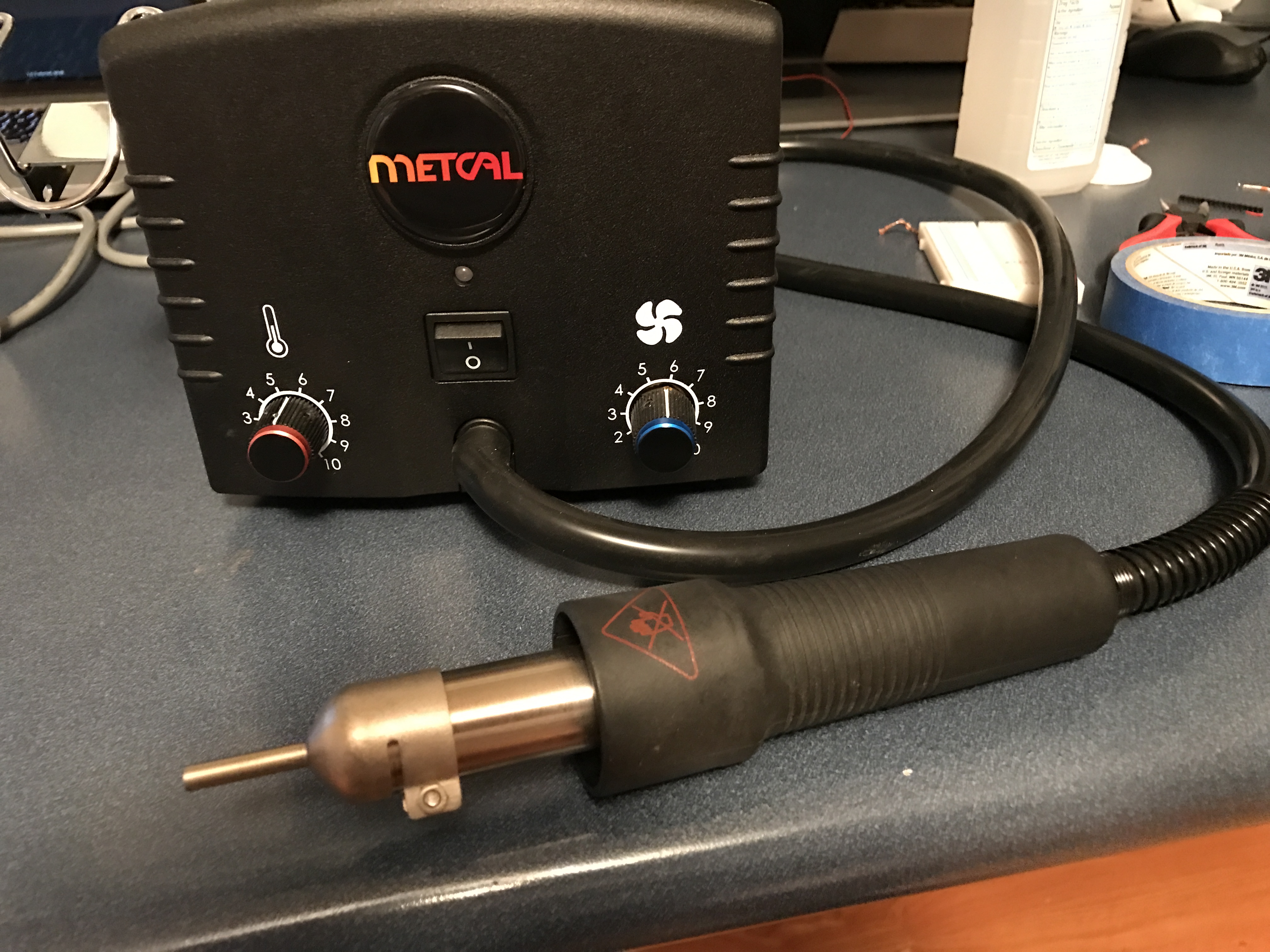
I have a Metcal HCT-900-11 Hand Held Convection Rework tool aka Hot Air Solder tool.  This machine can blow out hot air … really, really hot air, up to about 950 degrees Fahrenheit.  I’m pretty sure you could cut your arm off with it.  The tool has a bunch of nozzles of different shapes and sizes.  Using one of these things is an art form because you need to get the temperature right, the airflow right, the distance from the board right or you will find yourself blowing components off the board and making things worse.

Metcal HCT-900 Hot Air Solder Tool

Pinball machine PCB Solder Problem

In the post where I discussed the first test of the Pinball board I told you that the power supply was not working.  It turns out that the cause of the problem was a big blob of solder under the accelerometer.  To fix that problem I had to remove the tiny little 3x3mm QFN accelerometer using the hot air solder tool.  Once I did, there was a big mess of solder under the package which I cleaned up with a braided copper wick and a soldering iron.  I suspect that I put too much solder onto the pads with the metal stencil when I built the board.

Here is what the board looked like after I cleaned it up:
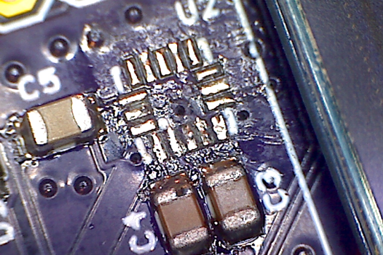
Pinball PCB Solder Problem

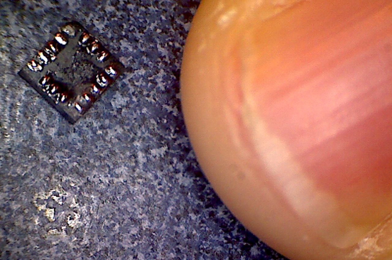
And here is a picture of the damn tiny chip.  The problem with all of these chips is they are meant to be used in cell phones, so they are as small and thin as possible.  And to make matters worse, the pads are on 0.5mm pitch or smaller.

0.5mm QFN with solder problems

Hot Air Solder Rework

When I first started fighting with these QFN problems, I talked to the guys in the Cypress Development Kit team in India.  The manager of the group recorded this video of Jesudasan Moses, who is a wizard with hot air solder tools and a soldering irons.  This video was a huge help and I am grateful to them for recording it.

To fix my problem I followed the same process.  Here is the video:

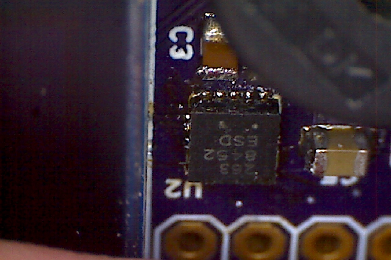
After three attempts, I got the chip  mostly on.  As you can see in the picture below, I was missing a connection to one of the pins.  The other problem was that I melted the screen with the hot air.  Suck.
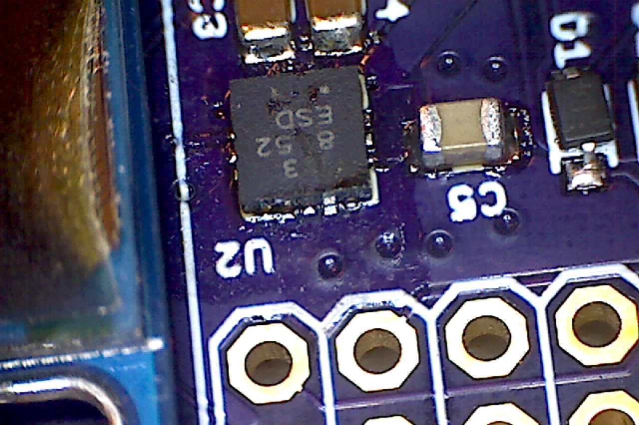
Hot Air Solder rework of 5mm QFN

After I touched up that pin with a soldering iron I still couldn’t talk to it with the PSoC, and I didn’t have easy access to the I2C bus to figure out what was going on.  In the future I need to make sure that there is a place to plug into the I2C bus to debug network traffic.  I will add this to my PCB design guidelines.

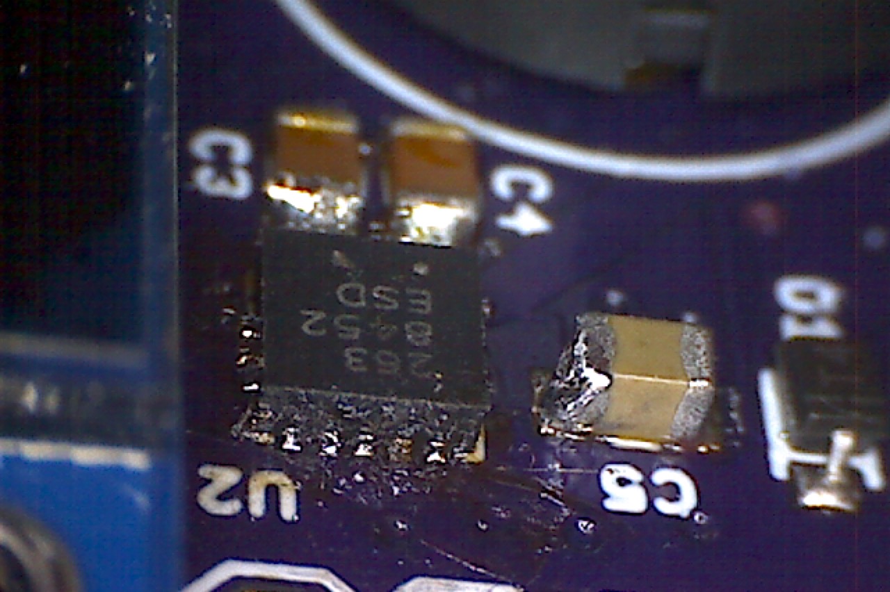
Back to the soldering iron to fix it.  I started by putting some flux on the pins of the QFN package.  Then, I draged a very fine tipped iron with a little bit of solder on it across the pins.  After a couple of rounds of this, I got the chip working.  I still need to cleanup the flux, but here is a picture of one side:

Shorts between pins in 0.5mm QFN

And here is a picture of the other side.  You can see that I mangled the capacitor to the right during the rework process.

Hot Air Solder Repaired QFN

I think that a significant source of problems was not having the entire underside of the QFN with Solder Mask.  That would have helped repel the solder and kept the blob from forming.  I think that I will add that to the checklist as well.

Unfortunately when I was looking at the layout trying to figure out what was going on, I realized that the accelerometer interrupt pin was not connected to the PSoC.  This happened because I had the pins connected by “name” in the schematic.  This is something else that I will add to the checklist.

Using a hot air solder tool is definitely an art form.  One that I will need to practice quite a bit before I get to anywhere near Jesusdan level of skill.

You can find all of the source code and files at the IOTEXPERT site on github.

Index Description
Pinball: Newton's Attic Pinball An introduction to the project and the goals
Pinball: Lotsa Blinking LEDs Everyone needs a bunch of LEDs on their Pinball Machine
Pinball: Matrix LEDs (Part 1) Saving PSoC pins by using a matrix scheme
Pinball: Matrix LEDs (Part 2) Solving some problems with the matrix
Pinball: Matrix LEDs Component How to turn the Matrix LED into a component
Pinball: A Switch Matrix Implementing a bunch of switches
Pinball: Switch Matrix Component (Part 1) The switch matrix component implementation
Pinball: Switch Matrix Component (Part 2) The firmware for matrix component
Pinball: Switch Matrix Component (Part 3) Test firmware for the matrix component
Pinball: The Music Player (Part 1) The schematic and symbol for a Music Player component
Pinball: The Music Player (Part 2) The Public API for the Music Player component
Pinball: The Music Player (Part 3) The firmware to make the sweet sweet music
Pinball: The Music Player (Part 4) The test program for the music player
Pinball: The Motors + HBridge Using an Bridge to control DC Motors
Pinball: The Eagle Schematic All of the circuits into an Eagle schematic
Pinball: The Printed Circuit Board 1.0 The first Eagle PCB layout of the printed circuit board
Pinball: The PCB Version 1.0 Fail Problems with the first version of the Eagle PCB layout
Pinball: PCB Layout 1.2 Updates using Eagle Fixing the errors on the first two versions of the Eagle PCB
Pinball: Assemble and Reflow the 1.2 PCB Assembling the Eagle PCB
Pinball: Testing the Eagle PCB Firmware to test the newly built Pinball printed circuit board
Pinball: Debugging the Motor Driver Fixing the motor driver PSoC project
Pinball: Hot-Air Reworking the Accelerometer Solder Using a Hot-Air Rework tool to reflow a QFN
Pinball: Debugging the LM317 Power Supply- A Tale of Getting Lucky Debugging the LM317/LM117 power supply
Pinball: Debugging the PSoC Motor Driver

Summary

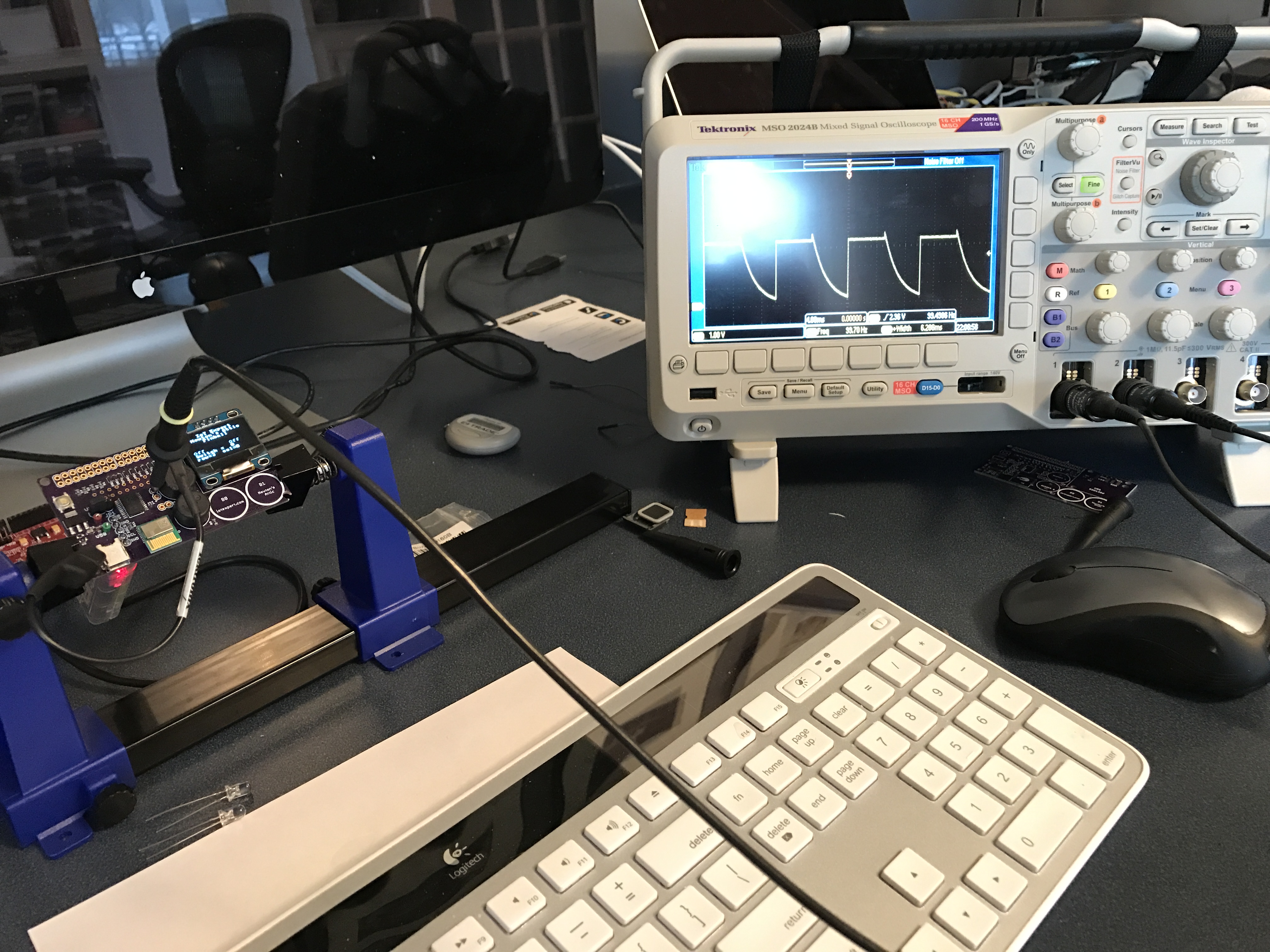
I spent a lot of time the last few days building and testing the Pinball board.  This morning when I plugged in my oscilloscope to test the PSoC motor driver, I saw this:

Pinball Machine PSoC Motor Driver Bug

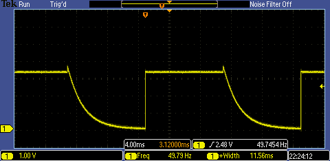
Here is a screenshot directly from the oscilloscope.  When I saw this, I wondered what was going on.  Why does the driver pull-up very quickly, but have some kind of RC delay on the pull-down?  This was particularly troubling as the PWM was set to 50 Hz (see on the picture where the (1) Freq is showing the measurement)

Broken Motor Driver Output

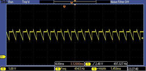
Things got much worse when I increased the frequency to 500 Hz.  In fact, the motor driver doesn’t pull-down at all.

Crazy PWM Output

PSoC Motor Driver

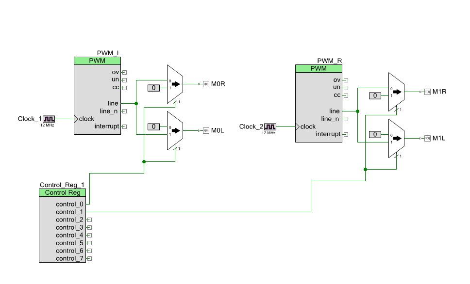
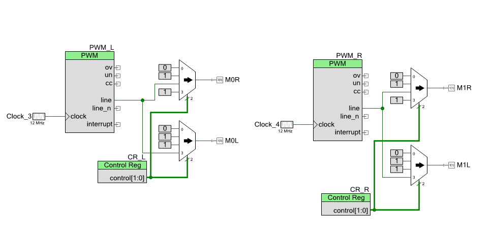
So where do I start debugging?  First I looked at the PSoC Creator schematic.  When you look at the schematic you can see that I took the PWM output and steered it to either M0L or M0R (or M1L or M1R).  Then I used a control register to flip it.

PSoC Motor Driver Schematic (broken)

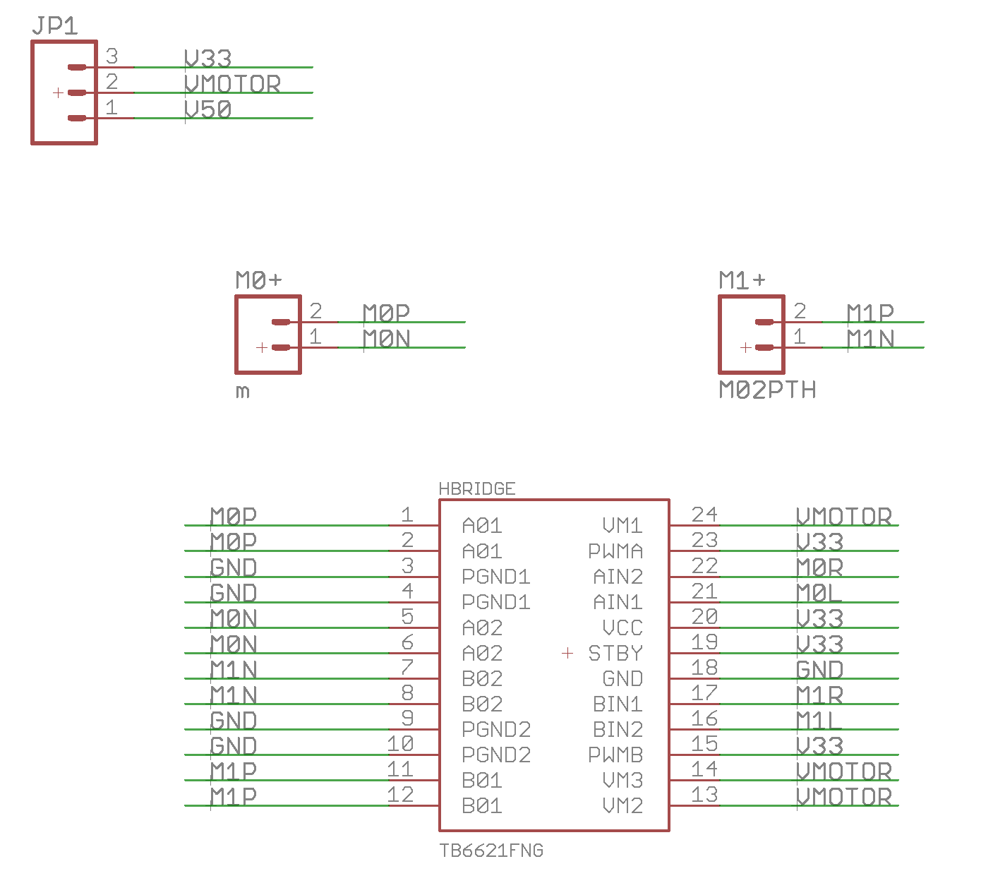
The M0R/M0L signals are used to control the switches on the H-Bridge.  Here is the actual schematic from the PCB:

PSoC Motor Driver Schematic

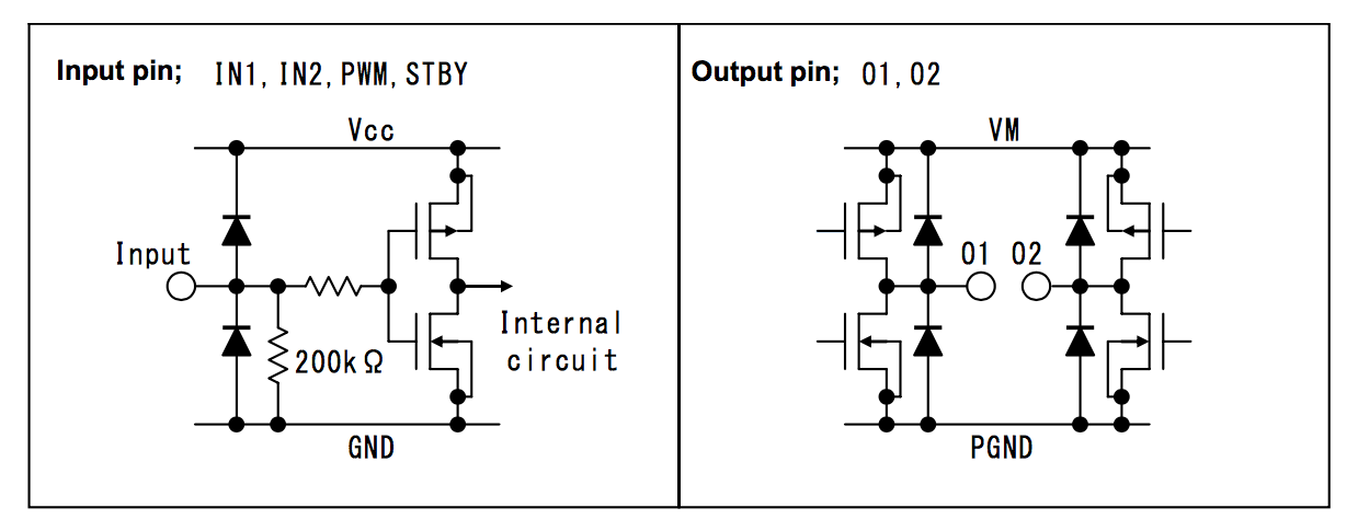
I chose the Toshiba TB6612FNG motor driver chip for this design.  It has two H-Bridges built in and is the same one that we used on the PSoC 211 Robot.  You can see from the schematics above that I save 1 pin by attaching the PWM input to “H(igh)” and that I pulse either In1 or In2.

Hbridge Schematic

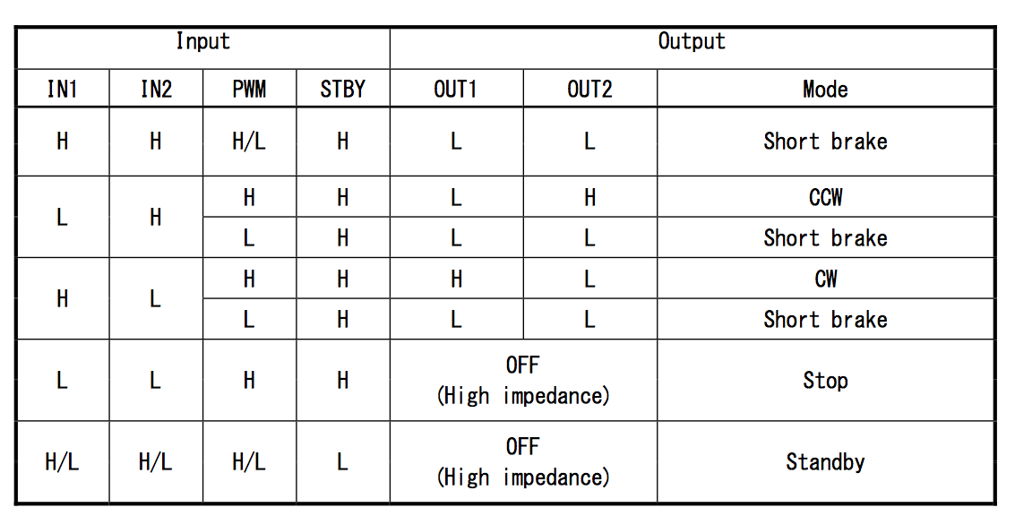
When you look at this table, or the schematic, you’ll see my problem.  I connected one of the inputs to “L”  That means that the NMOS switch that controls the pull-down is always off.  When the PWM is low, there is no pull-down.  That explains the funny RC pull-down, which is just some leakage on that node.

HBridge Truth Table


To fix this, I make this change to my PSoC Creator schematic.  In this configuration I get the following:

CR=00 the output = 00 (stop)

CR=02 the output = 1PWM = CCW

CR=03 the output = PWM1 = CW

PSoC Motor Driver Schematic

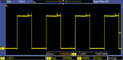
Now when I run this thing, here is what I get (at my desired 20KHz):

Oscilloscope of functioning PSoC Motor Driver

And finally a video showing the PSoC Motor Driver working:

ThingSoC: Four I2C OLED Displays with PSoC4L

Pattern Agents are running a crowd funding effort for ThingSoC TSoC4L … help them here

Summary

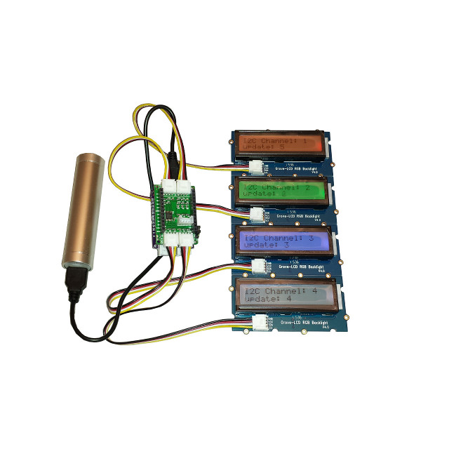
In the previous ThingSoC post I took you through building the firmware to make the PSoC4L drive the ThingSoC I2C hub.  Now what?  When originally looking around I saw a picture with 4x LCDs connected to the I2C hub, which I thought was cool. In this post Ill show you how to do the same thing with PSoC and the U8G2 library which I talked about in this article. To do this I will:

  1. Create New PSoC4L Project + Integrate the U8G2 Library
  2. Update the PSoC4L Firmware
  3. Test the PSoC4L Firmware

Here is the picture:

4 I2C Displays, Inspiration

Create New PSOC4L Project + Integrate the U8G2 Library

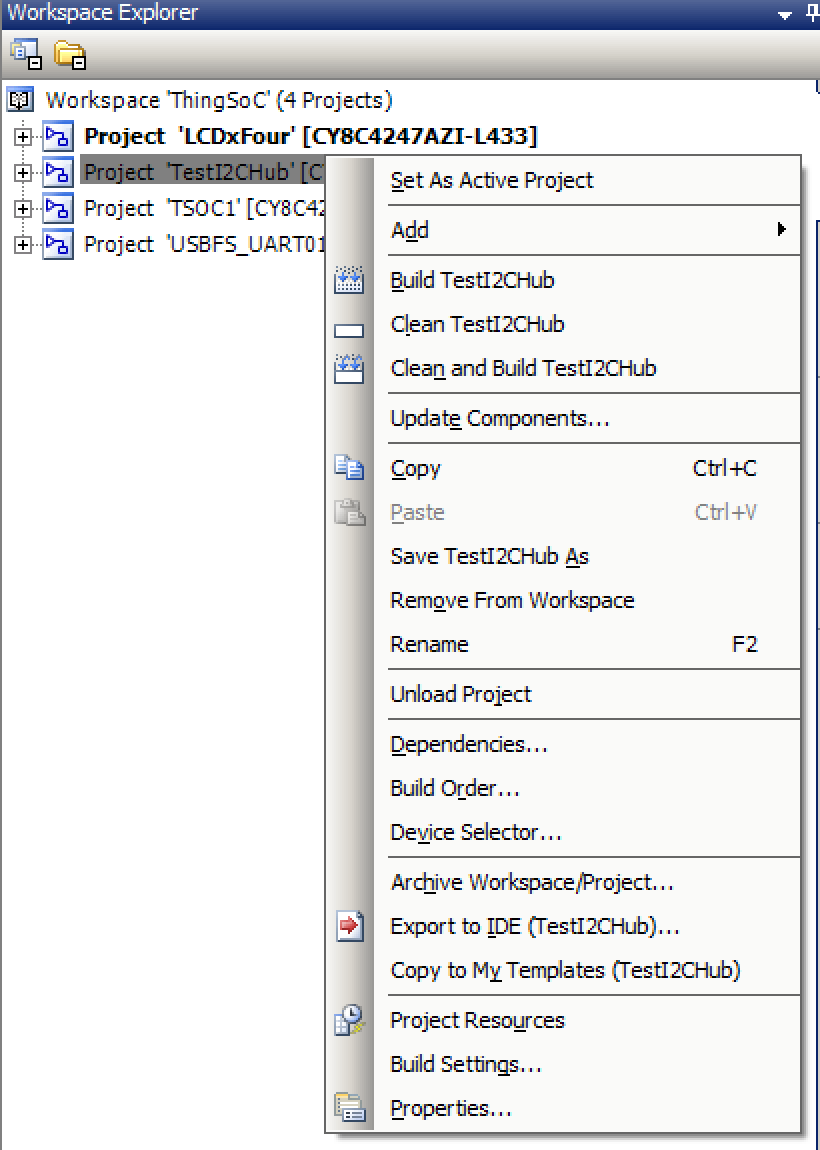
Maybe it should have been obvious, but for some reason it never occurred to me to do a copy/paste to duplicate a project.  I guess that I’m slow that way.  To do this right click on a project in the workspace explorer and then do paste.

PSoC Creator Edit Build Settings

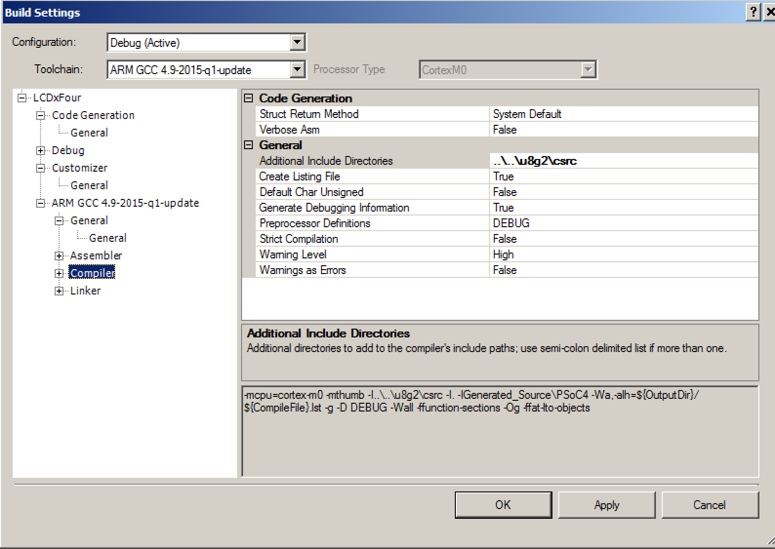
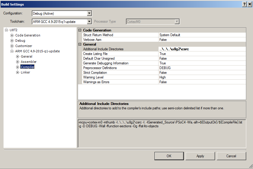
The next step is to integrate the firmware from the U8G2 Library. Start by “gitting” with “git@github.com:olikraus/u8g2.git”.  Then you need to add the directory to your project by right clicking the project and selecting “Build Settings”.  You need to add U8G2 Library to the additional include directories.

Add the U8G2 Library

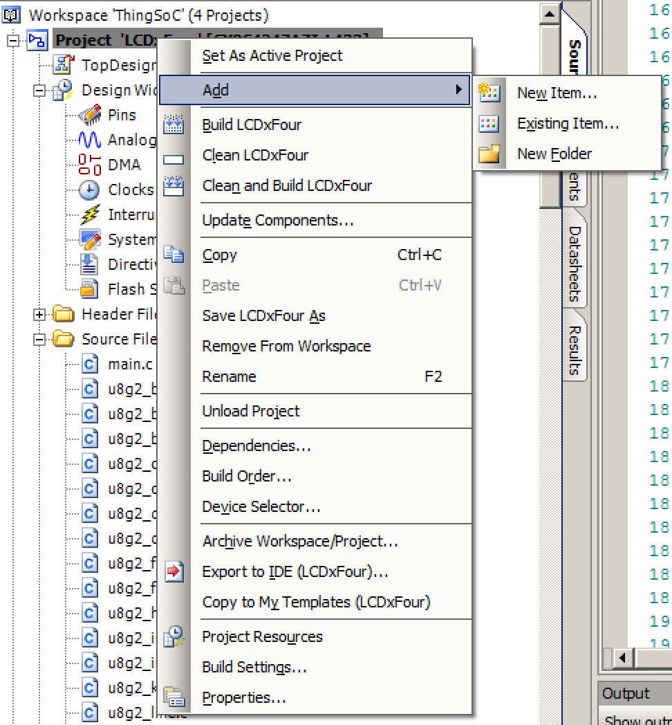
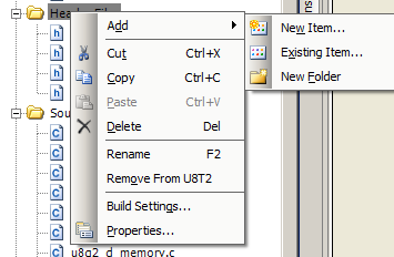
Add the all of the .h and .c files by right clicking the project and selection “Add->Existing Item”

copy the u8g2 files into the PSoC4L project

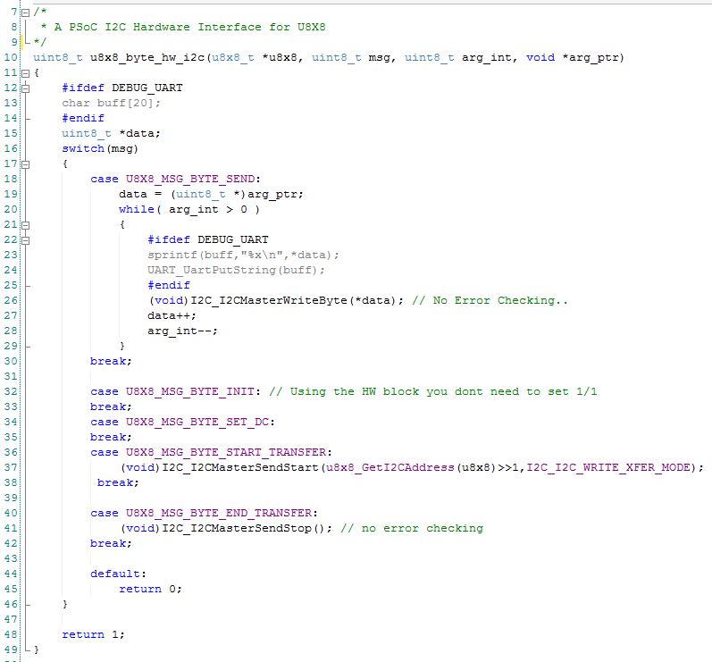
Navigate to the U8G2 library and add all of the .c and .h files.  The last thing you need is to bring in the HAL that I wrote for PSoC and described in this post.  Specifically you need to bring in the two functions

  • psoc_gpio_and_delay_cb
  • u8x8_byte_hw_i2c

I suppose that I should package the whole thing up in a component.  But, Ill leave that as an exercise for the reader.

Update the PSoC4L Firmware

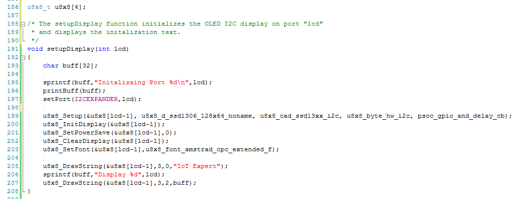
The cool thing about the whole setup with the I2CHUB is that it allows you to have 4 devices with the same I2C address attached to one PSoC SCB at the same time.  To get going with the firmware, I start by defining an array of u8x8_t structures to represent the 4 different displays attaches to the 4 different ports on the I2C hub. (line 186).  Then I create a function called setupDisplay that initializes the display etc. (lines 199-203).  The only trick in the firmware is that Dennis Ritchie defined arrays to run from 0-3 but the I2C busses are labeled 1-4,  this is the reason for subtracting 1 from the input lcd number.

PSoC4L Firmware to initialize the U8G2 Display

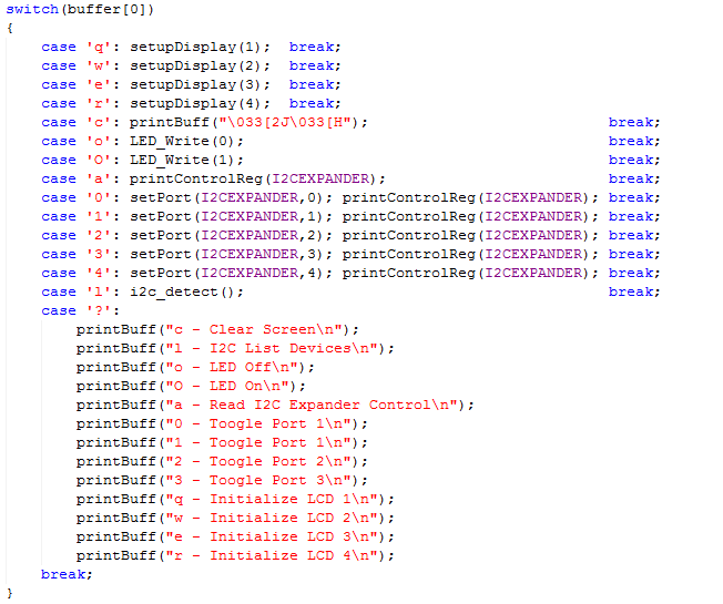
The next step is modifying command processors in the main loop.  Specifically, I will add the commands q,w,e,r to startup the displays on I2C ports 1,2,3,4.  And, I will add those commands to the help print out.

Modifying the PSoC4L CLI

Test the PSoC4L Firmware

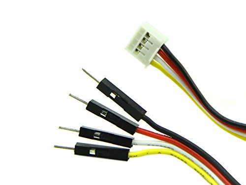
In order to make a connection from the Grove 4-pin connectors to my breadboard I used Switch Doc Labs connectors which I bought from Amazon.com.  For some reason you can’t purchase them from the Switch Doc Labs website or the SeeedStudio website, but they are very handy.  As an unrelated side note I had never seen (or in fact ever heard of) Switch Doc Labs.  But their website has a bunch of tutorials about the Raspberry Pi and Grove ecosystem boards for use with IoT-ifying house plants.  Seemed pretty cool.

Grove to Breadboard Switch Doc Labs Breakout Cable

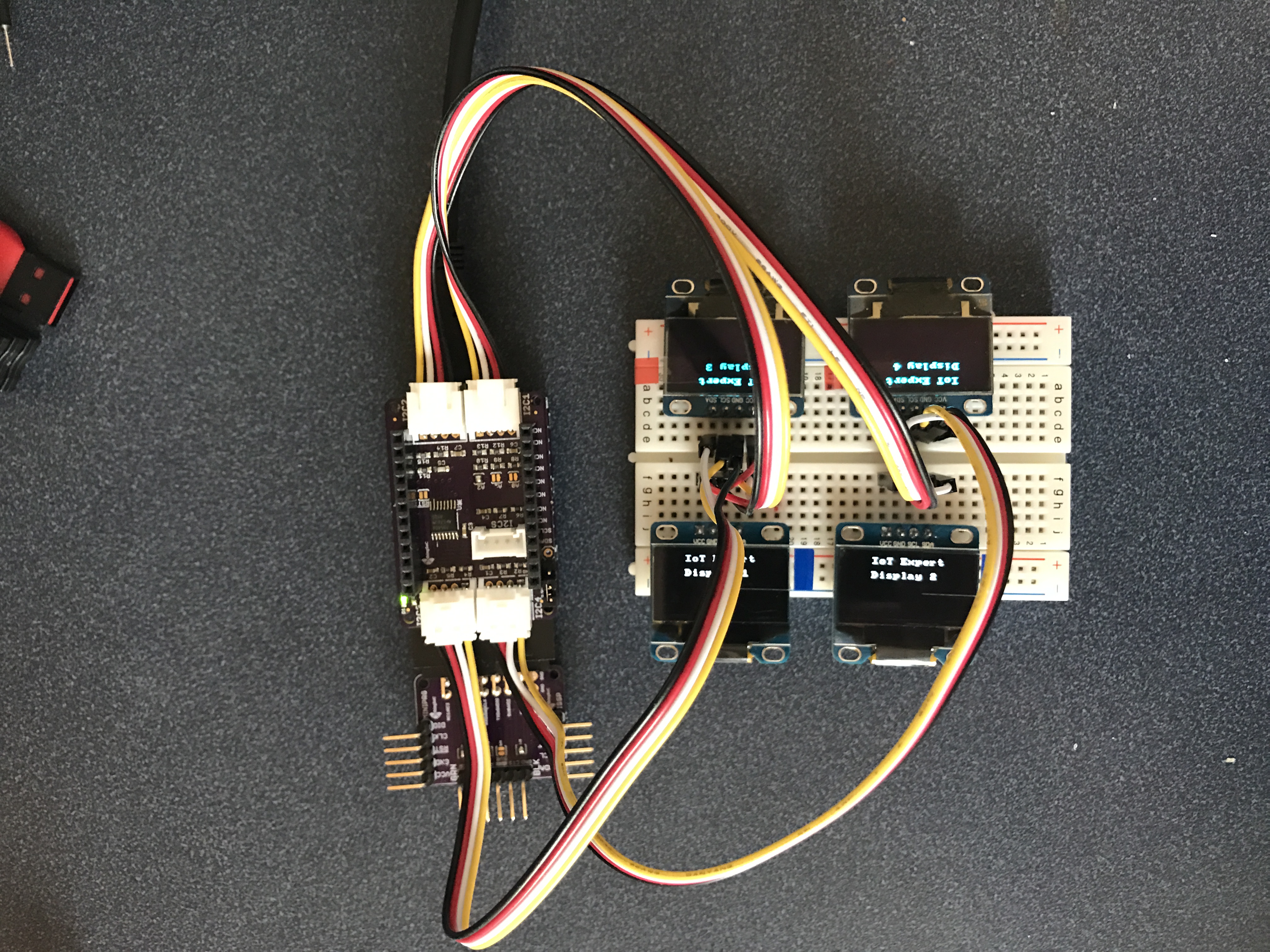
Now when I press “qwer” in my command console I get this:

PSoC4L Driving 4 OLED LCDs

You can find all of the projects in the TSoC Series at my GitHub ThingSoC repository git@github.com:iotexpert/ThingSoC.git

Index Description
ThingSoc: TSoC PSoC4L Development Kit from PatternAgents Introduction to ThingSoC
ThingSoC PSoC4L: Using & Debugging the PSoC4 Clock Debugging a beta firmware problem
ThingSoC: The TSoC GROVEY I2CHUB : I2C Hub/Switch Evaluating the ThingSoC I2C Hub
ThingSoC: Multiple I2C Displays Using the I2CHUB and U8X8 Library A project using ThingSoC I2C Hub & 4 OLED Displays

ThingSoC: The TSoC GROVEY I2CHUB : I2C Hub/Switch

Pattern Agents are running a crowd funding effort for ThingSoC TSoC4L … help them here

Summary

One of the boards that the Pattern Agents guys sent me was a TSOC GROVEY I2CHUB : I2C Hub/Switch.  In this post I will take you through the process that I went through to evaluate the board and build an interface to the ThingSoc TSoC 4L base board.

  1. Introduction to the TSoC Grovey I2CHUB
  2. Discussion of PCA9546A I2C
  3. Using the MiniProg-3 to interact with the PCA9546A
  4. Building a Command Line Interface (CLI) using the USB/UART
  5. Adding firmware to mimic the MiniProg-3 I2C list to the CLI
  6. Adding a “port change” feature to the CLI firmware

Introduction to the TSoC Grovey I2CHUB

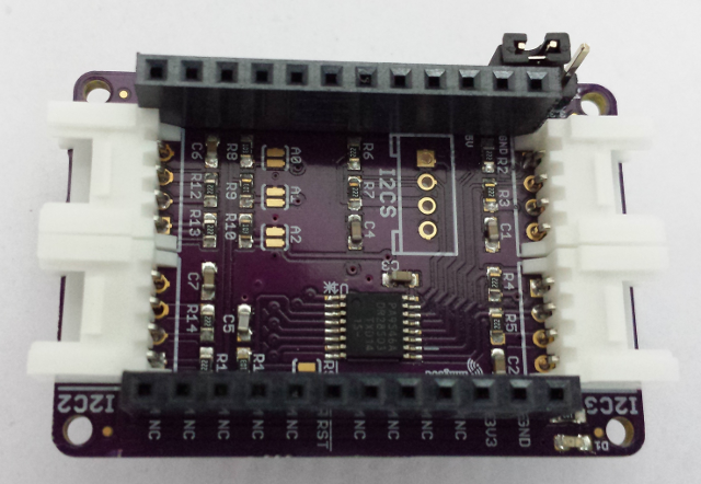
The ThingSoC I2C Hub is a ThingSoC Compatible (not Compliant) board that serves as a bridge from the base board to 4 separate programmable I2C busses using an NXP/TI 9546A bridge chip.  Each of the I2C busses is attached via a SeeedStudio Grove connector.  Grove is an ecosystem of sensors (Humidity, Temperature etc.) that are all? mostly? I2C connected.

ThingSoC I2CHub

Discussion of PCA9546A I2C

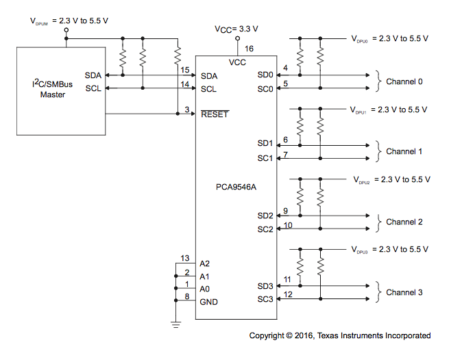
The PCA9546A is made by TI and NXP (or whatever they are calling themselves these days) and can be purchased for about $0.70 from Digikey, Mouser, or Arrow.  The chip is pretty cool.  It will let you connect your I2C master to 1 of 4 I2C busses.  It will actually let you connect more than one bus at a time.  This chip enables you to connect multiple slaves with the same address to your I2C master.

Here is a simplified picture from TIs datasheet.

PCA9546A Block Diagram

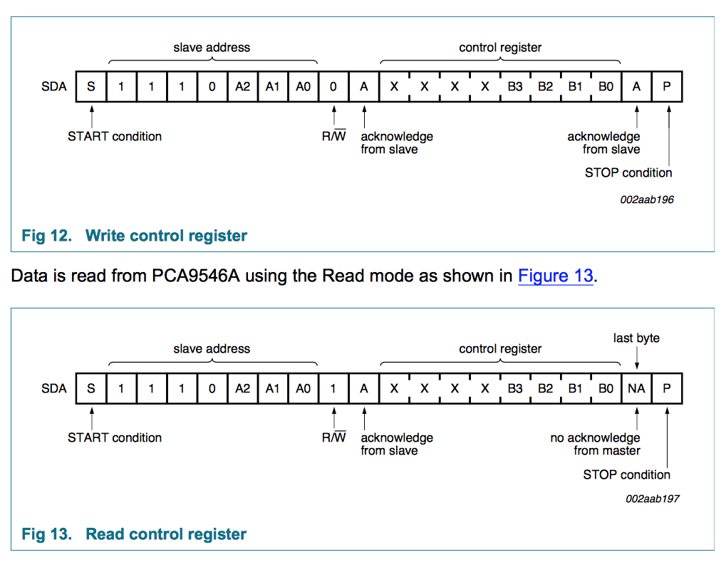
To control the system you just need to write into the control register with a bit mask.  The bit masks contains which slaves busses you want switched on.  Here is a screen shot from NXPs datasheet:

PCA9546A Control Register

Using the MiniProg-3 to interact with the PCA9546A

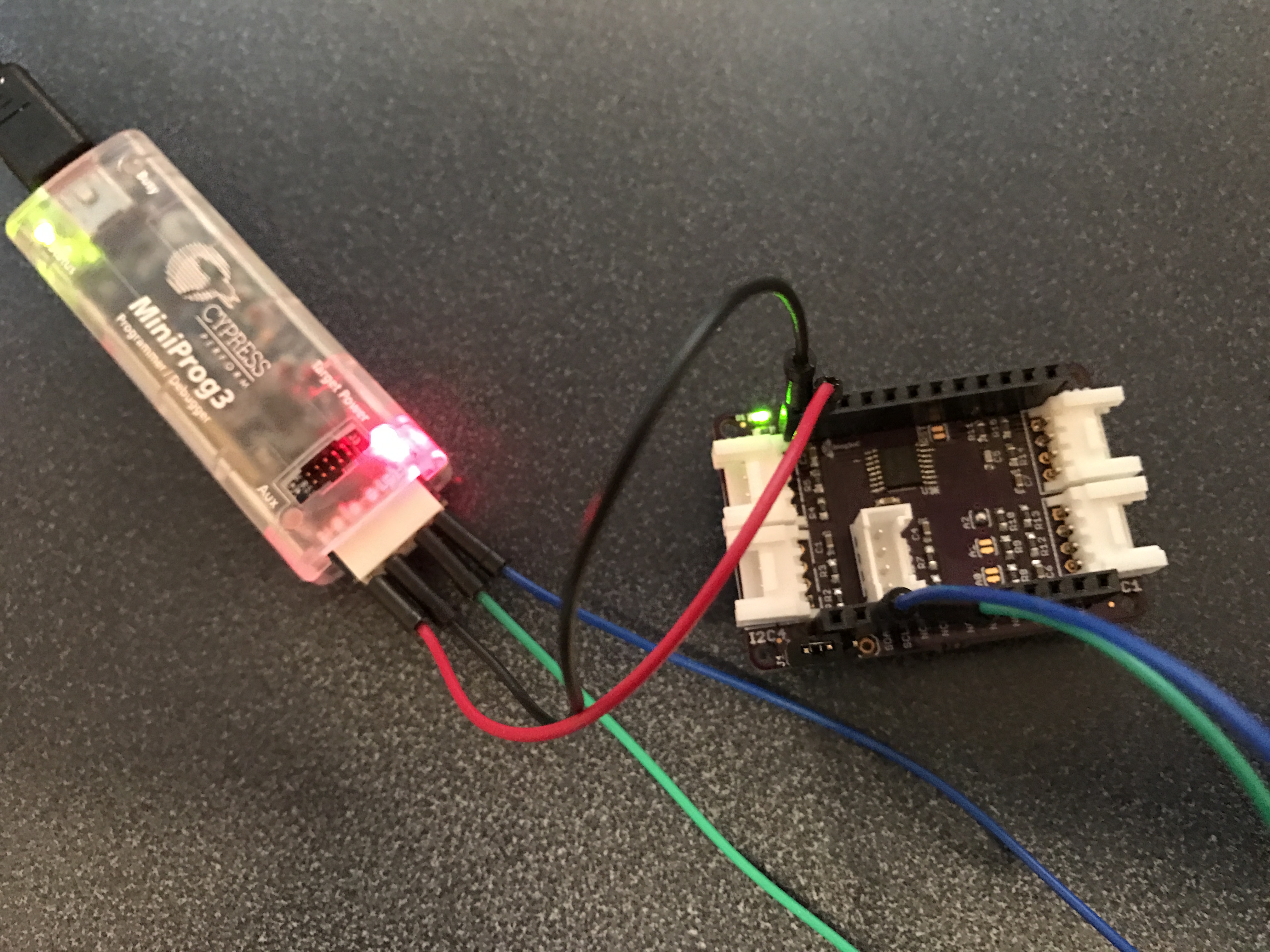
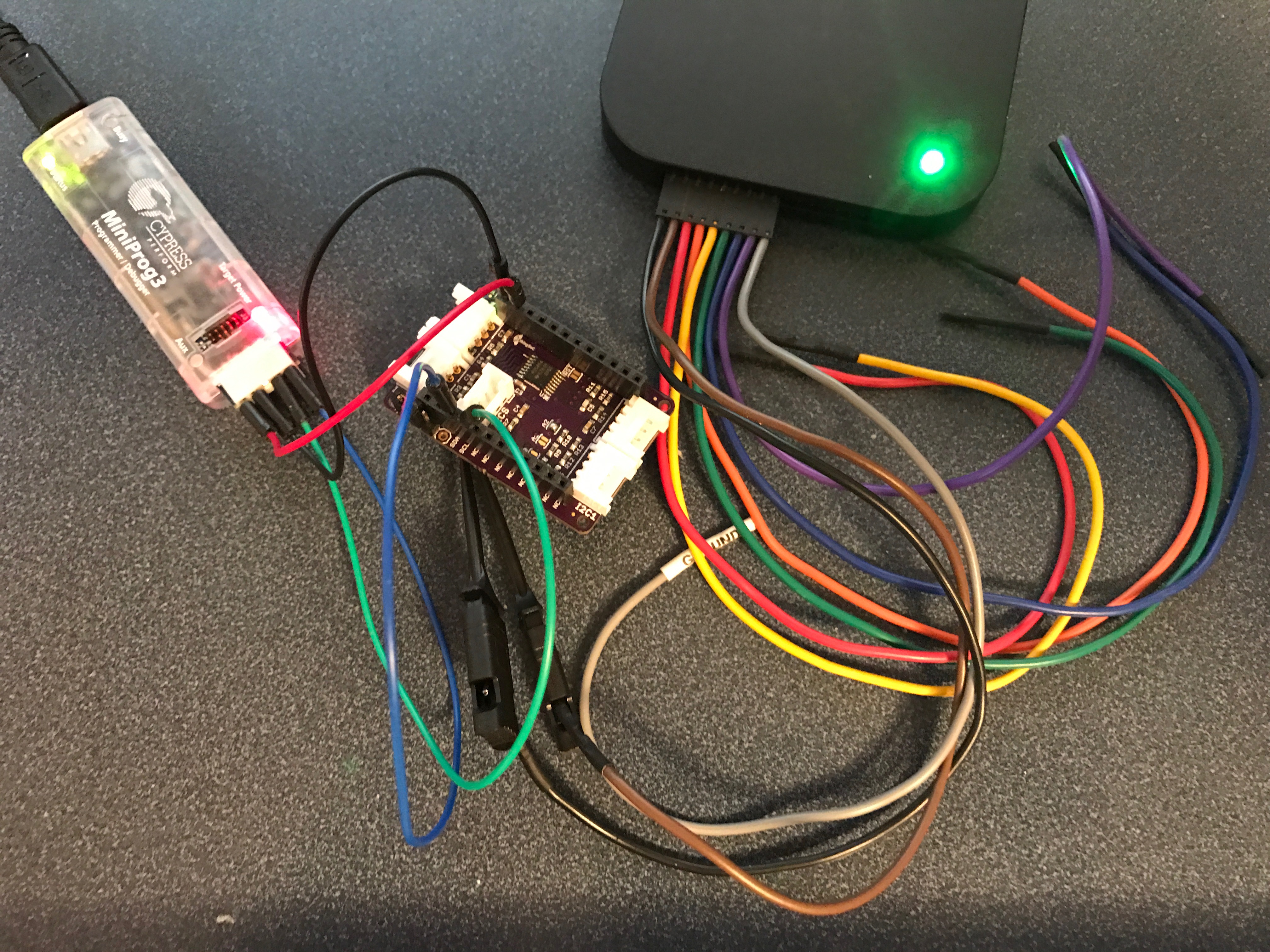
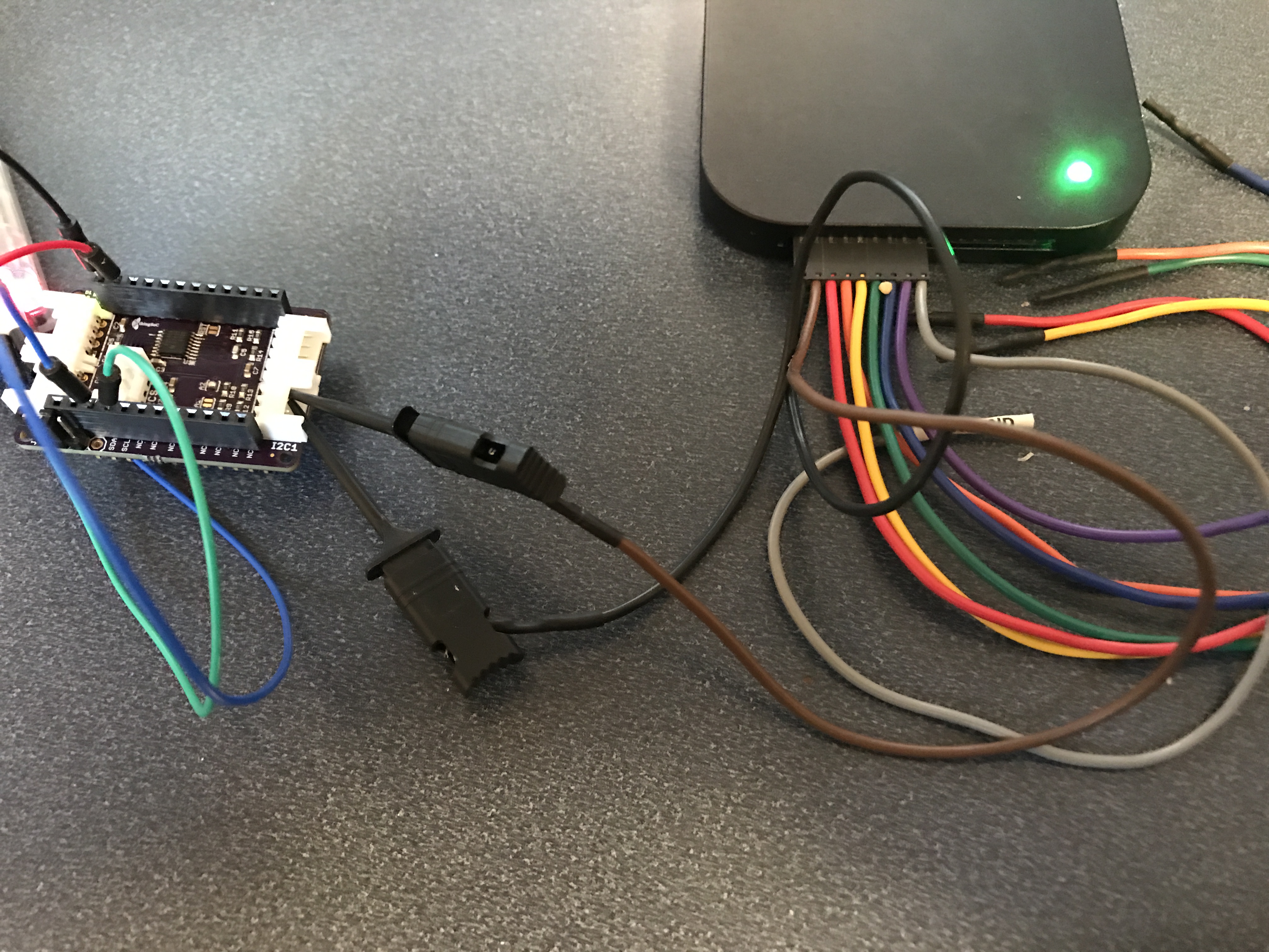
I start the whole firmware journey by using a MiniProg-3 as an I2C<–>USB bridge.  This allows me to type I2C commands in the Bridge Control Panel which go directly to the chip (without writing firmware).  In the picture below you can see that I have the MiniProg-3 attached to the ThingSoC board using jumper wires.  I also use the MiniProg-3 to power the board.

Using a MiniProg-3 to Probe the ThingSoC I2C Hub

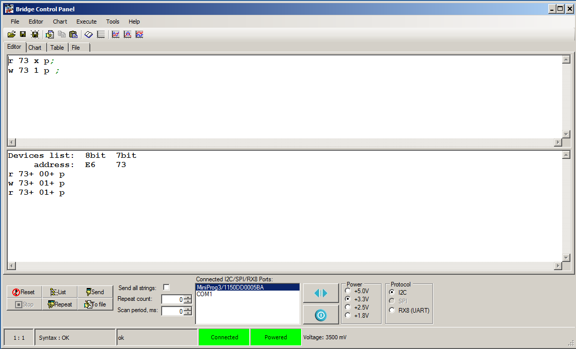
When I press “List”, the Bridge Control Panel probes all of the I2C addresses.  If a device ACKs, it prints out that fact in the output window.  In the picture below you can see that PCA9546A is attached at address 0x73.  I then read and write the control register, which also works as expected.

Bridge Control Panel

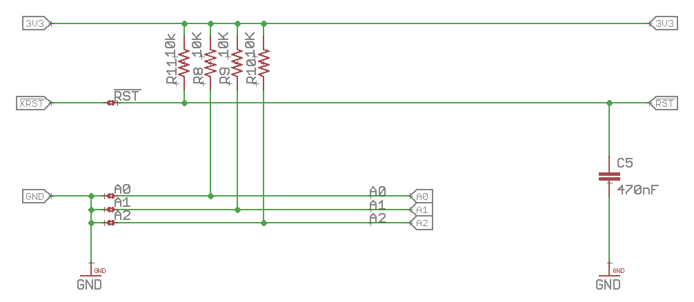
The address 0x73 makes sense as you can see that (in the picture above) there is a blob of solder on “A2” which pulls it low (instead of the default high).  Here is that part of the schematic:

ThingSoC Schematic for PCA9546A Address Selection

Building a Command Line Interface (CLI) over the USB/UART

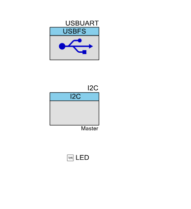
Now I am  ready to build a command line interface using the USB <–> UART Bridge.  First, I make a schematic with the USB-FS (Full Speed), LED and I2C components.  Notice that the USBFS is setup as a USBUART.  The I2C is configured as a Master.

PSoC Creator Schematic for ThingSoC I2C Hub Firmware

The Pins are selected as:

PSoC Creator Pin Selection

Next is a helper function to printout text via the CDC UART:

PSoC Creator Firmware PrintBuff Helper Function

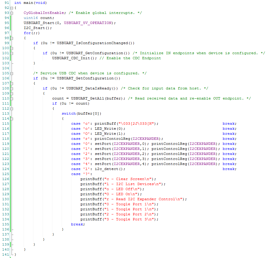
Then I write a little bit of firmware for the CLI.  The function just reads from the UART and, if the user has pressed a button, then it issues that command.

Lines 99-103 get the USBUART going, and deal with changes (e.g. unplug events).

The only thing that you might not have seen is the “Clear Screen”.  I just send out the escape sequence (old school) for clear screen and move home from the VT100 Escape Codes.

PSoC Creator Main Command Line Interface

Adding firmware to mimic the MiniProg-3 I2C list to the CLI

When you press “List” in the Bridge Control Panel, what happens?  Although I have been using the Bridge Control Panel for years I wasn’t exactly sure.  To find the answer, I plugged in my Saleae Logic 16 and watched the output.

Probing using MiniProg-3 and Saleae Logic-16

In this screenshot from the Saleae Logic output screen,  you can see that the Bridge Control Panel sends out a “Read 0x15” which was NAKed.

Saleae Logic 16 address 0x15 NAK

In this screen shot you can see that when the “Read 0x73” occurs, that the PCA9456A ACKs which tells the Bridge Control Panel that the device is there.

Saleae Logic 16 0x73 ACK

While I was writing the entry, I looked around at several implementations.  It appears that sometimes people send “Write Address” instead of “Read Address”.  I wasn’t sure exactly what was right, so I consulted Dr. Zwave.  He really should go by Dr. I2C since that is what he did at Cypress.  Anyway, he pointed out that you will hang the I2C bus if you try a Read and then don’t read the next byte.  With a write you don’t actually need to keep writing.  I decided to follow his instructions.

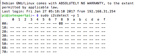
I have always liked the output of the Raspberry Pi I2CDetect command.  Here is a screen shot from one of my Raspberry Pi’s where a PSoC4 is attached on I2C Address 0x8.  I am not totally sure why the command does not probe addresses 0x00-0x02 (comment with the answer and Ill send you a devkit)

Raspberry Pi I2CDetect

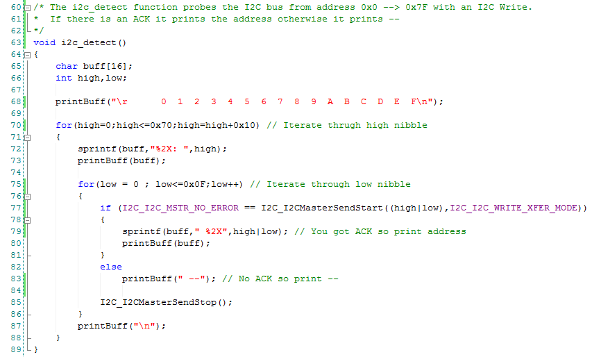
The implementation of i2c_detect on the PSoC4L is pretty simple.  All I need to do is iterate through all of the addresses from 0->0x7F.  Then attempt to write.  If a device ACKs then printout the address, otherwise move on.  Instead of  one big loop, I split it up into two loops to make the printing a little bit simpler.  Here is the code:

PSoC Creator I2C Detect Firmware

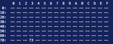
Now, when I press “l” on the CLI, it probes all of the legal addresses on the I2C bus from the PSoC4L.  You can see that only the PCA9546A at address 0x73 is active.  How cool is that?

PSoC Creator Firmware I2CDetect

Adding a “port change” feature to the CLI firmware

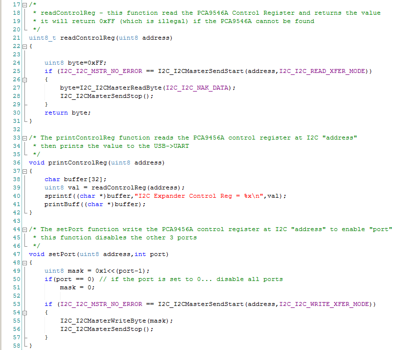
The last block of code adds three functions which let me control the PCA9546A control register.

PSoC Creator PCA9546A Control Firmware

To test the whole thing, I attach the Saleae Logic Analzer to I2C Port1.  Then I probe to make sure that I can attach and unattached the bus.

Test Jig for PSoC Creator Firmware

You can find all of the projects in the TSoC Series at my GitHub ThingSoC repository git@github.com:iotexpert/ThingSoC.git

Index Description
ThingSoc: TSoC PSoC4L Development Kit from PatternAgents Introduction to ThingSoC
ThingSoC PSoC4L: Using & Debugging the PSoC4 Clock Debugging a beta firmware problem
ThingSoC: The TSoC GROVEY I2CHUB : I2C Hub/Switch Evaluating the ThingSoC I2C Hub
ThingSoC: Multiple I2C Displays Using the I2CHUB and U8X8 Library A project using ThingSoC I2C Hub & 4 OLED Displays

Pinball: Driving the OLED using the U8G2 Library

In the previous Pinball post, I wrote about getting the OLED going and getting the footprint onto my printed circuit board.  Now I need to make PSoC firmware to drive the display.  I turns out that there are a number of different driver chips out there including at least SSD1306, SH1106, LD7032, SSD1325, and ST7920 that handle multiplexing the columns/rows, managing frame buffers, power management, etc.  To make matters more fun, these chips support I2C, 3&4 wire SPI and a couple of different parallel interfaces (6800, 8080).  I certainly didn’t want to go down the rathole of building up a complete driver library.  But I didn’t have to, as it turns out that that Oliver Kraus built and open-sourced a very nice library that you can get at www.github.com/olikraus/u8g2.  This library (and its predecessor u8glib) seem to be in pretty wide use in Arduino and Raspberry Pi.

In order to make the library work with the PSoC I had to do several things

  1. Download it from GitHub (git clone git@github.com:olikraus/u8g2.git)
  2. Created a new PSoC4200M project for the CY8CKIT-044 (which was the devkit that I happened to have sitting next to my computer)
  3. Change the build settings (right click on the project and select building settings) then add the directory in “Additional Include Directories” and include the “u8g2/csrc” directory.
  4. Add the header files to the project by right clicking and selecting “Add->Existing item” so that the project can f
  5. Add the U8G2 C-Files to the project (same as step 4 but add the C files)
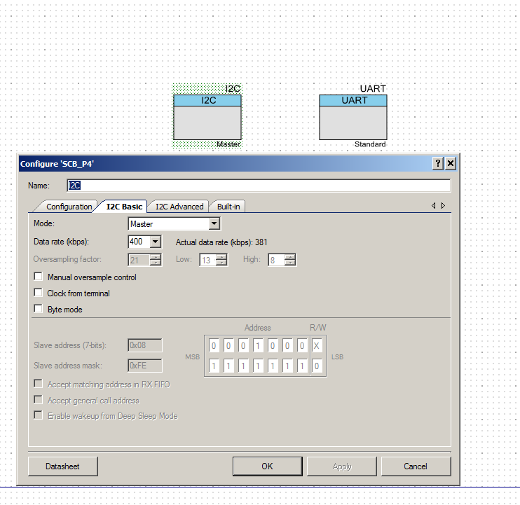
  6. Build a schematic which has an I2C (for the display) and a debugging UART.  The I2C is configured as a master with 400kbs data rate.  The UART uses the default configuration.
  7. Assign the pins

Now I am ready to build some firmware that will drive the display.  In order to use the library with a PSoC I need to create two functions for the U8G2 HAL to use as an interface to the PSoC hardware.  You initialize the U8G2 system with a call to the u8x8_Setup function.  In that call you need to provide function pointers too the two HAL functions

  1. The GPIO and Delay Interface
  2. The byte oriented communication interface

This is an example of the setup required:

The GPIO and Delay interface is used by the byte oriented communication functions to read/write the GPIOs and provide delays.  This function provides the underpinnings of a bit-banged I2C, UART, SPI etc.  Because I am only going to use PSoC Hardware to provide the I2C interface I will only respond to the delay messages.  All of the delay functions are implemented as busy wait loops, which I am not a big fan of.  The input to the function is a “message” that is one of a sprawling list of #defines in the file u8x8.h.  I believe that I found all of the possible cases, but I am not sure.

The first message, UX8X8_MSG_GPIO_AND_DELAY_INIT doesnt need to do anything because the GPIOs are configured correctly by the default.

I did not respond to the messages of the form U8X8_MSG_GPIO_X which are the read and write of the GPIOs as I am not going to use the bit-banged interface.

The other function that needs to be provided is the byte-oriented communication function.  This function needs to respond to the messages to start, send, and end communication.  I just mapped those messages onto the PSoC hardware APIs.  While I was trying to understand what was happening with the system I implemented a debugging UART which you can see in the #ifdef DEBUG_UART sections.

You can find all of the source code and files at the IOTEXPERT site on github.

Index Description
Pinball: Newton's Attic Pinball An introduction to the project and the goals
Pinball: Lotsa Blinking LEDs Everyone needs a bunch of LEDs on their Pinball Machine
Pinball: Matrix LEDs (Part 1) Saving PSoC pins by using a matrix scheme
Pinball: Matrix LEDs (Part 2) Solving some problems with the matrix
Pinball: Matrix LEDs Component How to turn the Matrix LED into a component
Pinball: A Switch Matrix Implementing a bunch of switches
Pinball: Switch Matrix Component (Part 1) The switch matrix component implementation
Pinball: Switch Matrix Component (Part 2) The firmware for matrix component
Pinball: Switch Matrix Component (Part 3) Test firmware for the matrix component
Pinball: The Music Player (Part 1) The schematic and symbol for a Music Player component
Pinball: The Music Player (Part 2) The Public API for the Music Player component
Pinball: The Music Player (Part 3) The firmware to make the sweet sweet music
Pinball: The Music Player (Part 4) The test program for the music player
Pinball: The Motors + HBridge Using an Bridge to control DC Motors
Pinball: The Eagle Schematic All of the circuits into an Eagle schematic
Pinball: The Printed Circuit Board 1.0 The first Eagle PCB layout of the printed circuit board
Pinball: The PCB Version 1.0 Fail Problems with the first version of the Eagle PCB layout
Pinball: PCB Layout 1.2 Updates using Eagle Fixing the errors on the first two versions of the Eagle PCB
Pinball: Assemble and Reflow the 1.2 PCB Assembling the Eagle PCB
Pinball: Testing the Eagle PCB Firmware to test the newly built Pinball printed circuit board
Pinball: Debugging the Motor Driver Fixing the motor driver PSoC project
Pinball: Hot-Air Reworking the Accelerometer Solder Using a Hot-Air Rework tool to reflow a QFN
Pinball: Debugging the LM317 Power Supply- A Tale of Getting Lucky Debugging the LM317/LM117 power supply
ThingSoC PSoC4L: Using & Debugging the PSoC4 Clock

Pattern Agents are running a crowd funding effort for TSoC … here

Summary

In the previous post I told you that I immediately blew away the factory firmware on the TSoC4L board.  I’m like that sometimes :-).  In this post I am going to take you through the entire process of getting and reprogramming the factory firmware, then finding and debugging a PSoC4 clock problem.  The rest of this post is:

  1. Getting the correct firmware back on the TSoC4L Board
  2. Running into a bug in the beta version of the firmware
  3. Using the debugger to find the bug
  4. Explaining the functionality of Low Frequency Clocks and the Watch Dog Timer
  5. The Pattern Agents bug fix

Factory Firmware

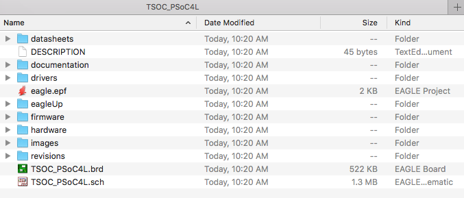
Getting things going again starts with “git”ing the firmware.  This can be done by “git clone git@github.com:PatternAgents/TSOC_PSoC4L.git”.  Once you have the repo cloned you will find a bunch of good stuff including:

  1. datasheets: All the datasheets
  2. documentation: The PatternAgents documentation (quick start)
  3. drivers: The windows USB <-> UART drivers
  4. eagleUp: JPG renderings of the PCB
  5. firmware: The PSoC Creator Project
  6. hardware: gerbers, boms etc
  7. images: renderings of the board, photos of the board etc
  8. revisions: old revisions of the Eagle project files
  9. The Eagle PCB Project including schematic and layout

TSoC4 L Files from GitHub

When you open the PSoC Creator Workspace you will find two projects

  1. A USB Bootloader – called “USBFS_Bootloader”
  2. The TSoC RSVP Firmware – called “rspvsis_4l_typ”

The system is supposed to

  1. Start the USB HID bootloader (so you could get new firmware).  Wait for 10 seconds for a bootloader host to start then if it doesnt … then start
  2. The RSVP Firmware

When you plug in the board you will see the TSoC4L enumerate as “Cypress ThingSoc Bootloader”.  Then, after 10 seconds, you should see it reboot, then enumerate as “Cypress USB UART”.  But, this was not happening for me.  Why?  I wasn’t sure.  The first thing that I did was add a blinking LED circuit that looked like this:

Blinking LED

But the LED was not blinking.  That meant that the firmware was not even getting to main i.e. it was hanging BEFORE main in the PSoC boot code.  But where and why?

Using the Debugger to Find the Bug

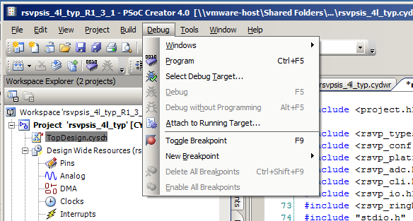
How do you figure out where the system is stuck if you can’t even use the “blinking LED” or “printf” debug?  Simple.  Use the debugger.  Start by programming the PSoC with your firmware.  Then click “Debug->Attach to running target”.

Starting the PSoC Debugger

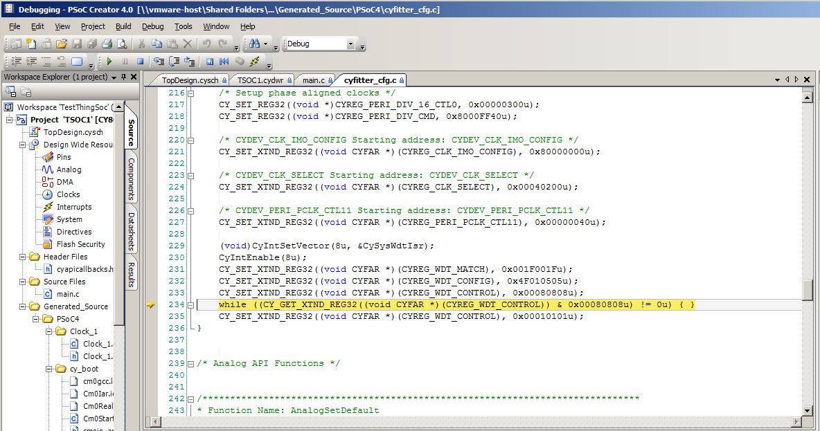
The debugger will start.  Then you will be able to press the “Pause” button. which will take you to a screen that looks like this:

PSoC4 Clock Busy Wait Loop

The chip is stuck on line 234.  What does line 234 do?  That is a busy wait loop.  It is waiting for the Watch Dog Control Register to clear.  To explain that, I will need to take you through the PSoC4 Low Frequency Clocks.  First you should notice that the file we are in is named “cyfitter_cfg.c”.  What is this file?  If you look at the top, this is what PSoC Creator says.

This means that the “cyfitter_cfg.c” file is synthesized by PSoC Creator when you do a build based on what you configured when you setup your project.  This file contains a bunch of the startup code including the code that gets the clock systems going.  Line 234 is inside of a function called “ClockSetup”.  All of this code is called BEFORE you get to main().

The PSoC4 Clock(s)

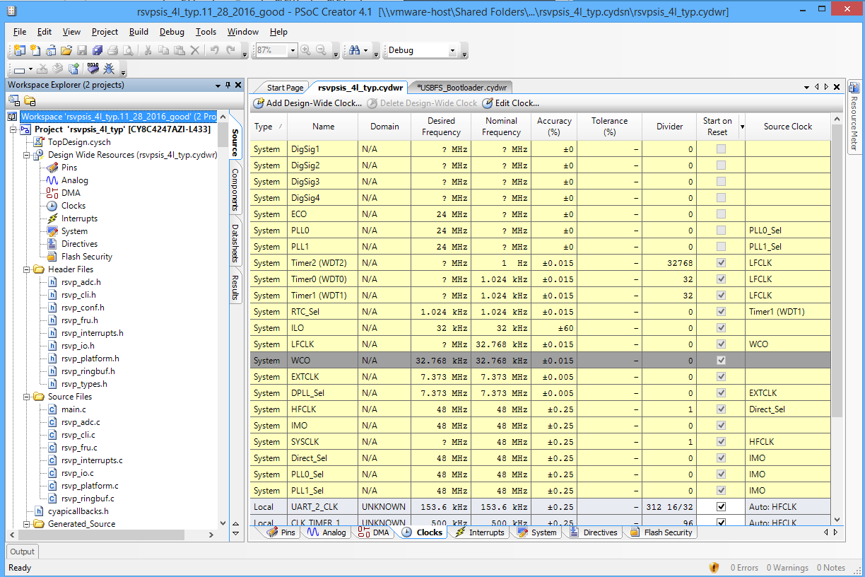
To explain why we are stuck there you first need to double click on the “Clocks” tab in the Design Wide Resources.  When you do that it will take you to this screen which contains a bunch of information about the clocking system in the PSoC.

PSoC4 Clock Setup

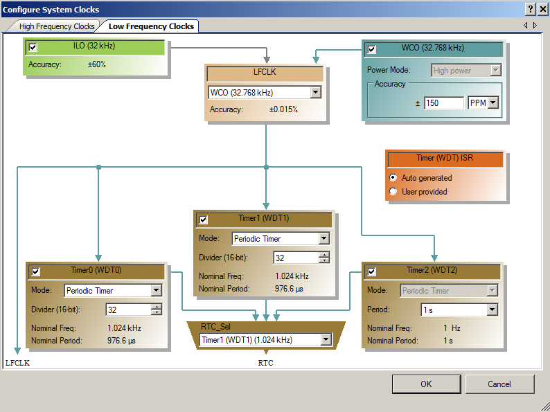
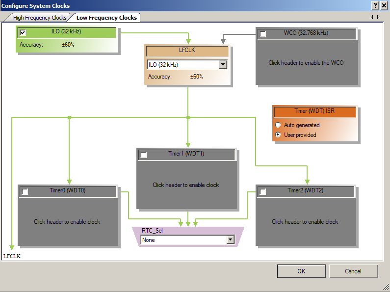
In the screen above, you can see that there are three Timers in the Watch Dog Timer system (WDT) that are clocked (i.e. have a Source Clock of) by the Low Frequency Clock (LFCLK).  The LFCLK has its source as the Watch Crystal Oscillator (WCO).  If you double click the WCO line it will take you to a screen that is much easier to see what is going on, specifically the “Configure System Clocks” screen:

PSoC4 Clock - Low Frequency

In the screen above you can see that the LFCLK has two choices of oscillator sources, the “ILO” or the “WCO”.  ILO stands for Internal Low Speed Oscillator.  The ILO is a fairly inaccurate (+- 60%) RC oscillator that is built inside of the chip.   It is designed to be very low power which is why it is so inaccurate.  If you need a more accurate oscillator, then you should use an external oscillator, specifically a Watch Crystal Oscillator or WCO.  A WCO is a 32.768KHz crystal oscillator.  These watch crystal oscillators give you very precise clocks that can be used to drive real time clocks accurately.

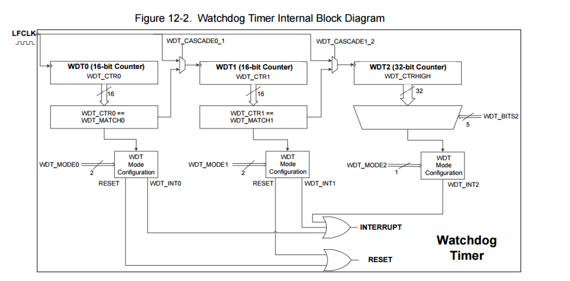
The next thing to see is there are three Watch Dog Timers (WDT) numbered 0-2.  These times are driven by the “LFCLK”.  Here is a picture from the PSoC Technical Reference Manual.


PSoC4 Clock - WDT Block Diagram

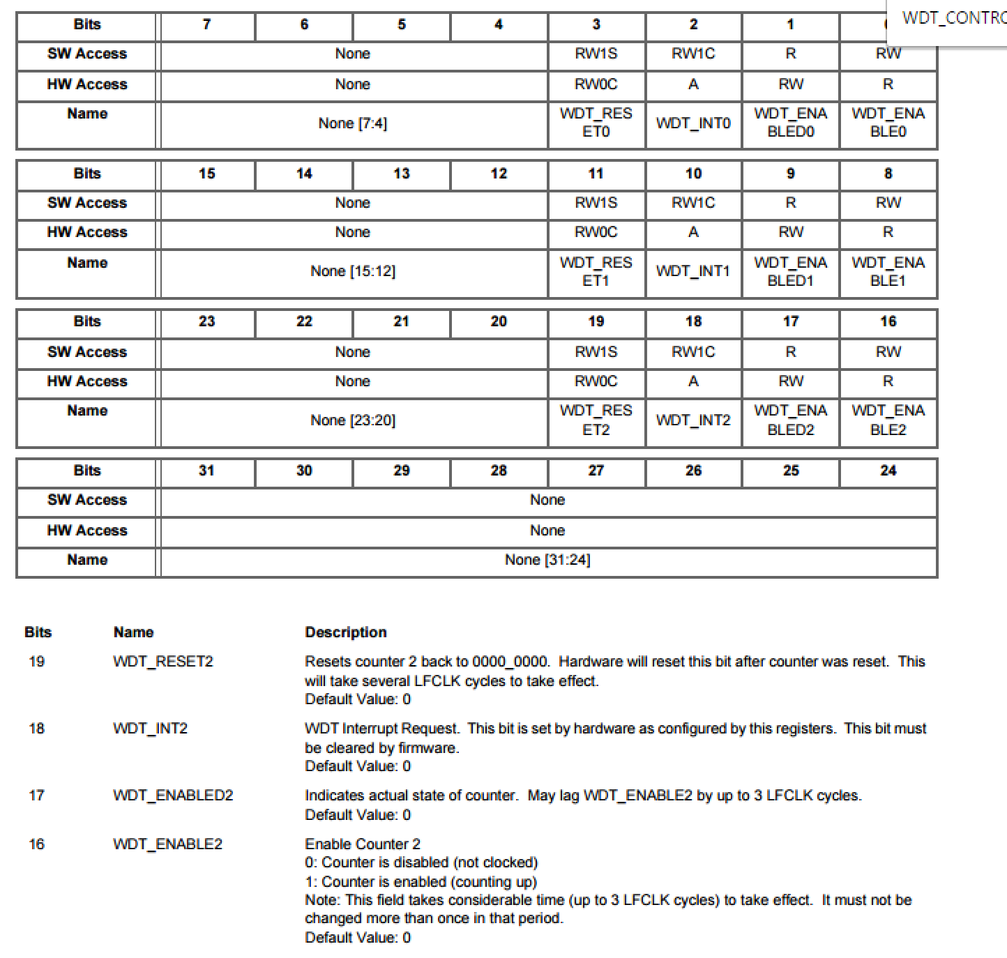
So what is the “CYREG_WDT_CONTROL”?  You can find that by looking in the PSoC4 Registers TRM.

PSoC4 Clock WDT Control Register

The busy wait loop is waiting for bits 19,11,3 to be cleared.  Those bits are “WDT_RESETx”  They become 0 when the three WDT timers are cleared which happens “several LFCLK cycles” after the reset.  As a reminder, here is that block of code:

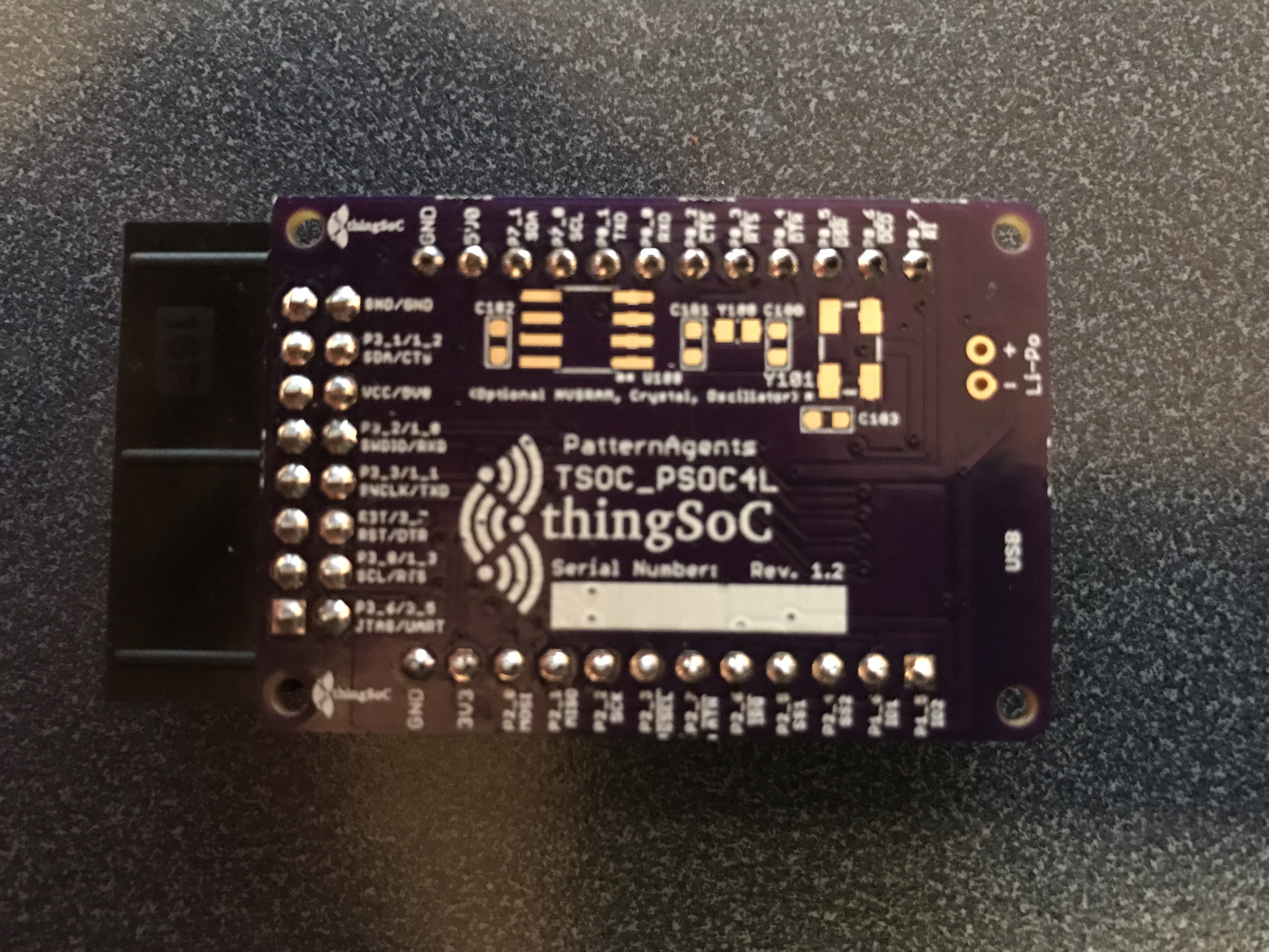
This still leaves us with the question, “What is the problem?”.  If you look on the back of the ThingSoC4L board you will see there is no Crystal populated on this board. (the blank footprint on the right side of the back).  The WCO is an optional feature from Pattern Agents.  If you need the more accurate timing, you need to solder on your own Crystal.

Backside of ThingSoC4L PCB

If there is no WCO crystal, then the WDT timer reset will never happen because LFCLK isn’t doing anything.  And, the busy wait loop will never end.  Mystery solved.

The Pattern Agents Bug Fix

To fix the startup problem, the Pattern Agents guys changed the clock configuration to

  1. Turn off the WDTs
  2. Use the ILO as the source of the LFCLK

PSoC4 Clock - Low Frequency Setup

You can find all of the projects in the TSoC Series at my GitHub ThingSoC repository git@github.com:iotexpert/ThingSoC.git

Index Description
ThingSoc: TSoC PSoC4L Development Kit from PatternAgents Introduction to ThingSoC
ThingSoC PSoC4L: Using & Debugging the PSoC4 Clock Debugging a beta firmware problem
ThingSoC: The TSoC GROVEY I2CHUB : I2C Hub/Switch Evaluating the ThingSoC I2C Hub
ThingSoC: Multiple I2C Displays Using the I2CHUB and U8X8 Library A project using ThingSoC I2C Hub & 4 OLED Displays

ThingSoC: TSoC PSoC4L Development Kit from PatternAgents

Pattern Agents are running a crowd funding effort for ThingSoC TSoC4L … help them here

Summary

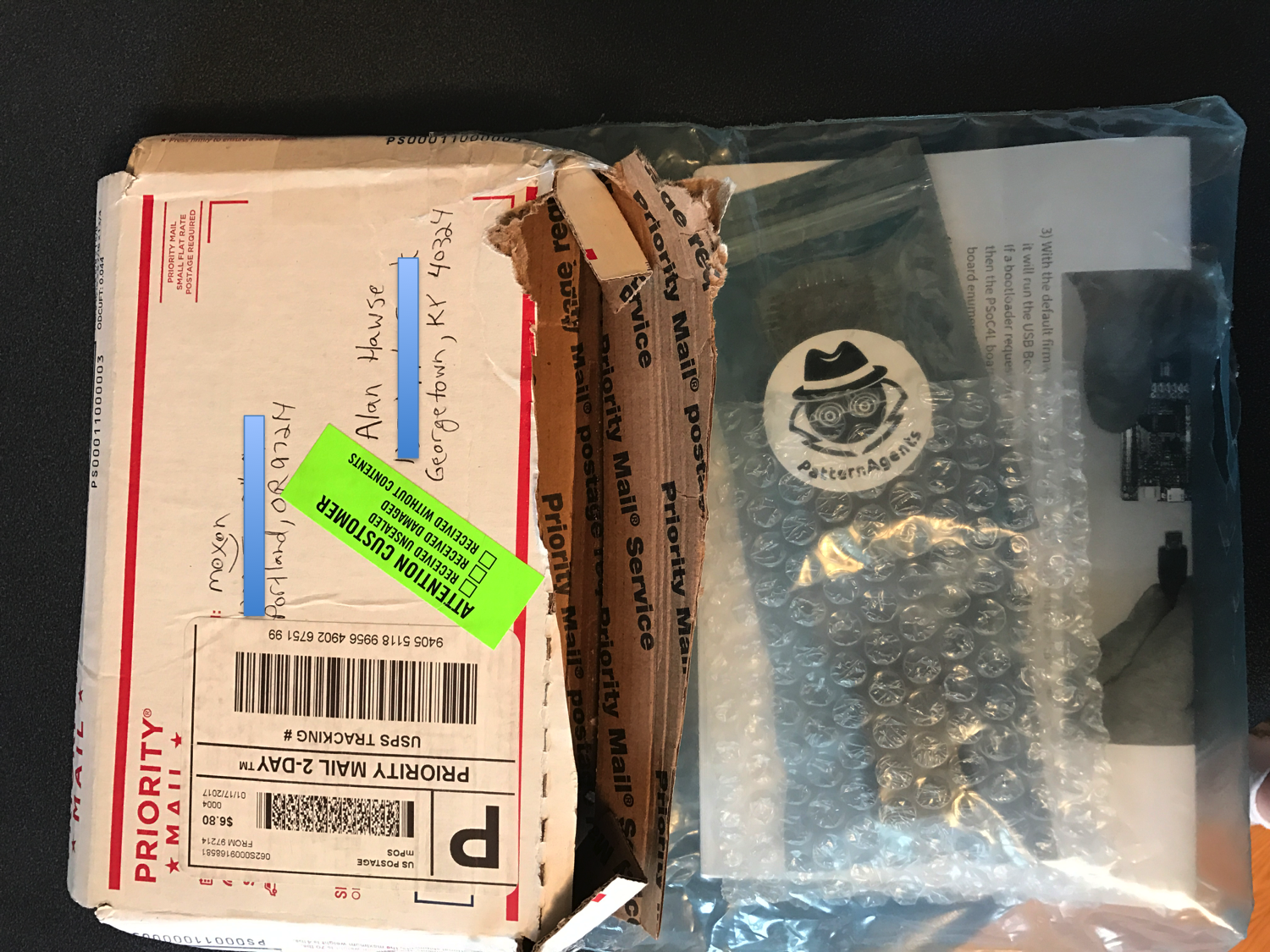
Last week I got a box in the mail from my friend Tom Moxon in Oregon.  He runs a company called Pattern Agents.  I was excited when I saw the box because I love new development kits.  I was even more happy when I opened the box and found a ThingSoC PSoC4L kit.

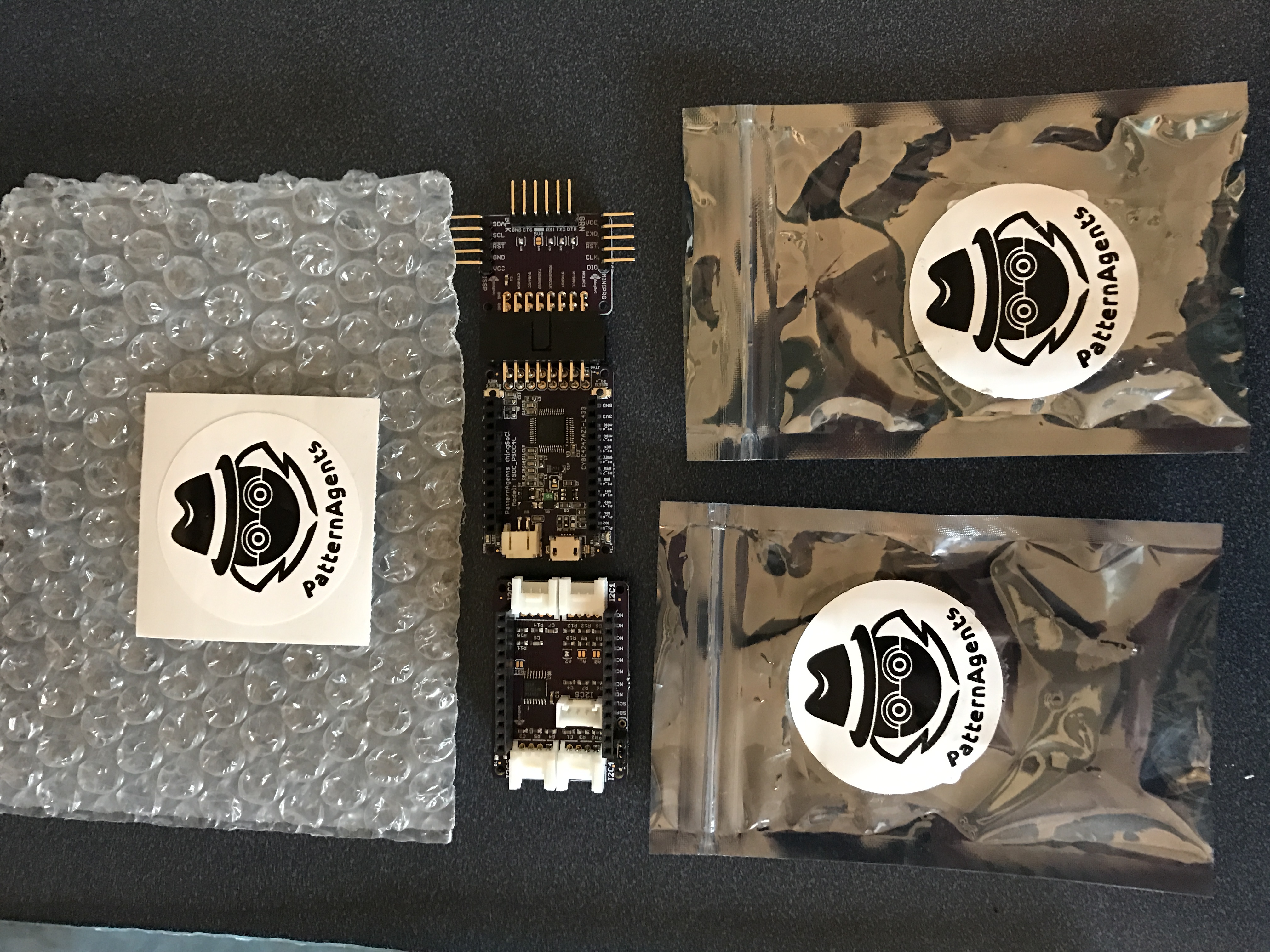
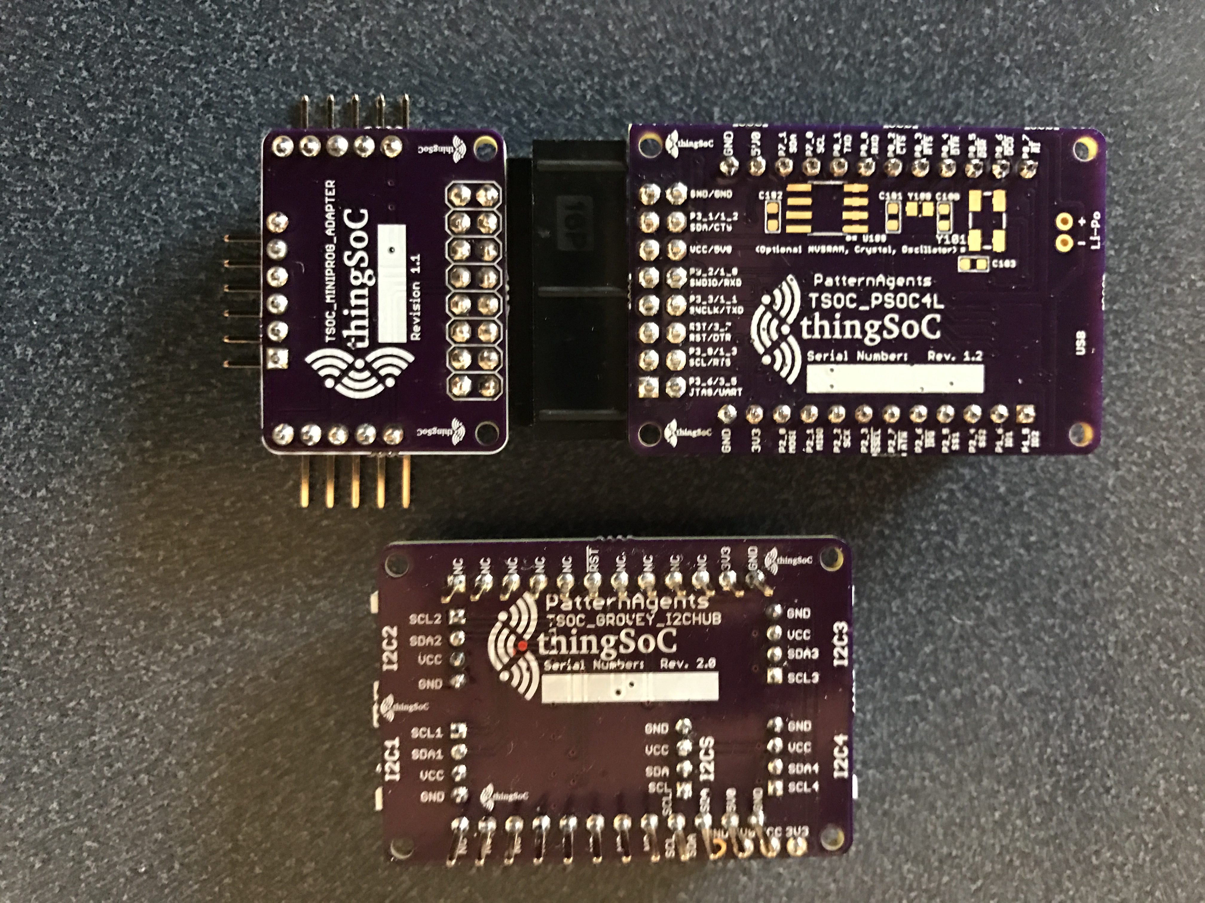
Tom sent me three boards

  1. A ThingSoC PSoC4L
  2. A MiniProg Adaptor
  3. A ThingSoC I2C Hub

ThingSoC PSoC 4L Packaging

ThingSoC PSoC4L

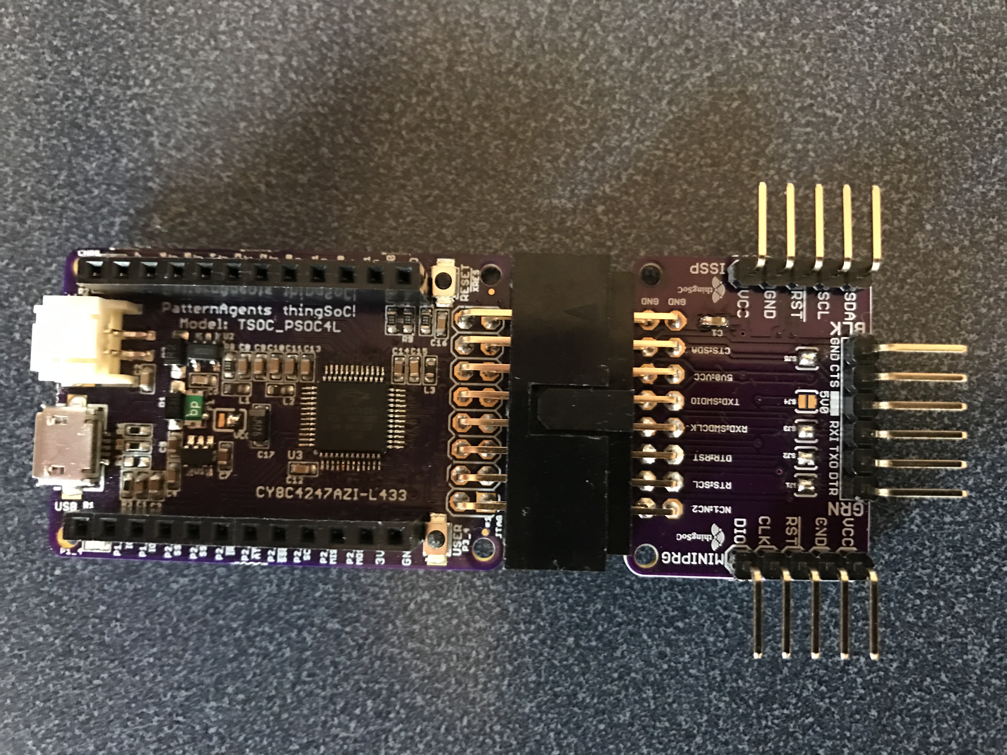
The ThingSoC complies to a new open source stackable footprint called the ThingSoC Open Source Socket.  This ThingSoC board is driven by a PSoC4L.  The PSoC4L is the largest and most capable of the PSoC4 family.  This chip “completed” the high end of the PSoC4 family by adding more IOs, more Flash, more RAM and a USB controller.  The PSoC4L serves as the base MCU in the stack as well as providing a bridge to the PC via a USB <–> UART Connection.  The board also has a connection for a 3.7V LiPo battery to power the system.  In the picture below you can see the base board (on the left) with the programmer attachment (on the right).  The programmer attachment lets you attach a MiniProg-3 or a Uart Bridge or an ISSP connection (like a MiniProg-1).

thingsoc 4200l

Here is a picture of the backs of the boards.  On the back of the ThingSoC PSoC4L board you can see a place to solder a Cypress NVSRAM as well as a footprint for a Watch Crystal.

The backs of the ThingSoC PSoC4L

The Blinking LED

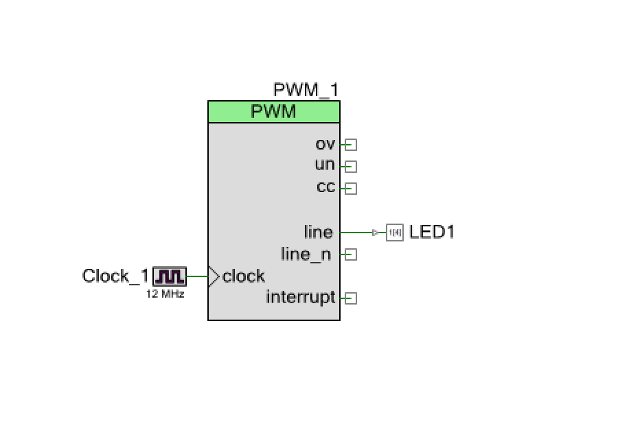
The first thing I did with the board (and no, reading the instructions wasn’t the first thing) was program the chip to blink the LED.  Obviously with a PSoC the best thing to do was make a schematic with a PWM driving the USER LED pin:

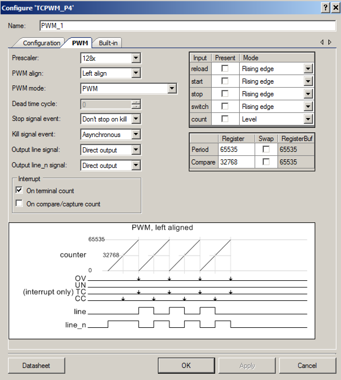
I used the default clock of 12MHZ, then I used the PWM pre divider to get the frequency down to something that I could see.

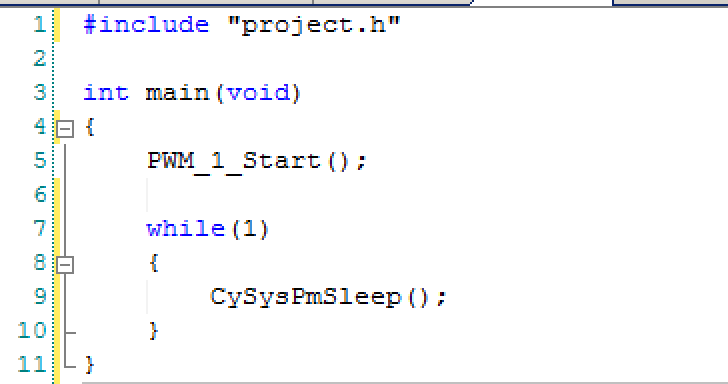
Lastly, I wrote a tiny bit of firmware to get things going.  Notice that I use the CySysPmSleep to put the CPU to sleep.  It never wakes up from this sleep (because there are no interrupt sources to wake it up).  But, if it did, it would go right back to sleep because of the loop.

After programming the board, the LED started right up.  That is good as it means everything makes sense.

When I programmed the Blinking LED project I overwrote Tom’s default firmware which is called “RISC”.  In the next post Ill talk more about the architecture of the ThingSoC PSoC4L.

You can find all of the projects in the TSoC Series at my GitHub ThingSoC repository git@github.com:iotexpert/ThingSoC.git

Index Description
ThingSoc: TSoC PSoC4L Development Kit from PatternAgents Introduction to ThingSoC
ThingSoC PSoC4L: Using & Debugging the PSoC4 Clock Debugging a beta firmware problem
ThingSoC: The TSoC GROVEY I2CHUB : I2C Hub/Switch Evaluating the ThingSoC I2C Hub
ThingSoC: Multiple I2C Displays Using the I2CHUB and U8X8 Library A project using ThingSoC I2C Hub & 4 OLED Displays

Pinball: Testing the Eagle PCB

Summary

In the previous post I talked about my process for assembling the Pinball PCB.  In this post I will take you through all of the steps that I took while testing the Eagle PCB functionality.  I have not yet written the full Pinball game firmware, so I used a small test program, an Oscilloscope and a multimeter to test each of the subsystems.  In order these are the systems that i tested:

  1. Power Supply
  2. I2C OLED LCD Screen
  3. CapSense (creator bug)
  4. Buzzers
  5. Motor Driver
  6. LEDs
  7. Switches
  8. Accelerometer
  9. Bluetooth

Test the Power Supply

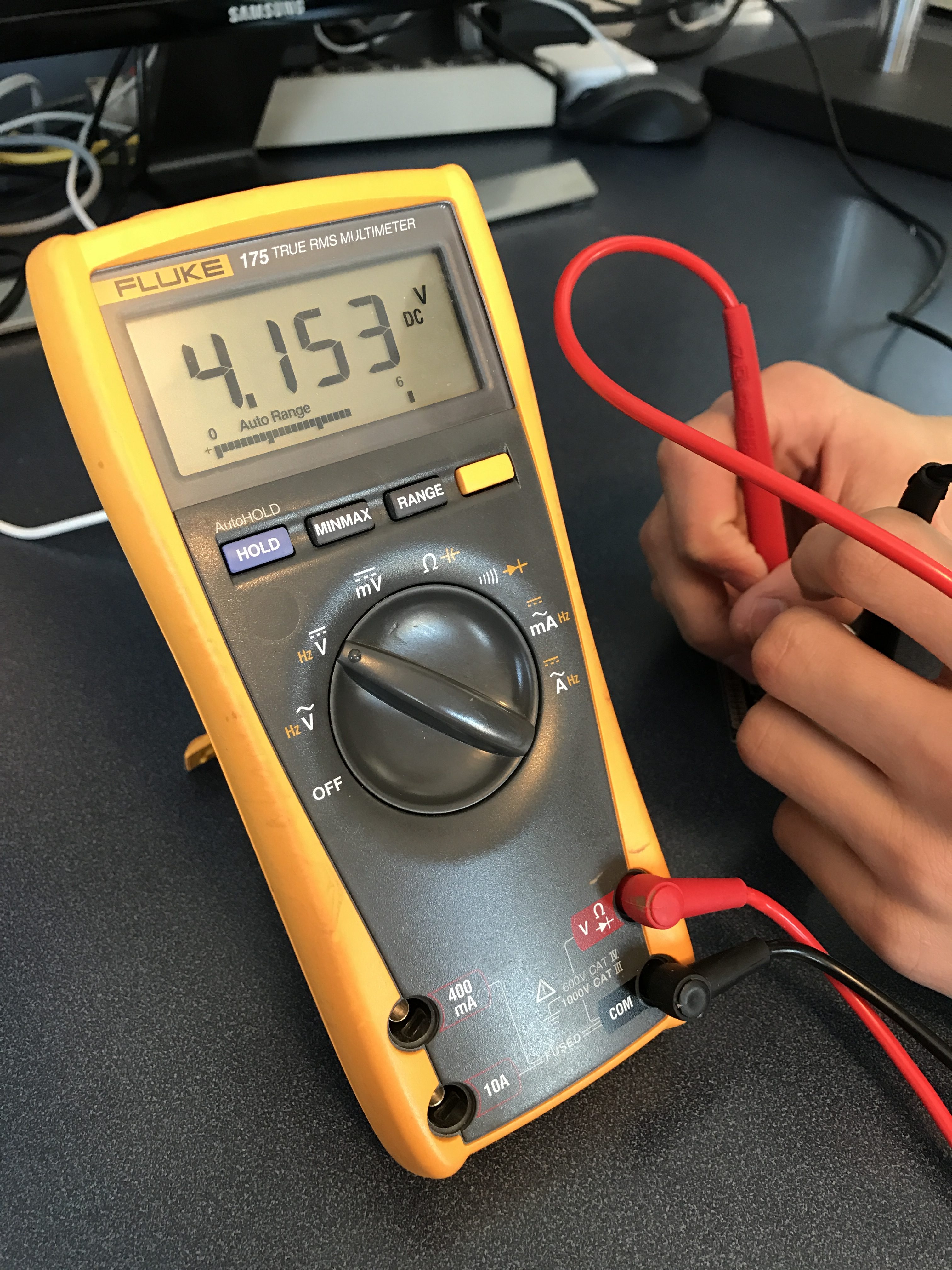
My first step was to plug in the Eagle PCB and see what happens.  There was no smoke, but when I measured the power supply I got this:

fluke power supply measurement

Not perfect and I wondered why I got 4.1v instead of 3.3v.  But, the system will work at 4.1v so I deferred solving the problem until later.  [Edit: It turns out that I did something really stupid and then got lucky.  I will post soon about exactly what happened and how I fixed it.]

Test the OLED LCD Screen

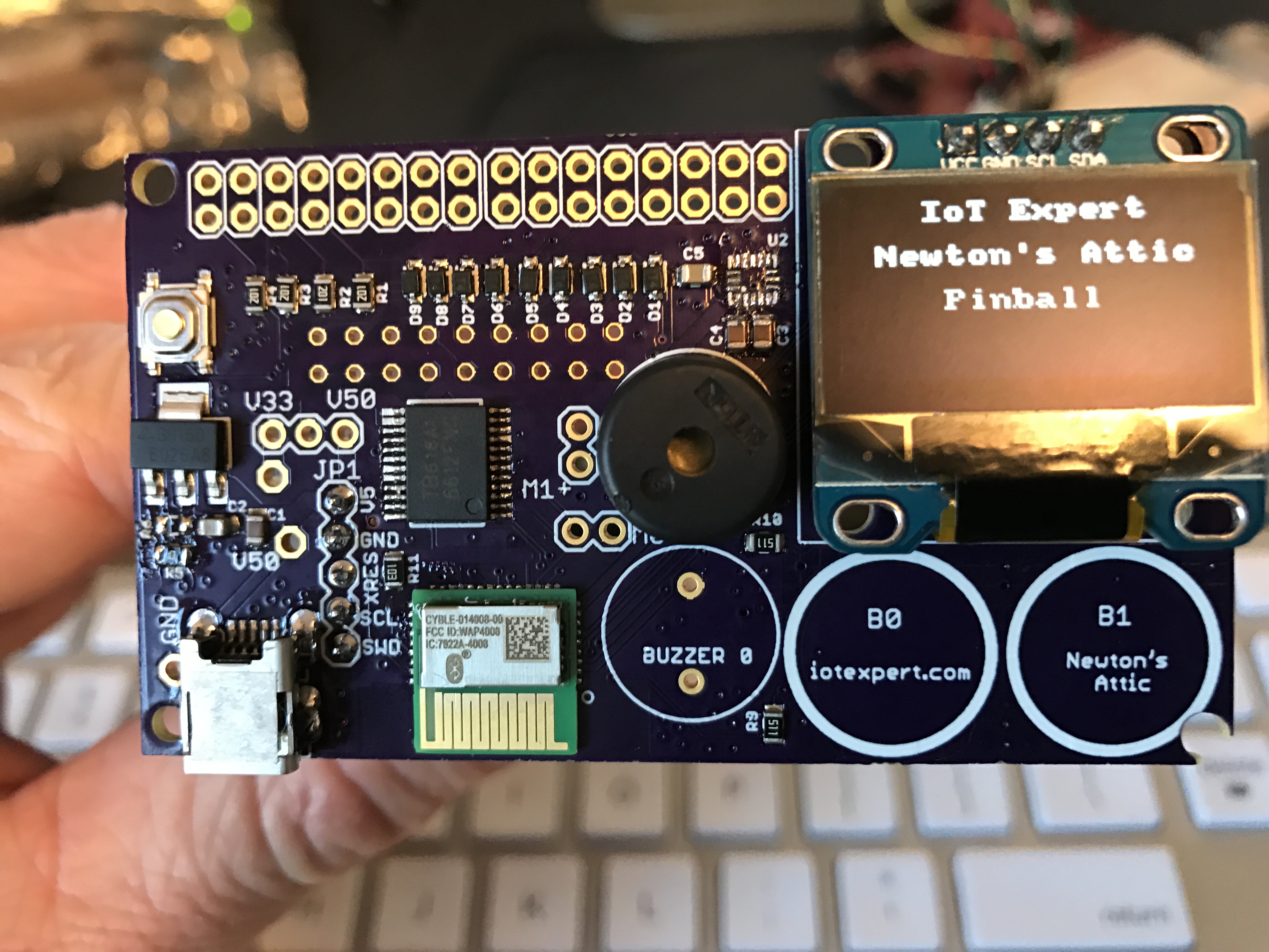
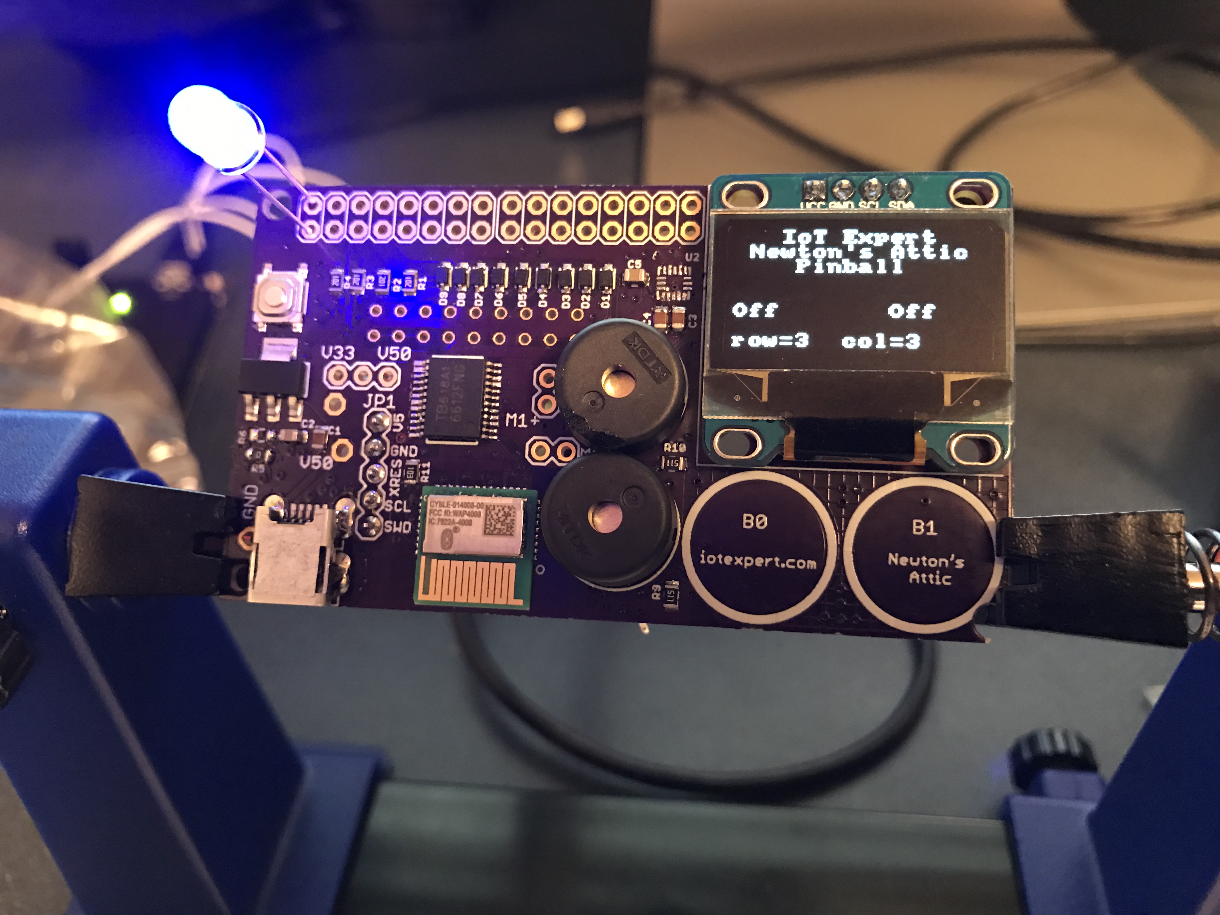
Before I soldered in the LCD display, I decided to measure the I2C pins to make sure they were what I was expecting.  Unfortunately, when I measured them, I had about 800 ohms of resistance between the VCC and Ground which didn’t make a bit of sense.  To make matters worse the SDA and SCL were essentially shorted to ground.  After thinking about it for a while, I decided that the most likely culprit was the QFN accelerometer (which is also attached to the I2C bus).  That tiny little chip, with no-visible leads and 0.5mm pitch pads is an absolute beast to solder (more on this problem in a future post).  The accelerometer looked “OK”, but I decided to remove it anyway using my hot air tool.  As soon as I got it off the board I could see a big blob of solder on the pads.  After I cleaned up the blob of solder with a copper braid and soldering iron, I retested all of the pins.  They were now fine.  So I went ahead and soldered the display into the board (which also turned out to be a bad idea).  You can see the (unpopulated) accelerometer footprint just to the left of the display.

OLED Screen Test

To test the display I ported Oliver Kraus’ U8G2 library to the PSoC.  This library lets you use an I2C to interface with a bunch of different small OLEDs.  You can read more about using the display in a future post.  Here is the block of code that makes the display work:

Test the CapSense

PSoC CapSense Test

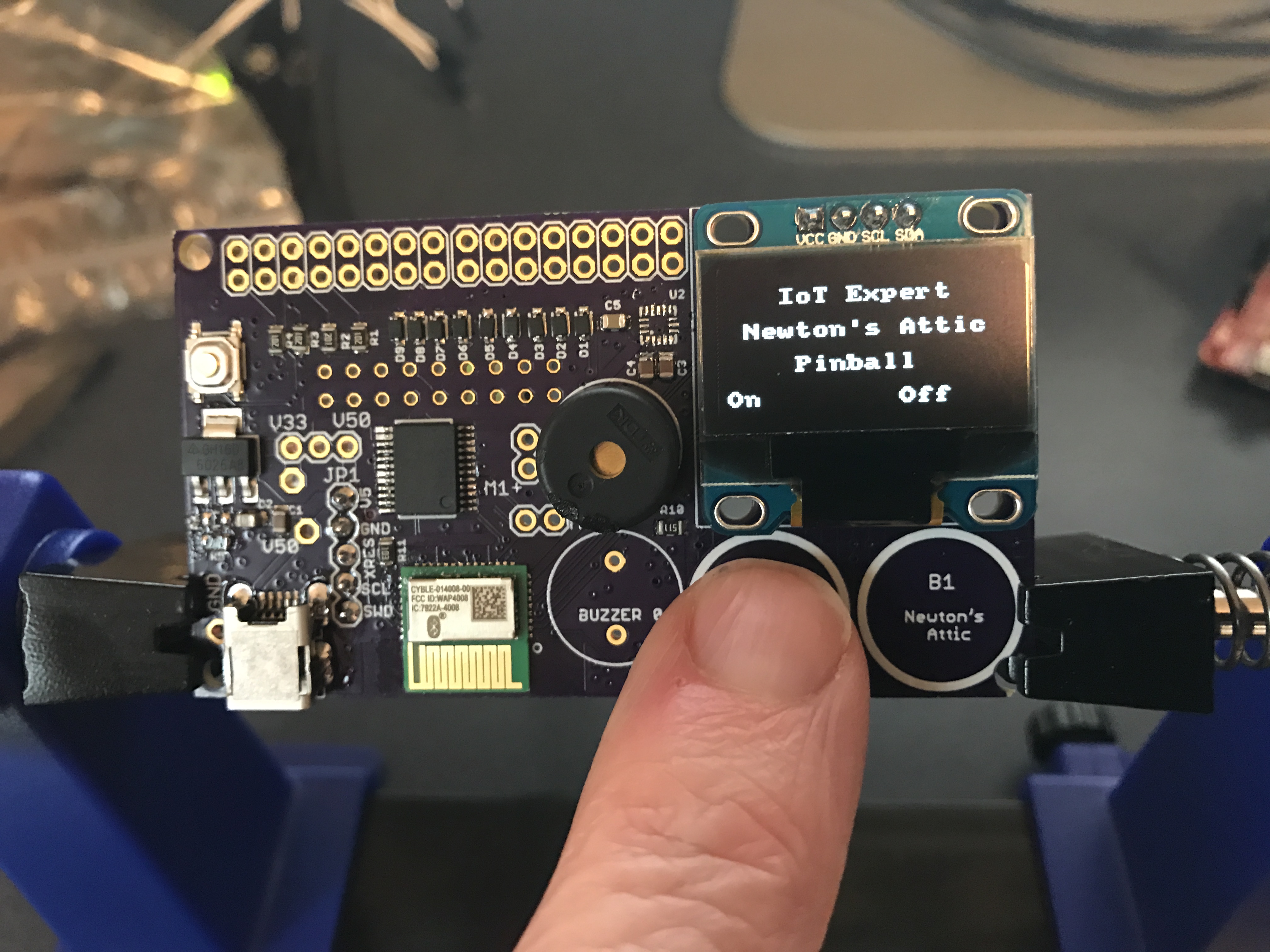
In order to test the CapSense buttons I wrote a simple block of firmware to read the state of the buttons and display that state on the screen:

Test the Buzzers

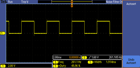
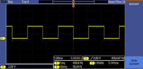
In order to test the buzzers, I just connected them to the PWMs and drove a square wave of 262Hz and 440Hz.

Buzzer 0 PWM Test

Buzzer 1 PWM Test

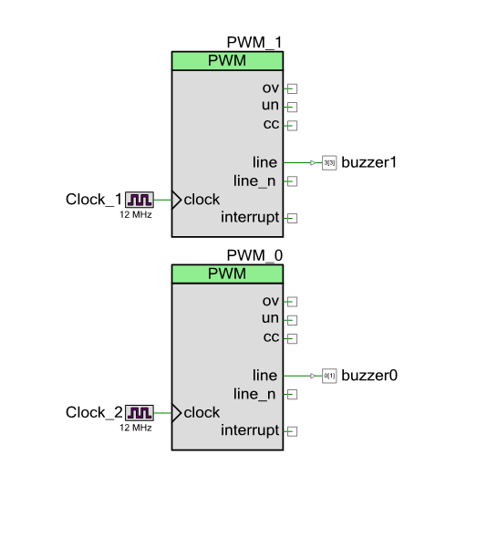
Here is the schematic for that circuit:

Buzzer PWM Test Circuit

Test the Motor Driver

In order to test the motor drivers, I used a PWM to drive a 50Hz Square wave onto the output.  Unfortunately, I got this:

Motor Driver Oscilloscope Measurement

Something is wrong.  When I first saw this waveform I wasn’t too happy.  But after doing some digging I figured out how to fix it.  This will be the subject of an upcoming post.  The good thing about this waveform is that my daughter, Anna, is studying exponentials functions in Calculus right now.  She recently asked me if there was an useful application of f(x) = e^x.  This was a perfect way to show her a practical application of a differential equation.

Test the LEDs

To test the LEDs I used the switching LED matrix component program that I showed in an earlier post.  To make things easier, I just stuck an LED in each pair of holes to make sure that they were working.  Here is a picture:

Matrix LED Test

Test the Switches

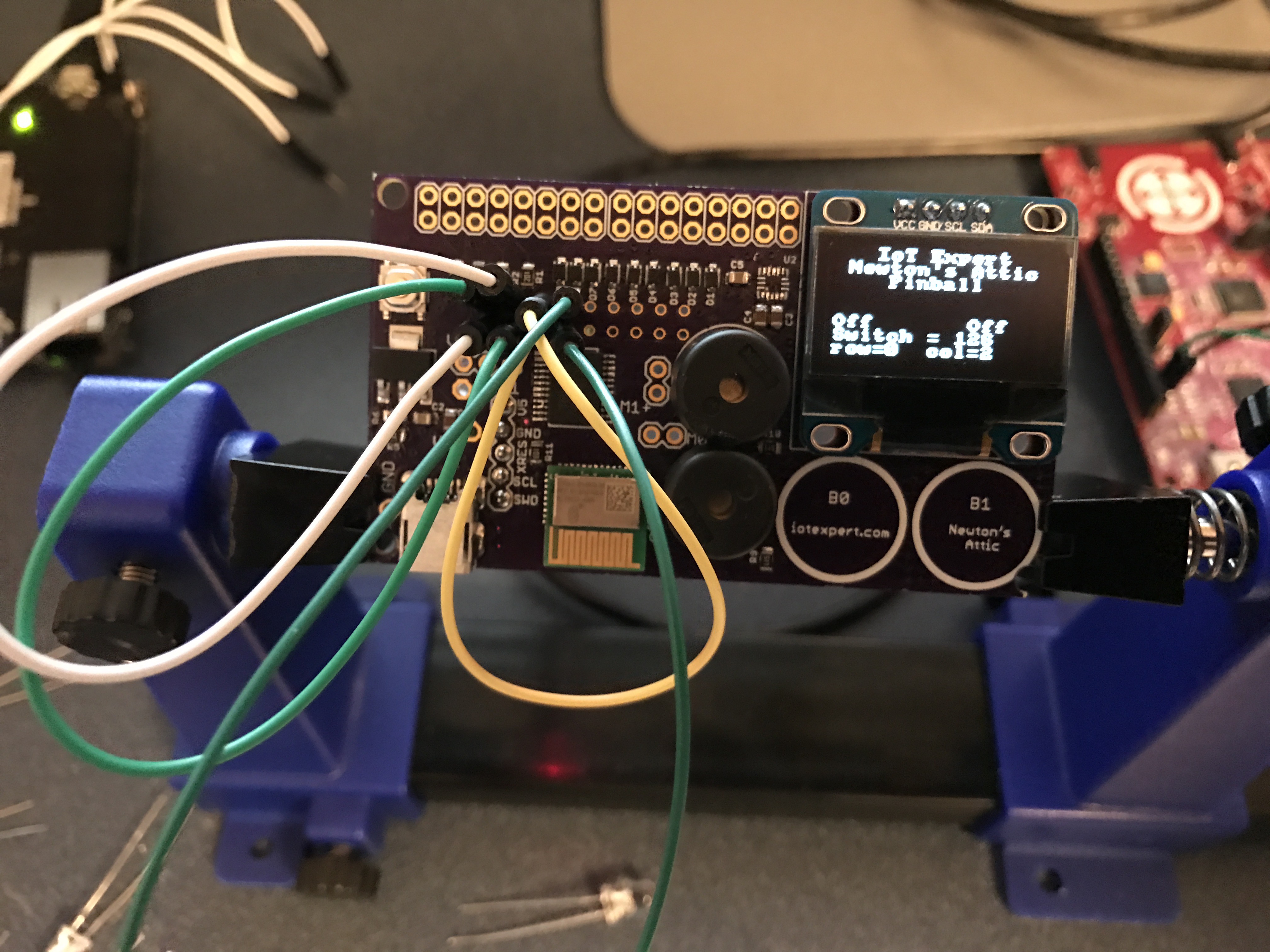
To test the switches, I used the Switch Matrix Component that I talked about in detail in a previous post.  In order to see the switches in their on state, I just plugged in a wire.  Here is a picture of a few of them being tested.

Switch Matrix Component Test

Test the Accelerometer

As I mentioned earlier in this post, the accelerometer had a big nasty blob of solder under it which shorted SDA/SCL to ground.  I am going to dedicate an entire post to fixing this problem.

Test the Bluetooth

The very last sub-system to test is the Bluetooth.  I decided to put in enough firmware that the device could:

  1. Advertise
  2. Disconnect
  3. Restart advertising

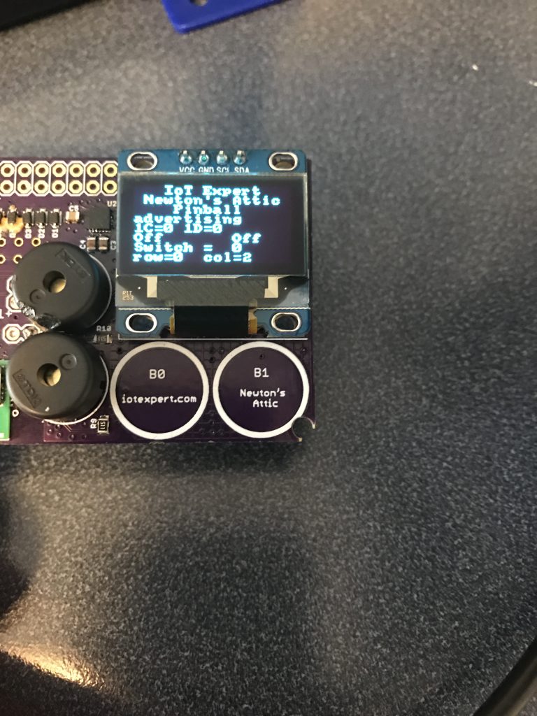
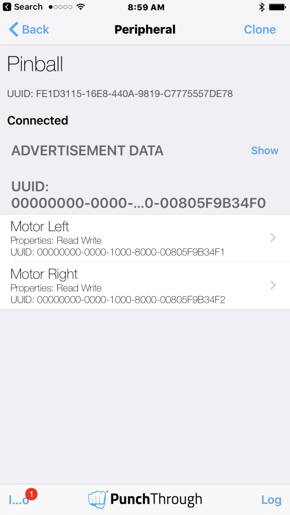
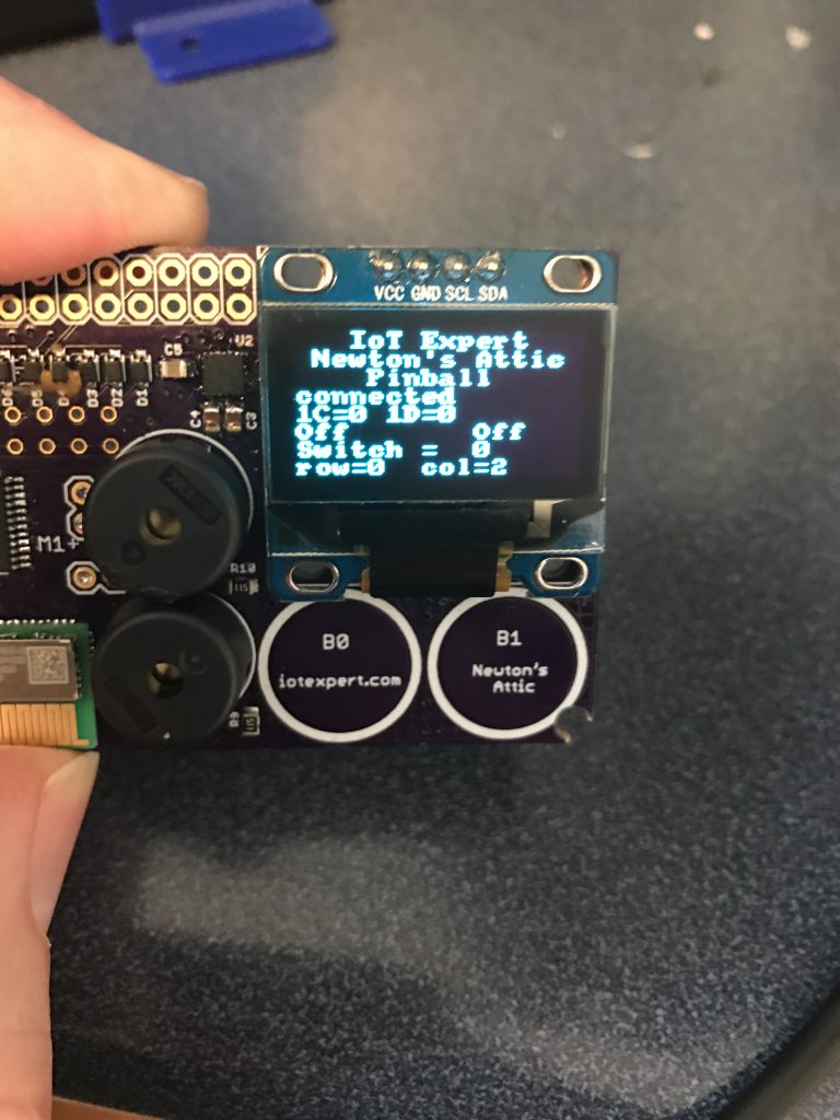
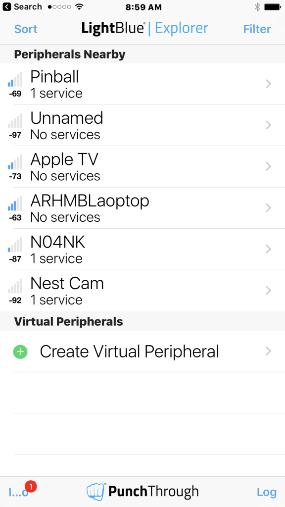
And display all of that on the OLED.  Here is a picture:

OLED Display showing BLE Advertising State

iPhone Light Blue BLE Browser Showing Advertising Devices

Bluetooth Advertising Test

Light Blue BLE GATT Database Explorer

You can find all of the source code and files at the IOTEXPERT site on github.

Index Description
Pinball: Newton's Attic Pinball An introduction to the project and the goals
Pinball: Lotsa Blinking LEDs Everyone needs a bunch of LEDs on their Pinball Machine
Pinball: Matrix LEDs (Part 1) Saving PSoC pins by using a matrix scheme
Pinball: Matrix LEDs (Part 2) Solving some problems with the matrix
Pinball: Matrix LEDs Component How to turn the Matrix LED into a component
Pinball: A Switch Matrix Implementing a bunch of switches
Pinball: Switch Matrix Component (Part 1) The switch matrix component implementation
Pinball: Switch Matrix Component (Part 2) The firmware for matrix component
Pinball: Switch Matrix Component (Part 3) Test firmware for the matrix component
Pinball: The Music Player (Part 1) The schematic and symbol for a Music Player component
Pinball: The Music Player (Part 2) The Public API for the Music Player component
Pinball: The Music Player (Part 3) The firmware to make the sweet sweet music
Pinball: The Music Player (Part 4) The test program for the music player
Pinball: The Motors + HBridge Using an Bridge to control DC Motors
Pinball: The Eagle Schematic All of the circuits into an Eagle schematic
Pinball: The Printed Circuit Board 1.0 The first Eagle PCB layout of the printed circuit board
Pinball: The PCB Version 1.0 Fail Problems with the first version of the Eagle PCB layout
Pinball: PCB Layout 1.2 Updates using Eagle Fixing the errors on the first two versions of the Eagle PCB
Pinball: Assemble and Reflow the 1.2 PCB Assembling the Eagle PCB
Pinball: Testing the Eagle PCB Firmware to test the newly built Pinball printed circuit board
Pinball: Debugging the Motor Driver Fixing the motor driver PSoC project
Pinball: Hot-Air Reworking the Accelerometer Solder Using a Hot-Air Rework tool to reflow a QFN
Pinball: Debugging the LM317 Power Supply- A Tale of Getting Lucky Debugging the LM317/LM117 power supply
A New Logo Design Contest for IoT Expert (Part 1)

IoT Expert Logo Design Contest

When I created this blog, I looked around at a bunch of different websites.  After seeing what was out there, I bought a fairly plain WordPress theme, put it online, then started typing blogs.  This situation has been OK, but not ideal.  I realized last fall that I needed to do better.  But what?  I didn’t really know, nor have time to think about it.  Then in December, my friend John Turbek, sent me an email invitation to participate in a logo design contest for his boutique farm Fertile Pastures.

He was running a logo contest using a company called 99designs.com.  This company is associated with a bunch (like 100,000) of free lance designers.  You can create a design contest by describing what kind of things you like and what you are trying to do.  Then designers from all over the world submit their ideas.  You can refine the designs as part of a 2 stage design contest.  At the end you pick a winner, the designer gets paid, and you end up with a copyright for your new logo as well as the artifacts from the contest.

I thought that this would be an easy way to get what I needed for this website.  Turns out, I got what I needed, but it wasn’t easy.  The 99designs website works very well, but it was incredibly time consuming to look a the 724 designs that were submitted and rank/rate them and their creators.  Apparently, IoT is an interesting subject (who knew?) and I had an abnormally large number of designers and submission for my contest.  There were a bunch of really cool ideas and interesting people.

First, the winner is Ceasar Cuervo (not Jose).  Here is a link to his website. which has a bunch of really cool examples of his designs.  Here is his winning design:

I agonized for several days about the end result for the logo design contest as there where three other designers who stood out.  I was sorry not to choose them because they seemed to capable and creative.  I would recommend any one of them.

The best of the finalists was Ann Sir.  He has a super cool website with his portfolio.  I was very close to choosing this design as the winner because I thought that in many ways it the most creative.  Here is his design, which even now,  I am sad that I didn’t choose.

Ann Sir logo design contest submission

The next person is Ivek_design.  Ivo lives in Croatia and has won a bunch of these contests.  I thought that his submission to the new logo design contest was really creative.  Moreover, he “gets it” and I found him to be very responsive an intelligent.  Here is the Ivek Design:

Ivek Design logo design contest submission

The final person who I really liked is Kaylee CK.  Ms. Kalee CK was by far the most prolific of the designers who submitted to the new logo design contest.  She is super responsive and was the source of many many ideas that I thought were clever.  She is also a “go-getter” type and has won a bunch of these contests.  Here is one of her many designs which I also think is very clever.

Kaylee CK logo design contest submission

In an upcoming post, Ill talk about the whole process that I followed to get this chosen and deployed.

Pinball: PCB Solder Reflow the OSH Park – Eagle 1.2 Board

Summary of my PCB Solder Reflow Process

Getting the purple envelope from OSH Park is always exciting.  The big question is,  “After all those hours studying the Eagle PCB editor, did I make the same error three times in a row, or did I finally get it right?”  In this post, I will take you through all of the steps that I follow in in my PCB reflow solder assembly process.  I use a Qinsi QS-5100 PCB Solder Reflow Oven which I talked about in detail in a previous post.  One of the interesting things about this blog website is that it has driven me to write down some of my procedures and move away from the “just wing it” method.  I believe this will pay long term dividends for me.  So, Thank You!

My board assembly process is as follows:

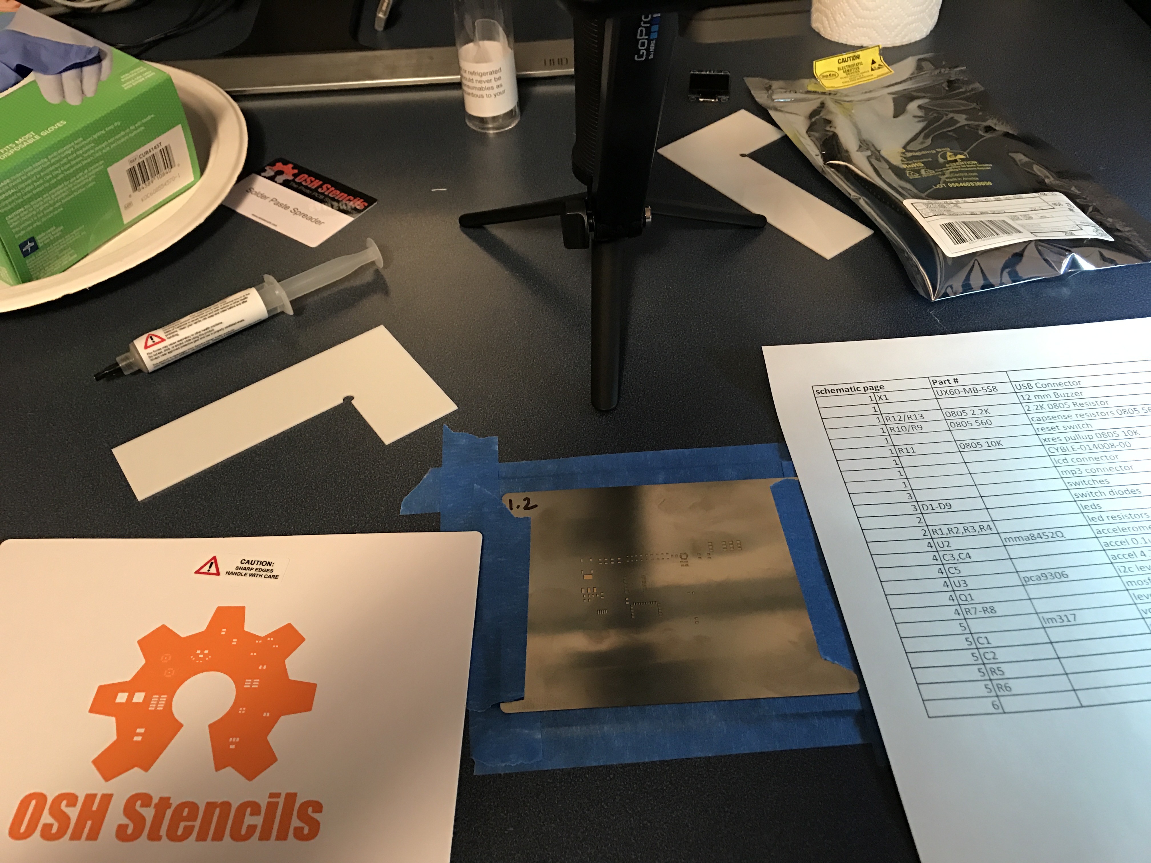
  1. Take solder paste out of the refrigerator and let it warm up (probably at least 2 hours)
  2. Test fit the through hole and major surface mount components
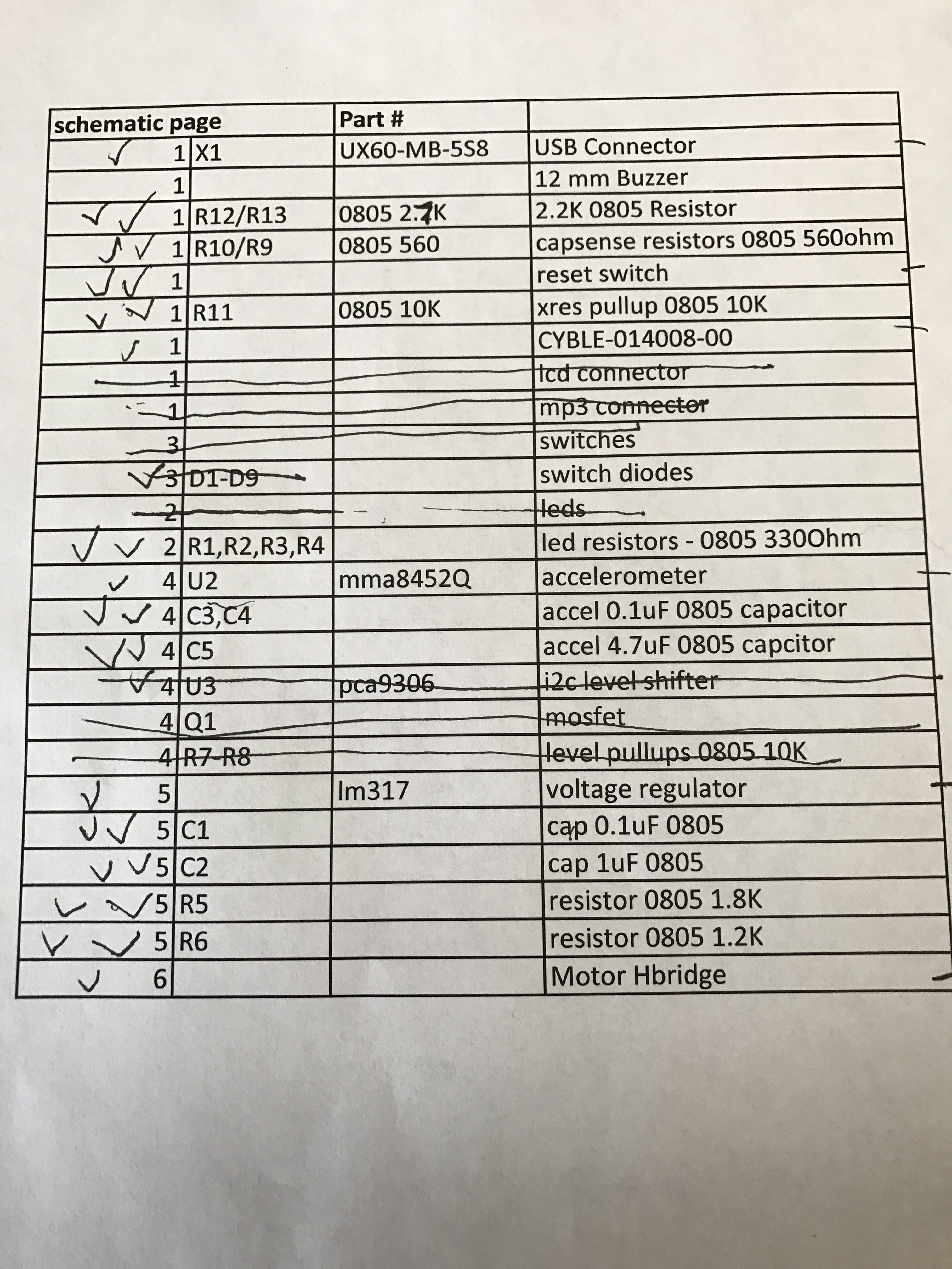
  3. Print out the parts list to use as a checklist
  4. Setup all of the parts on the desk in some order (using checklist)
  5. Tape the board holders to the desk
  6. Make sure the solder stencil registers correctly
  7. Screen on the solder paste (video)
  8. Inspect the solder paste with a microscope
  9. Place all of the parts
  10. Reflow the PCB in the Qinsi QS-5100 oven
  11. Visually inspect the solder and clean up any solder balls
  12. Solder in the programmer connector and program the board
  13. Cleanup the disaster area

Take the Solder Paste out of the Refrigerator

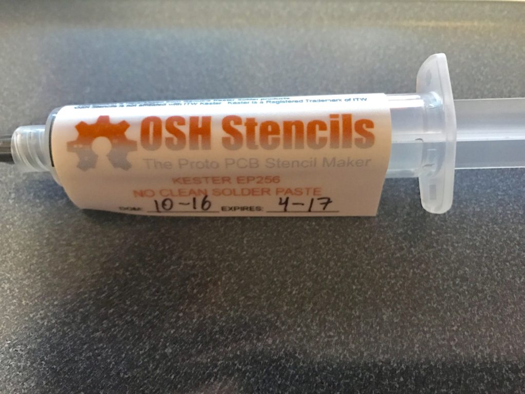
You need to have solder paste at room temperature as cold solder paste does not spread very well.  I recommend that you take the solder paste out of the refrigerator at least two hours before you use it.  I use Kester EP256 solder which comes in a syringe or a tub.  In this case, I purchased it from OSH Stencils when I bought the original stencil.  In two of the videos I watched on the internet, the person put extra solder back into the tub but obviously that cannot be done with a syringe.  My experience has been that older solder paste that has been exposed to air will not reflow properly.  That will make you crazy, and is the reason why I have not gone down the road of saving extra solder.  I cannot emphasize enough to keep your solder cool and fresh.

Test Fit Components onto the OSH Park /Eagle PCB

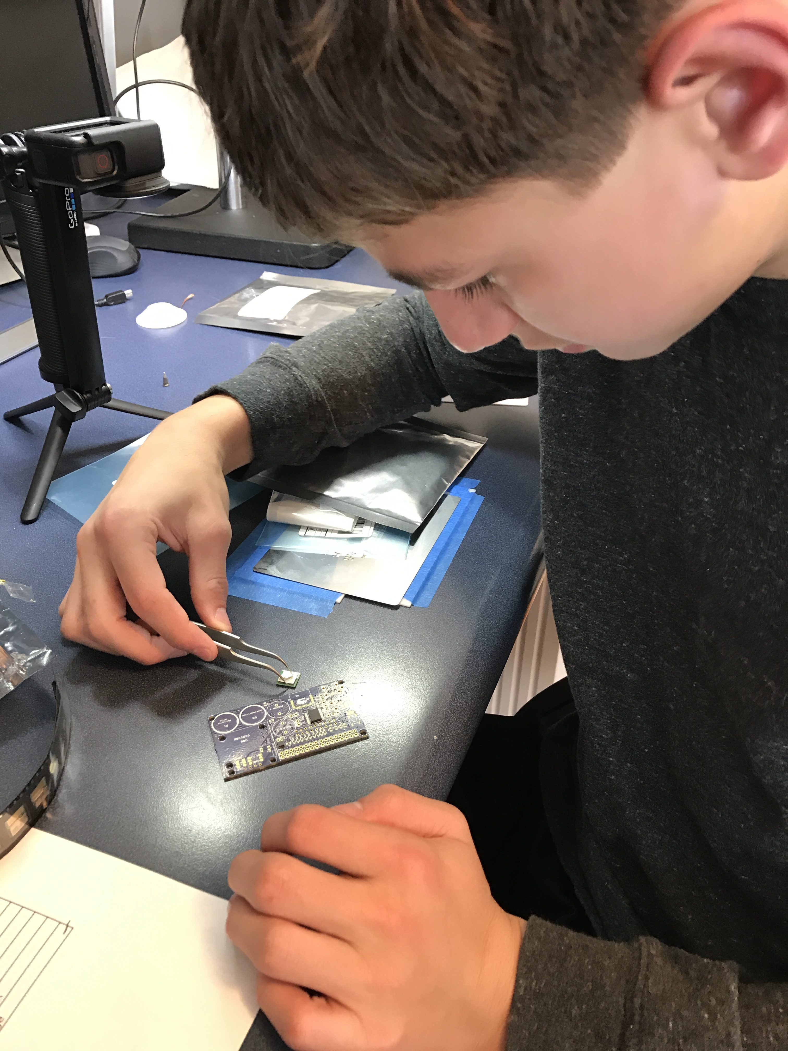
When I get a new board, the first thing that I do is make sure that the major parts align to their footprint.  You don’t want to get down the road with paste on your PCB and find that you screwed up the size or placement of a component.  Here is a picture of my lab assistant test fitting the PSoC.

Parts Checklist

While I am designing the PCB in Eagle I always create a BOM spreadsheet with the names of the parts, the part number, the label on PCB silkscreen, etc.  I use this spreadsheet to ensure that I have all of the parts available to put on the board.  It sucks to get a PCB with solder paste on it, then be missing a part that you need.  Moreover, you need to move reasonably quickly once you have paste on the board (or the paste will harden) so making sure you have everything at hand is critical.

Setup all of the parts on the desk in some order

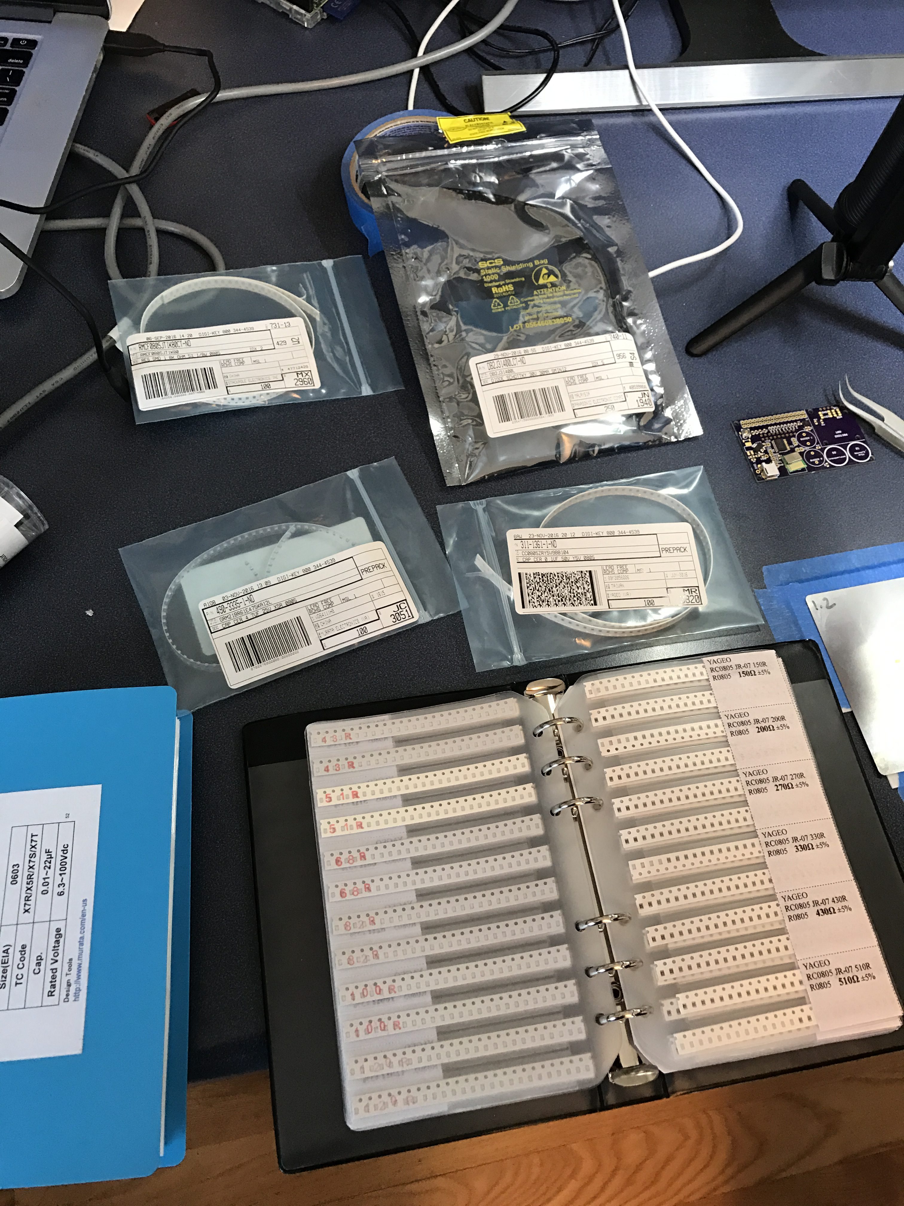
For some strange reason, it always feels stressful placing the parts onto the PCB.  In order to make the process smoother, I arrange the parts on my desk in some order.  In this case, all of the parts are by type i.e the resistors are all together.

Tape the PCB Brackets onto the Table

Once I have things setup, I use angled brackets (which came from oshstencils)  to hold the board.  I use blue painters tape from Lowes to hold it all together.  The other thing that I do during this step is remove the tabs from the PCB manufacturing process and file off the rough edges.  The file is just a finger nail file I bootlegged from my wife (don’t tell).

Make sure the Stencil Registers Correctly

The next step is to insure that the stencil registers properly with the board.  You need to verify that the stencil is aligned in both the x-y and angle directions.  It is easy to be “close” but twisted which will give you bad results.  For this build I am using a metal stencil from OSH Stencils.

Screen on the PCB Solder Paste

Once every is lined up, you screen on the solder page.  Here is a video of me doing it for this PCB.

When I was originally trying to figure out how to make this whole process work I found this video from SparkFun which was very useful.

Inspect the PCB Solder Paste with Microscope

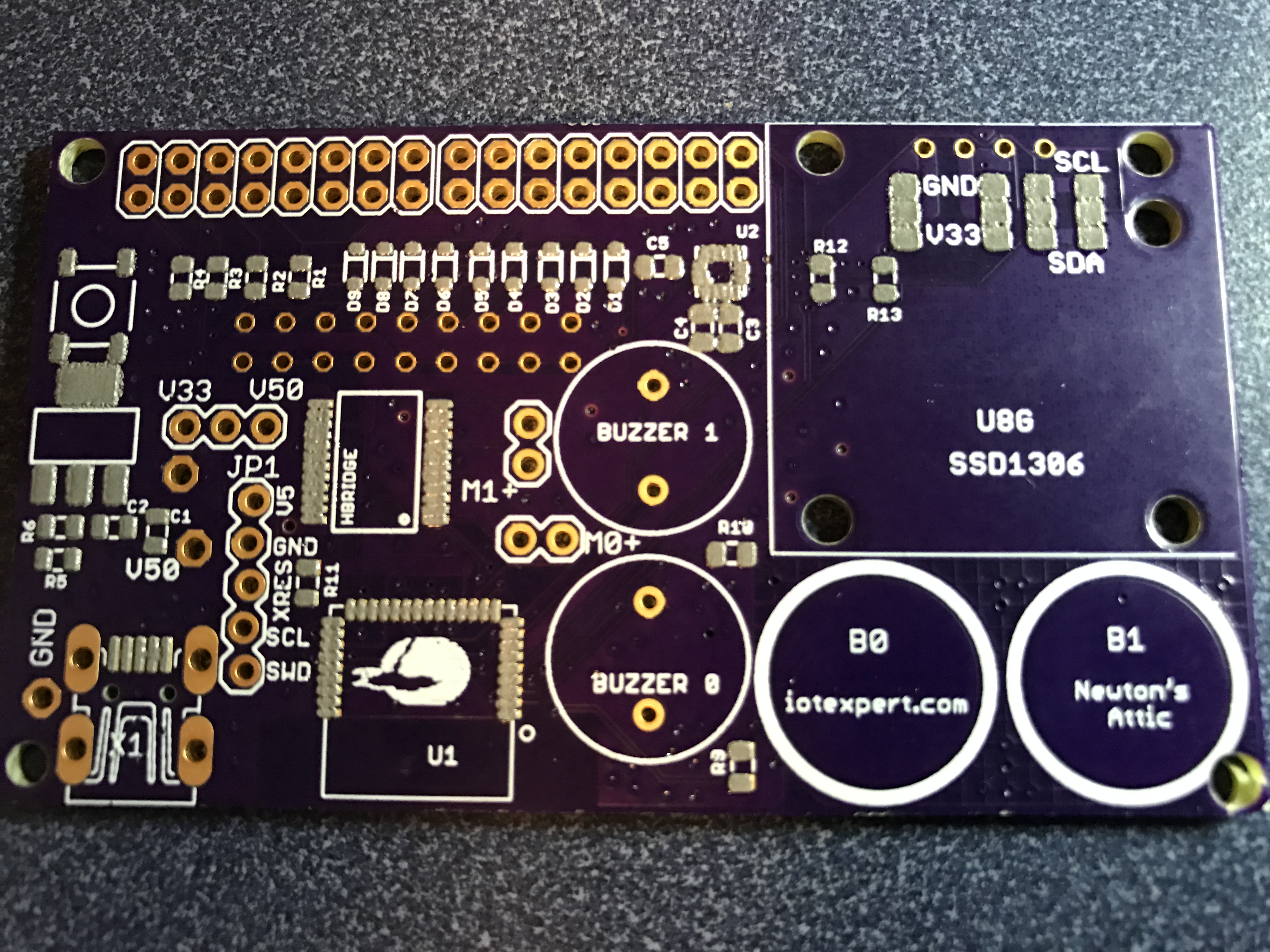
Once you have the solder paste screened onto the board, you should look at it carefully.  I typically use my microscope because my vision is not that great.  However, this blowup picture of the board works pretty well.  The only real problem in this picture is the blob of solder on U2 (the Accelerometer) which will cause problems in the reflow.  It is very tough to not get too much solder on the 0.5mm pitch pads.

Place all of the Parts onto the PCB

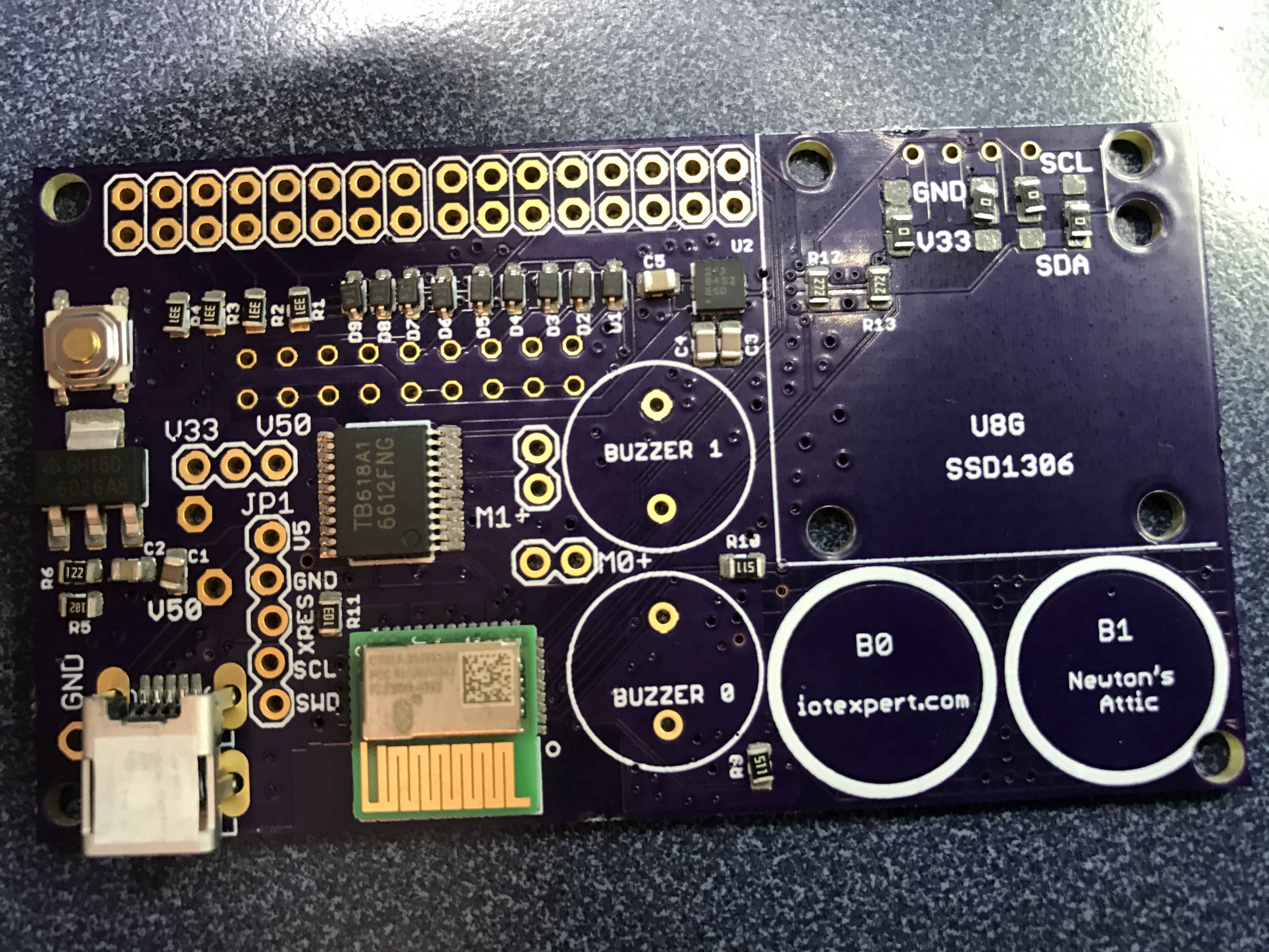
I was originally planning on making a video of placing the parts onto the board.  But, I need to look in the microscope while I am placing the parts on the board and I didn’t have a good way to record video.  I use a pair of Hakko 7-sa non-static tweezers  which I bought from Amazon.  I have a bunch of different pairs of tweezers and these are by far the best.  This is a picture after all of the parts are placed:

Place in Qinsi QS-5100 PCB Solder Reflow Oven

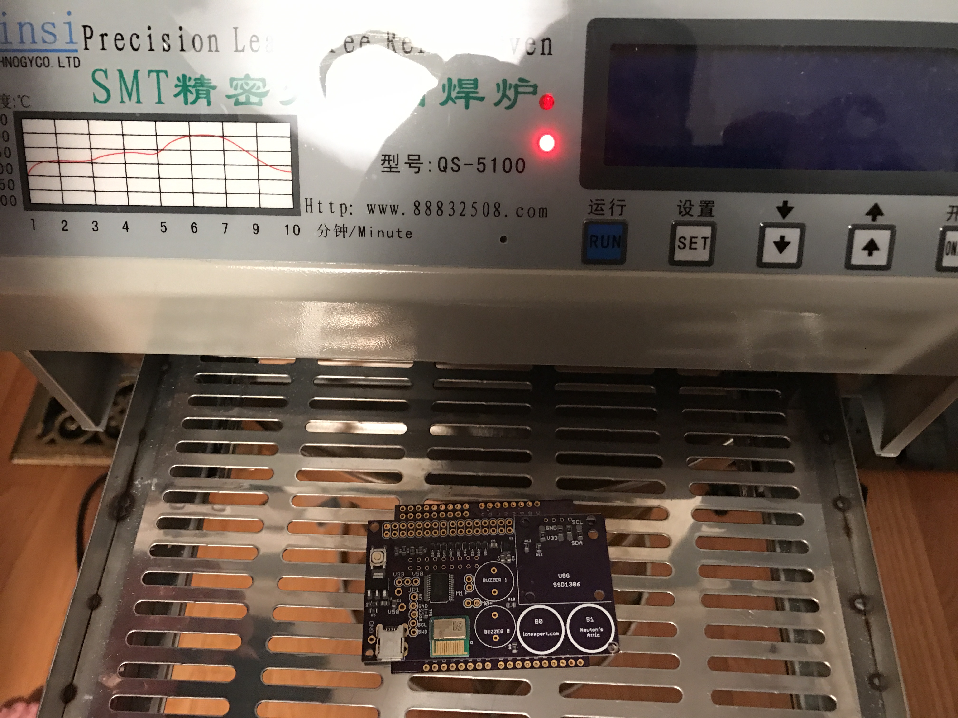
Now that you have the parts placed onto the PCB, it is time to place it in the PCB solder reflow oven.  I have found that it works best to have my PCB sitting on another board in the middle of the tray (a tip that I got from Ian Lesnet of Dangerous Prototypes).

Visually Inspect the Solder and Clean up any Solder Balls

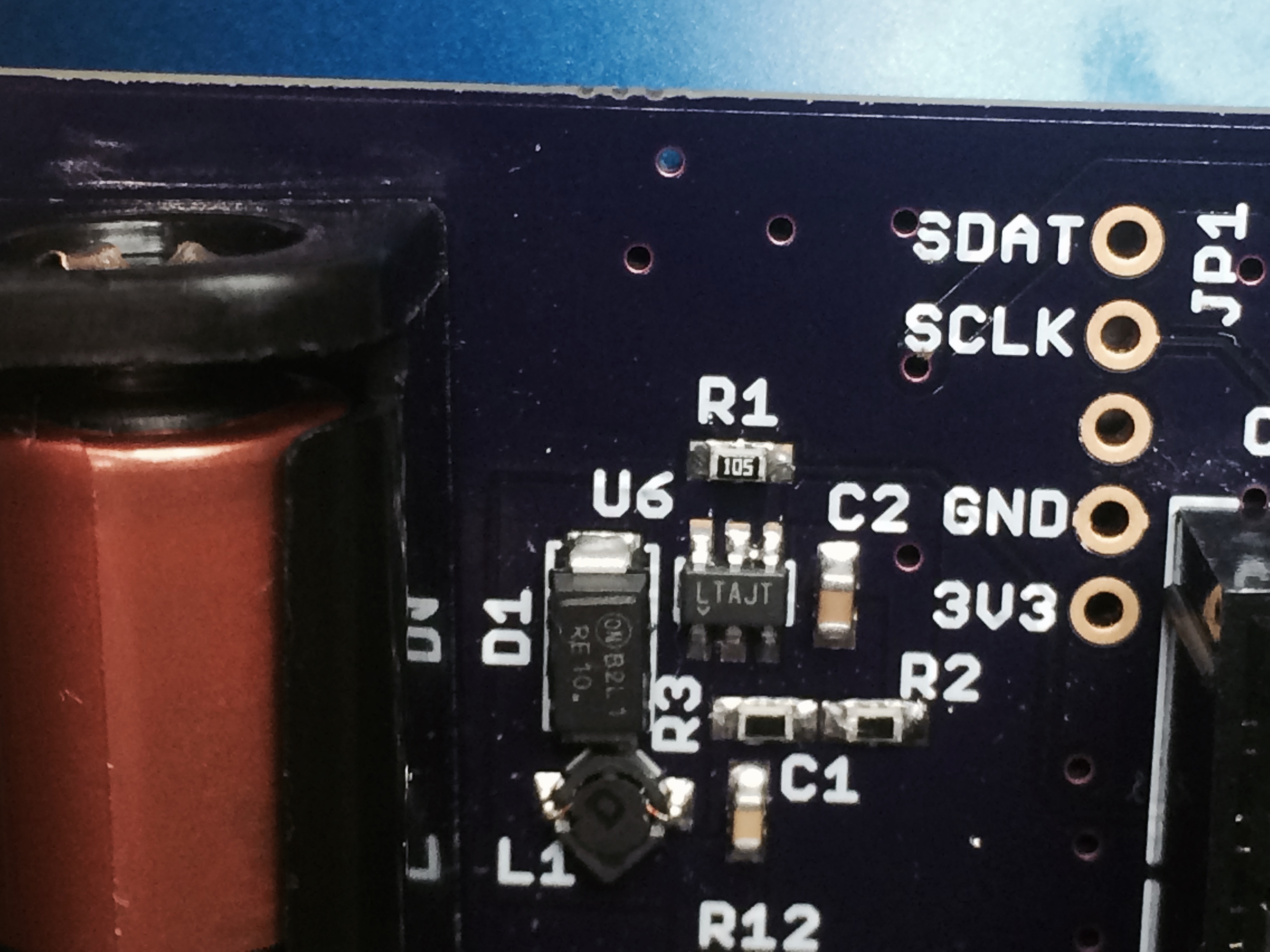
I almost always end up with 1 or 2 solder balls stuck between the pins of one of the chips.  When you are running the reflow, solder that isn’t attached to anything will ball up because of the surface tension.  Murphy’s law says that the solder balls will not end up anyplace good, and will for sure short some pins together.  You should look carefully for these balls or bridges and clean them up with your soldering iron.  This is a picture of a solder ball from another project.  You can see it between the right two pins on U6 (the chip labeled LTAJT).  The easy way to fix the ball is to squirt a little bit of flux on it, then touch it with your soldering iron.  That will melt the ball onto the pins next to it.

Solder the Programmer Connector into the PCB

The (almost) last step is to solder on the header for the Miniprog-3.  Then let it rip with a blank program program.

Cleanup the Disaster Area

Once all of that is done, my office is a complete and total disaster area.  Yes, I use gloves when I work with solder and you should as well.

In the next post I will take you through the steps I followed to test the Pinball PCB.

You can find all of the source code and files at the IOTEXPERT site on github.

Index Description
Pinball: Newton's Attic Pinball An introduction to the project and the goals
Pinball: Lotsa Blinking LEDs Everyone needs a bunch of LEDs on their Pinball Machine
Pinball: Matrix LEDs (Part 1) Saving PSoC pins by using a matrix scheme
Pinball: Matrix LEDs (Part 2) Solving some problems with the matrix
Pinball: Matrix LEDs Component How to turn the Matrix LED into a component
Pinball: A Switch Matrix Implementing a bunch of switches
Pinball: Switch Matrix Component (Part 1) The switch matrix component implementation
Pinball: Switch Matrix Component (Part 2) The firmware for matrix component
Pinball: Switch Matrix Component (Part 3) Test firmware for the matrix component
Pinball: The Music Player (Part 1) The schematic and symbol for a Music Player component
Pinball: The Music Player (Part 2) The Public API for the Music Player component
Pinball: The Music Player (Part 3) The firmware to make the sweet sweet music
Pinball: The Music Player (Part 4) The test program for the music player
Pinball: The Motors + HBridge Using an Bridge to control DC Motors
Pinball: The Eagle Schematic All of the circuits into an Eagle schematic
Pinball: The Printed Circuit Board 1.0 The first Eagle PCB layout of the printed circuit board
Pinball: The PCB Version 1.0 Fail Problems with the first version of the Eagle PCB layout
Pinball: PCB Layout 1.2 Updates using Eagle Fixing the errors on the first two versions of the Eagle PCB
Pinball: Assemble and Reflow the 1.2 PCB Assembling the Eagle PCB
Pinball: Testing the Eagle PCB Firmware to test the newly built Pinball printed circuit board
Pinball: Debugging the Motor Driver Fixing the motor driver PSoC project
Pinball: Hot-Air Reworking the Accelerometer Solder Using a Hot-Air Rework tool to reflow a QFN
Pinball: Debugging the LM317 Power Supply- A Tale of Getting Lucky Debugging the LM317/LM117 power supply
Errors in this Blog & A Tribute to Donald Knuth

Background for new Blog Error Policy

I have the writing background of a typical engineer.  That is to say, not very good.  However, in the last twenty years, I have come to believe that excellent writing skills are central to success as an engineer.  As such, I have put a lot of time and energy into improving mine,  sometimes with more success than others, as you have probably noticed.

In the name of improvement, I will make you this offer:  if you are the first to post a comment about an error in the blog, either in the writing or in the engineering, I will mail you a Cypress Development Kit.  This offer is effective for all posts starting January 1, 2017.  The only condition of this offer is that I am the sole and final arbiter of errors.

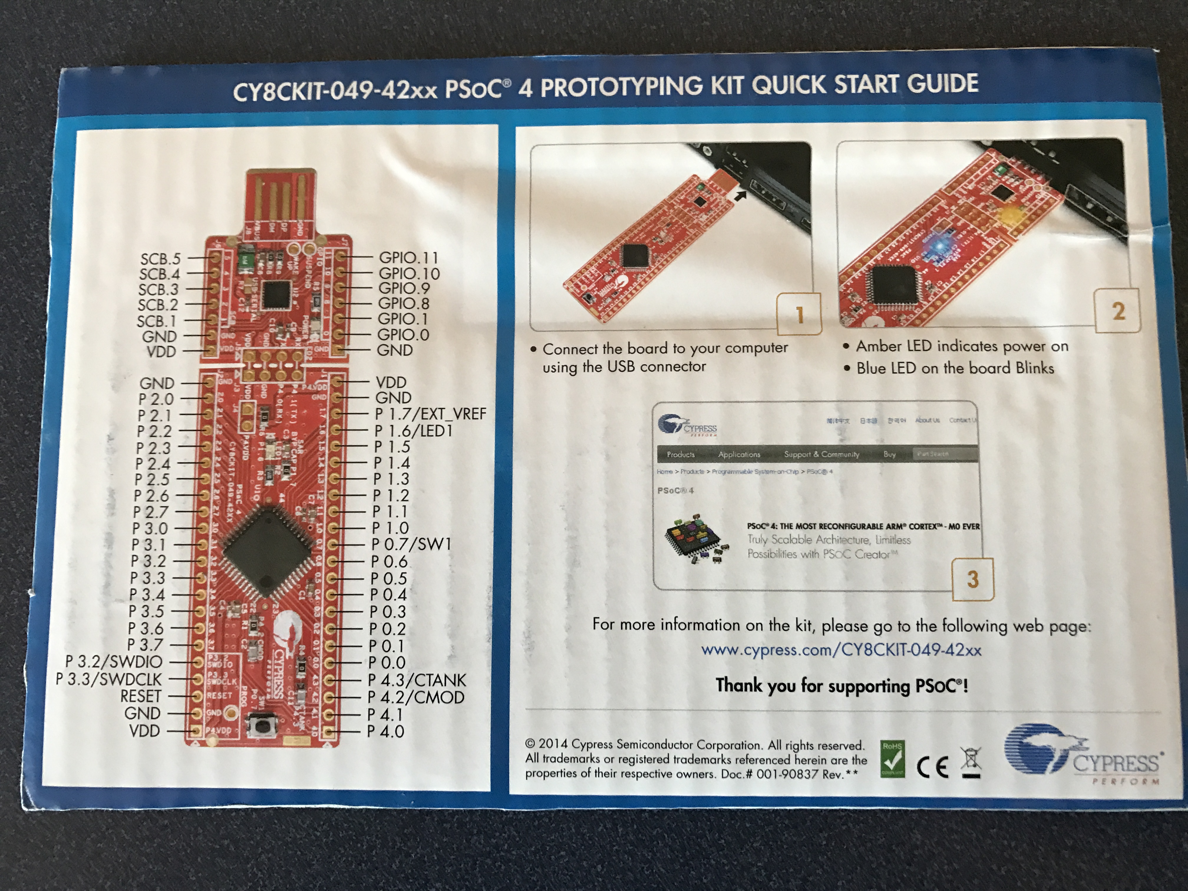
CY8CKIT-049

CY8CKIT-049

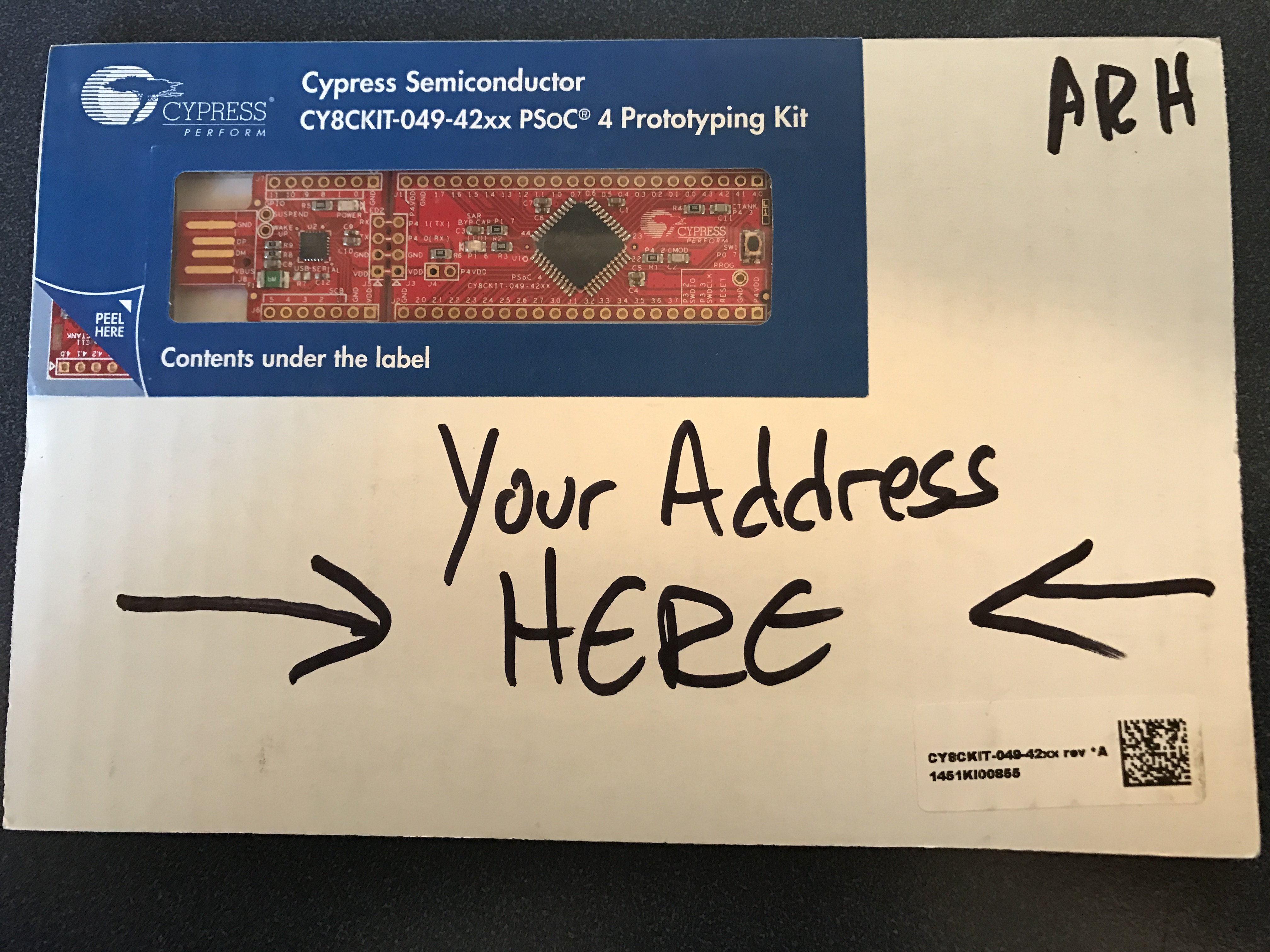
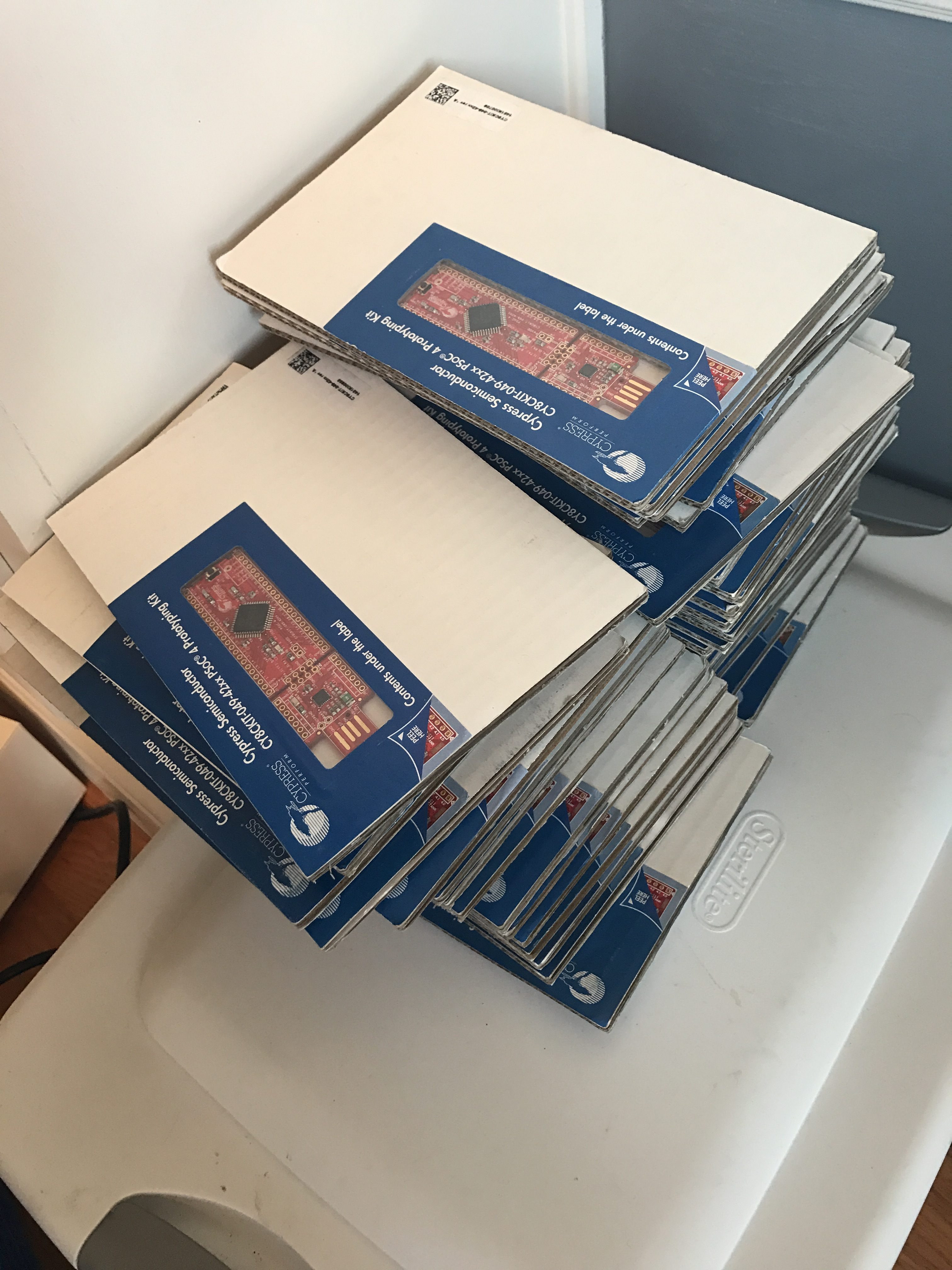
Here is a pile of the development kits in the corner of my office, ready to be sent out.  Hopefully, there won’t be too many. 🙂

A big stack of CY8CKIT-049 Ready to be Sent

The idea of offering a prize is hardly novel.  In fact, Donald Knuth has done the same thing for years.   You can read about it in the Wikipedia article Donald Knuth Reward Check.  In addition, there are many people who have posted pictures of their check.

Donald Knuth Prize Check

I hardly think that my writing is the calibre of Donald Knuth’s, but it will serve as good motivation to be careful.  I look forward to hearing from you.

Alan

Pinball: PCB Layout 1.2 Updates using Eagle

Goals for fixing the PCB Layout using Eagle

In the last Pinball post I talked about the 1.0 version of the Eagle PCB not working.  You might notice that the version number on this post is 1.2.  It seems strange to skip a version number.  Well, it turns out that I didn’t skip a version number in fact,  I did the most ridiculous thing possible, I made exactly the same error twice in a row on the PCB layout. That is, I flipped a chip footprint.  Enough about that.

In this post I am going to talk about the new printed circuit board.  As I updated the PCB design for this version of the board I had the following objectives

  1. Fix the flipped footprint
  2. Put a 1″ LCD screen on the board
  3. Move the whole system to 3.3v and simplify the power routing
  4. Provide a jumper selectable 5v/3.3v source for the motors
  5. Fix the USB footprint to a USB plug that can be purchased
  6. Make the silkscreen more readable (and fix the errors)
  7. Fix the ground plane grid on the CapSense Buttons

Here is the OSH park rendering of the new PCB layout.

OSH Park Rendering of Pinball 1.2 Eagle PCB Layout

Fix the flipped footprint

I would have bet money that I fixed the Eagle library to have the correct foot print when I did PCB 1.1.  However, after I renumbered the pins in the package editor, I did not unhook and then rehook them in the library editor.  The result was a flipped footprint, again.  What is particularly frustrating is that I didn’t recheck it on the PCB.  I now have added that to my PCB checklist.

Put a 1″ LCD screen on the board

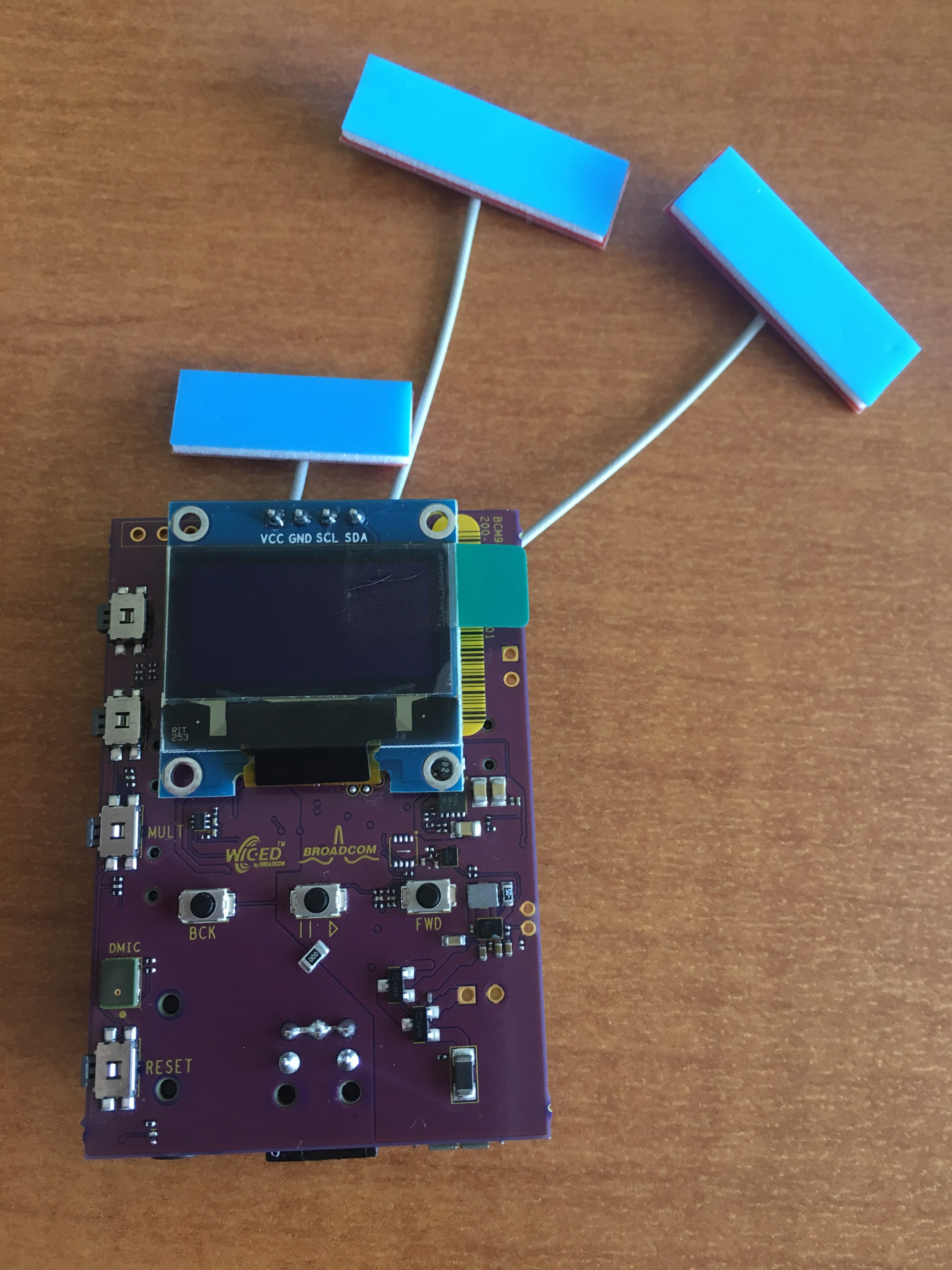
On one of our WICED WiFi development kits, the IoT team put a really cool 1″ OLED LCD screen.

Internal WICED 943907 WiFi Development Kit with OLED Screen

After I looked around a little bit, I found that the little screen was very available for $3-ish on eBay.  My original plan was to use a bigger screen with an external connector.  But these aren’t as cool and they cost $8.  See what I am saying?

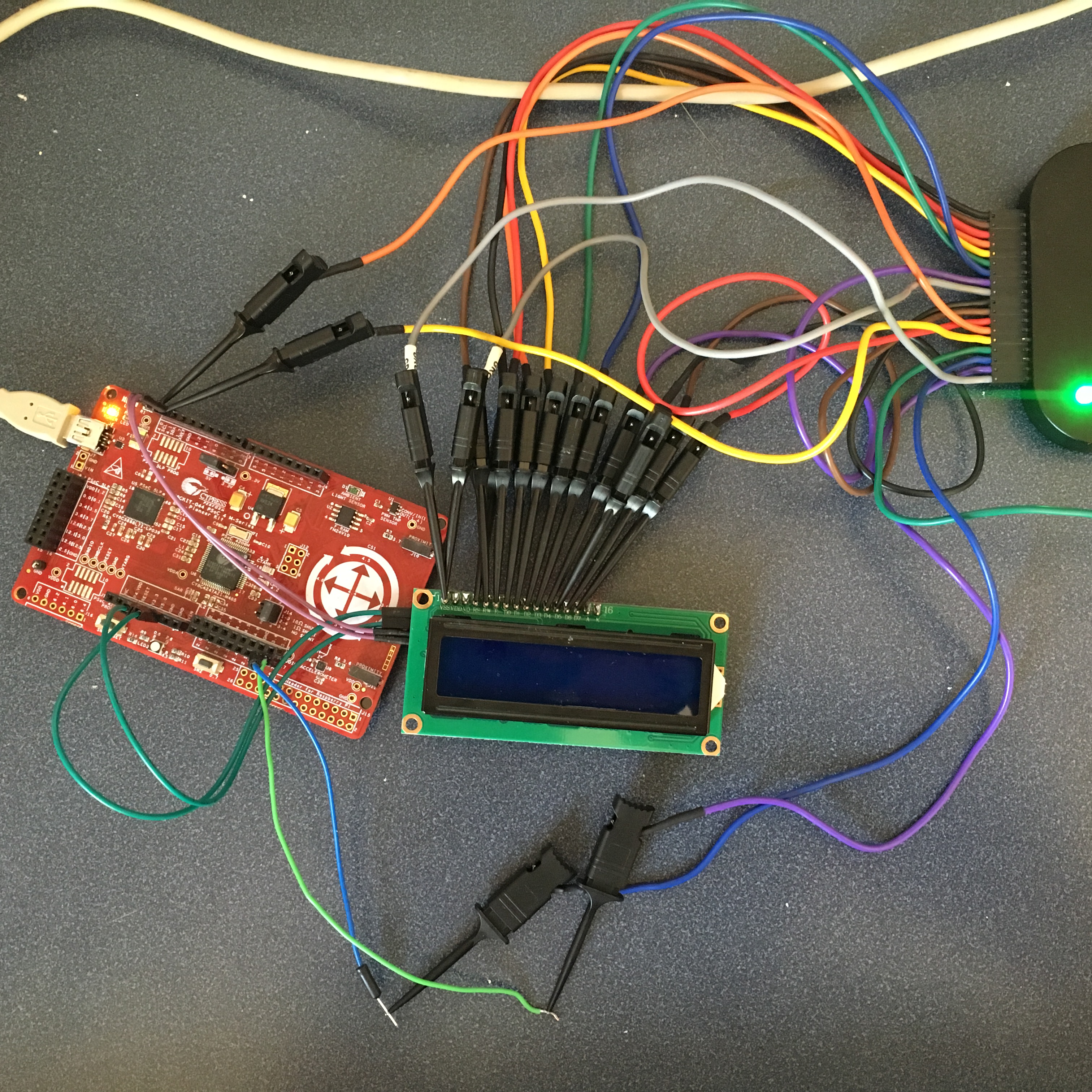
16x2 Hitachi LCD Screen with PSoC 4200M Development Kit

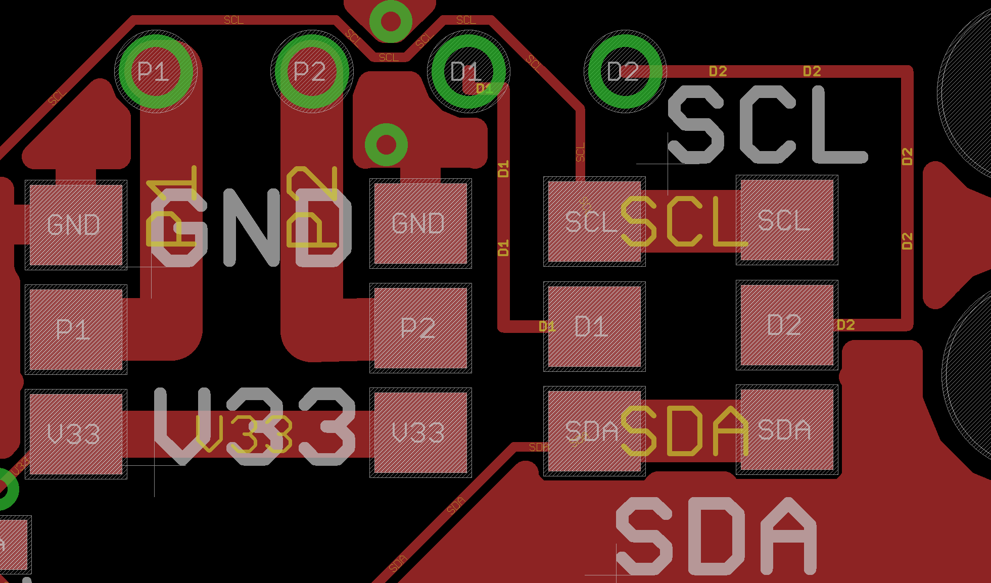
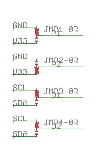
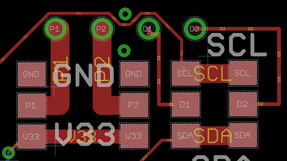
In the upper right hand part of the PCB, I extended it a little bit and put on the footprint.  The only hitch is that it appears sometimes the pins are “VCC/GND” and sometimes the pins are “GND/VCC”.  In order to handle this, I setup four 0-Ohm resistors to allow me to switch the pins.

PCB Layout with 0 Ohm Resistors to select SDA/SCL and GND/VCC

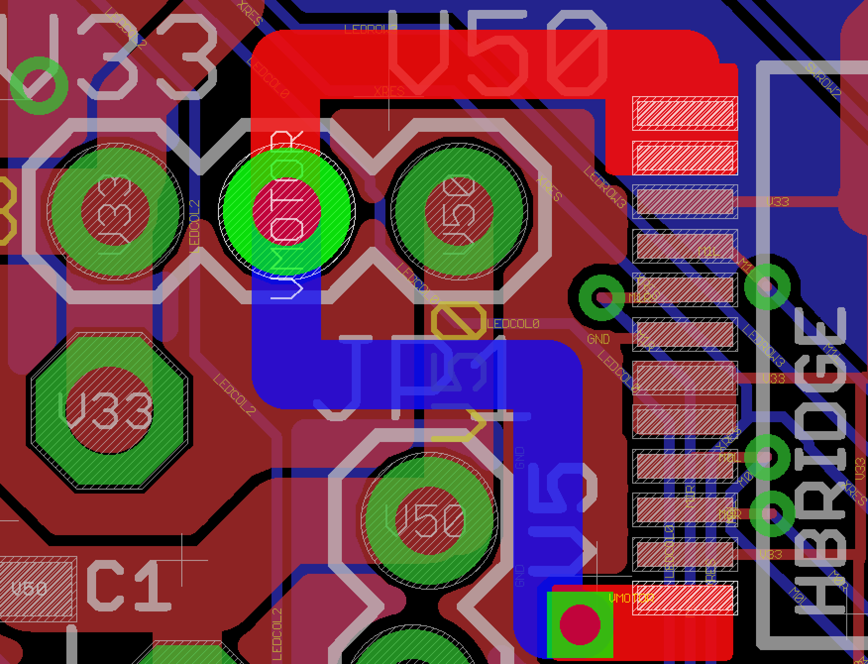
Move the whole system to 3.3v and simplify the power routing

There was no reason to run the system on 5V other than giving a little bit of extra power to the motors.  So, to simplify things I moved the PSoC to 3.3V (which it will happily do).  That allowed me to remove the level translator that I was using for the accelerometer.  By doing this, I could move all of the 5V power to the far left of the PCB, and not route it all over the place.  Here is a screen shot of the PCB layout.  You can see that the power comes in from the USB connector, then goes straight to three places

  1. The 3.3v Regulator
  2. The Mini-Prog-3 Connector
  3. The Motor Power Selector

Eagle PCB layout of 5.0v power supply

Provide a programmable 5v source for the motors

I setup the motor power to be either 3.3v or 5.0v based on the selection of a jumper.  The jumper is a 3-position header on 100 mil spacing.

Eagle PCB layout of motor power supply selection jumper

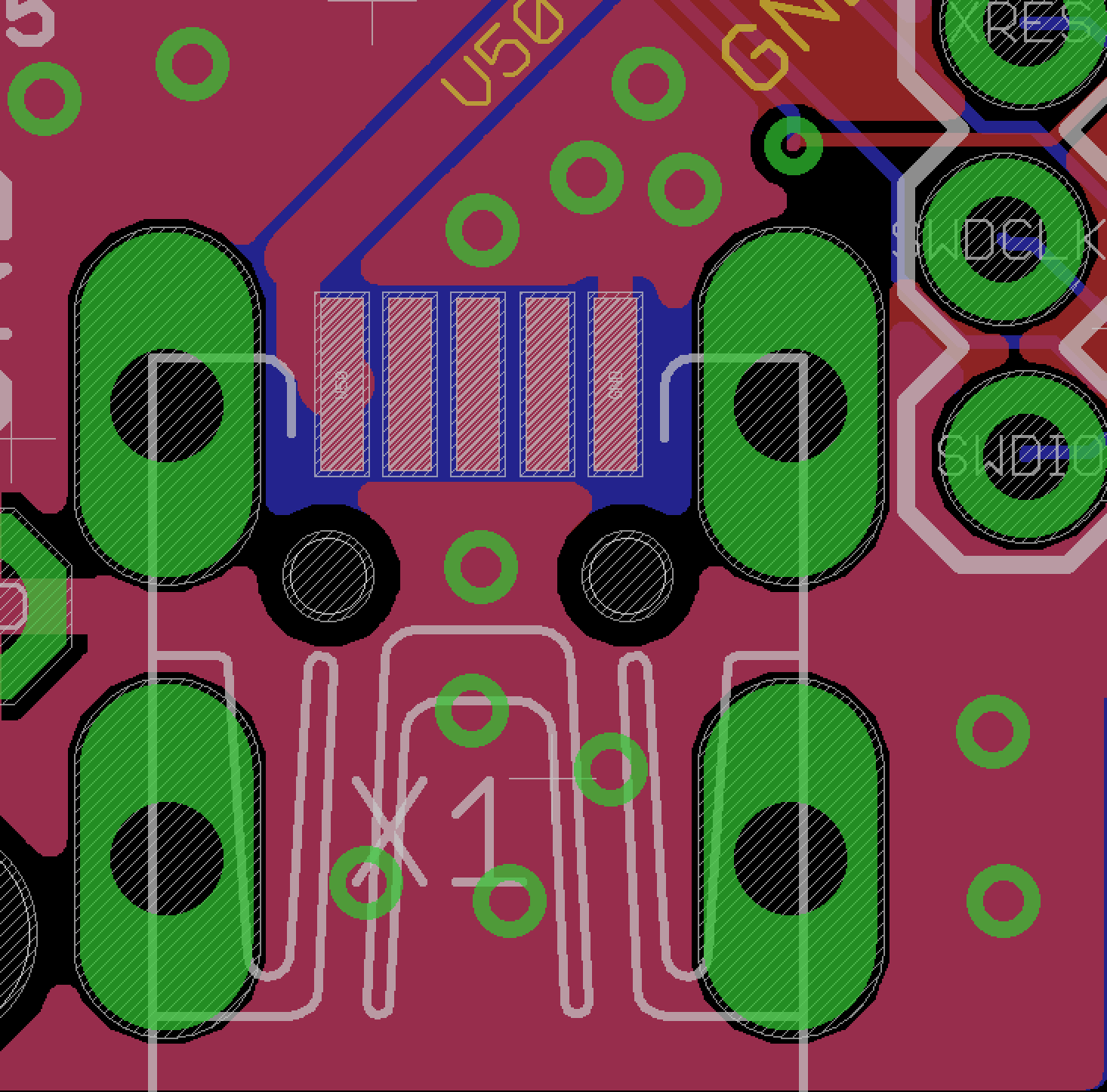
Fix the USB footprint to a USB plug that can be purchased

In the first version of the Pinball PCB layout I used a USB footprint that I found on the internet.  But, it turns out that footprint was not available.  In fact, I had to search and search for those parts.  I finally found a scrap shop in Poland that had a few of them available.  That was a bad idea.  Here is the new footprint:

Eagle PCB layout footprint of USB connector

Make the silkscreen more readable (and fix the errors)

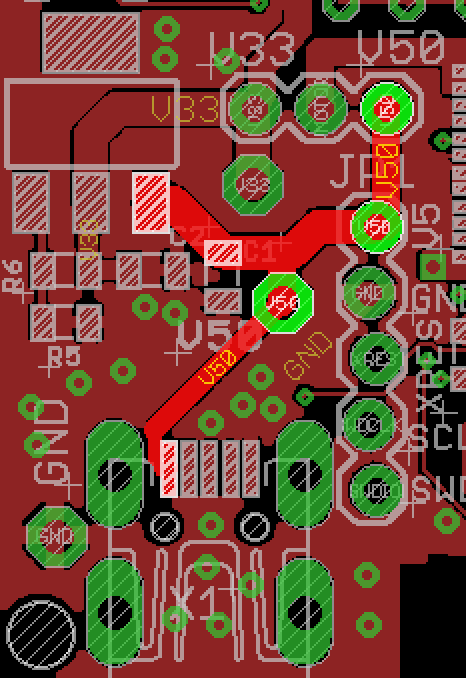
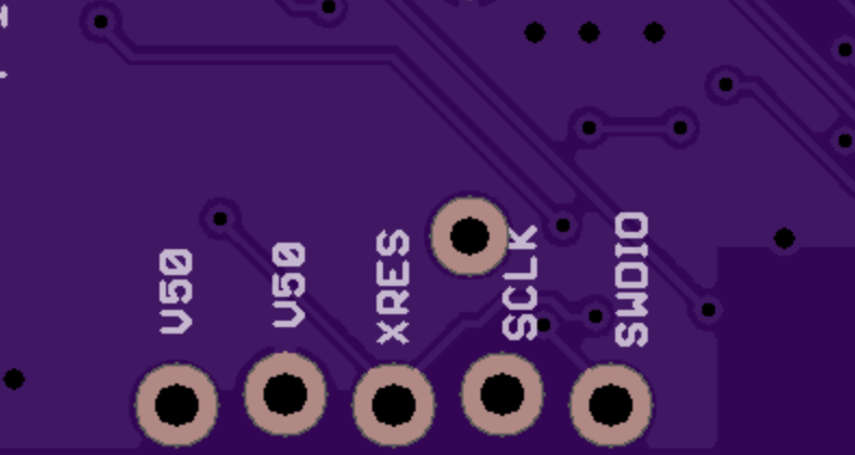
My eyes really don’t like any silkscreen that is less than 30mils tall.   There are some people who can see a smaller font, but I am just not one of them.  I really prefer 40mil tall letters to occur in my PCB layout.  I have updated the checklist with a chart of what is legible and illegible.  In addition I had a few errors like the one below (there aren’t two V50 pins next to each other, one is supposed to be ground.)

silkscreen error in original PCB layout

Fix the ground plane grid on the CapSense Buttons

To get the best CapSense performance you should not use a solid ground plane in your PCB layout (like the one below).  You should use a cross hatched ground (like the picture at the bottom).  You can read about this in the Cypress application note or in my design guidelines.

solid ground pour around PSoC Capsense PCB layout

Cross hatched ground pour around Cypress PSoC Capsense PCB layout

You can find all of the source code and files at the IOTEXPERT site on github.

Index Description
Pinball: Newton's Attic Pinball An introduction to the project and the goals
Pinball: Lotsa Blinking LEDs Everyone needs a bunch of LEDs on their Pinball Machine
Pinball: Matrix LEDs (Part 1) Saving PSoC pins by using a matrix scheme
Pinball: Matrix LEDs (Part 2) Solving some problems with the matrix
Pinball: Matrix LEDs Component How to turn the Matrix LED into a component
Pinball: A Switch Matrix Implementing a bunch of switches
Pinball: Switch Matrix Component (Part 1) The switch matrix component implementation
Pinball: Switch Matrix Component (Part 2) The firmware for matrix component
Pinball: Switch Matrix Component (Part 3) Test firmware for the matrix component
Pinball: The Music Player (Part 1) The schematic and symbol for a Music Player component
Pinball: The Music Player (Part 2) The Public API for the Music Player component
Pinball: The Music Player (Part 3) The firmware to make the sweet sweet music
Pinball: The Music Player (Part 4) The test program for the music player
Pinball: The Motors + HBridge Using an Bridge to control DC Motors
Pinball: The Eagle Schematic All of the circuits into an Eagle schematic
Pinball: The Printed Circuit Board 1.0 The first Eagle PCB layout of the printed circuit board
Pinball: The PCB Version 1.0 Fail Problems with the first version of the Eagle PCB layout
Pinball: PCB Layout 1.2 Updates using Eagle Fixing the errors on the first two versions of the Eagle PCB
Pinball: Assemble and Reflow the 1.2 PCB Assembling the Eagle PCB
Pinball: Testing the Eagle PCB Firmware to test the newly built Pinball printed circuit board
Pinball: Debugging the Motor Driver Fixing the motor driver PSoC project
Pinball: Hot-Air Reworking the Accelerometer Solder Using a Hot-Air Rework tool to reflow a QFN
Pinball: Debugging the LM317 Power Supply- A Tale of Getting Lucky Debugging the LM317/LM117 power supply
IOT Expert 2016 Year in Review and 2017 Goals

Summary

This week as I looked back on 2016, I decided to evaluate where I have been with my project www.iotexpert.com and what the future should look like.

I started this website in the fall of 2014 when I was on vacation from Cypress.  In that first 4 months I made 14 posts, which, at the time, I thought was an OK start even though my original goal was to post 2x per week.  On December 7, 2014 I went back to work full time at Cypress and I let things get out of control in my personal life.  One signal of that problem was only two posts during 2015.  At the end of January 2016, I decided that my only goal for this site would be to post once per week for the  rest of the year.  I far exceeded that goal by completing 76 posts.  During 2016, I also started the @askiotexpert twitter feed as well as becoming the first or second google hit for “iot expert” and “iotexpert”.  In terms of opportunity for my website, the best thing to happen was the acquisition of the Broadcomm IoT group by Cypress.  This gave me easy access to WiFi, Bluetooth and Zigbee.  All three of these technologies will play a big role in the coming year.
All-in-all I am pretty happy with the results. But, I think that I have learned quite a bit that will improve your experience for the future.

2016 Data

Topic # Posts Comment
The Creek 21 IOT-ifying the Elkhorn Creek with PSoC
Pinball 19 PSoC component projects, board design etc for the non-profit Newton's Attic
PSoC 4000s 11 Smart IO, BLE and CapSense projects for the PSoC 4000s series
CY8CKIT021 8 A bunch of PSoC projects for the new teaching development kit
Electronica 2016 5 Building up demo projects for Electronica
Personal Cloud Services 4 GIT,MQTT,AMQP,MAC Server, etc.
Maker Faire 3 My experience in Rome,New York, and the Bay Area Maker Faire's
WICED 2 The beginnings of a new series on IoT using Cypress WICED WiFi
Embedded World 1 My presentation from Embedded World
Eagle PCB 1 The most popular post of the year with rules for designing PCBs
Qinsi 1 The second most popular post of the year with temperature profiles from my Qinsi QS-5100 reflow oven

I made good progress with the number of page views and unique users through the year.  Though, it is clear that something happened in September and October that I should look at.

2016 Areas for Improvement

There are three areas that I feel that I should improve on for next year.

  1. Gaps in posts:  There were a couple of stretches where there was a multi-week gap between posts.  I need to make sure and work ahead so that I always have material on the hook to fill in the gaps that occur because of my travel.
  2. Quality:  I need to be continuously vigilant about my writing, grammar, spelling etc.
  3. Searching:  In order to make things easier to find by onsite and offsite (google) search I need to be very deliberate about using titles, tags and meta data.

2017 Goals

For 2017 my goals fall into three broad categories.  First, I want to continue creating (hopefully) interesting, high-quality IOT engineering content.  To that end I would like to:

  1. Achieve 2x/week posts and hit 104 posts for the year.
  2. Create a new video series and post 12 videos.

In addition to the new content, I would like to improve the accessibility of my website by

  1. Deploying a mailing list
  2. Automatically connecting to Twitter
  3. Automatically connecting to Facebook
  4. Developing a Linked-In strategy
  5. Fixing my release process to use best practices for all meta-data

such that I achieve

  1. 10x User Traffic
  2. 10x Twitter followers on @askiotexpert
  3. 10 Google keywords where www.iotexpert.com is a first page hit

Lastly, I want to update and deploy a new brand for iotexpert including logo’s, web page headers, Facebook covers, etc.

This year should be interesting.

Alan

Pinball: OLED Display

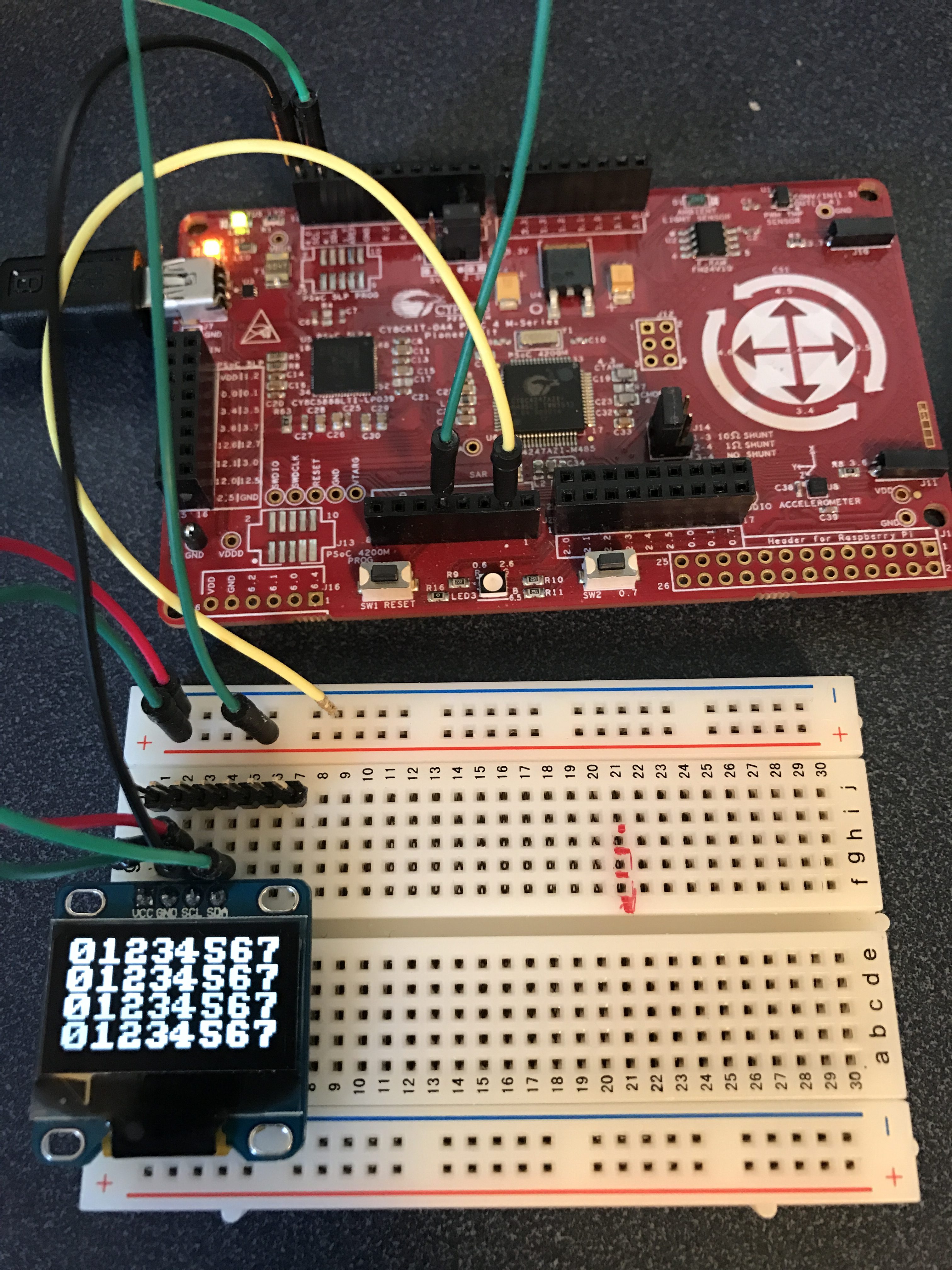
I screwed up the Pinball board design AGAIN!!!  It is so frustrating.  Ill write about the new design soon (and punish myself for the error.) As I worked on redoing the design I decided to put a footprint on the PCB for a small OLED LCD.   The display has an I2C interface, is about an inch wide and has 128×64 pixels… But, best of all can be purchased on eBay from China for about $3.00.  Here is a picture of the display with a PSoC4M driving it:

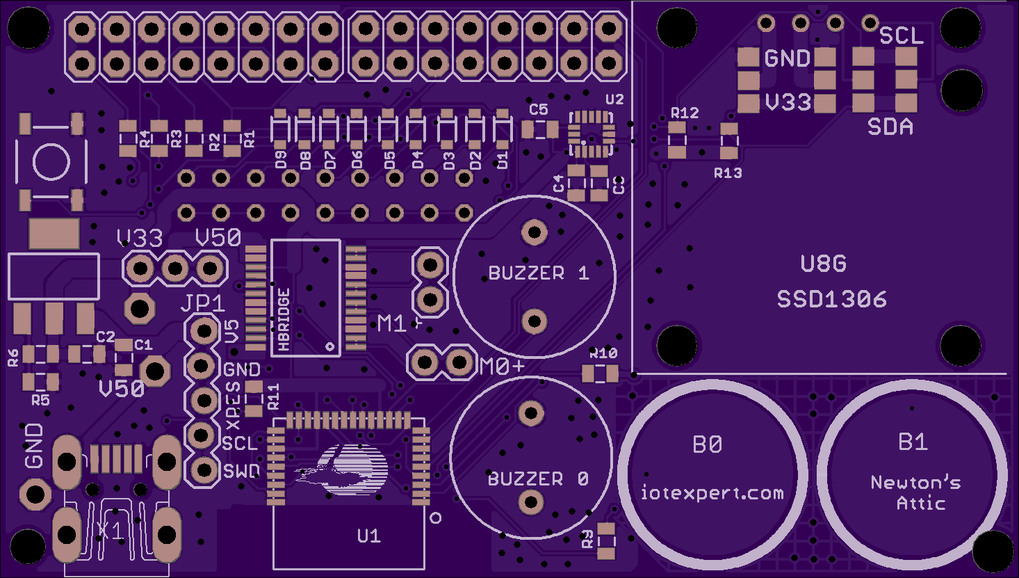
The display will go on the right side of the board.  Here is a rendering of the new board from the OSH Parks website:

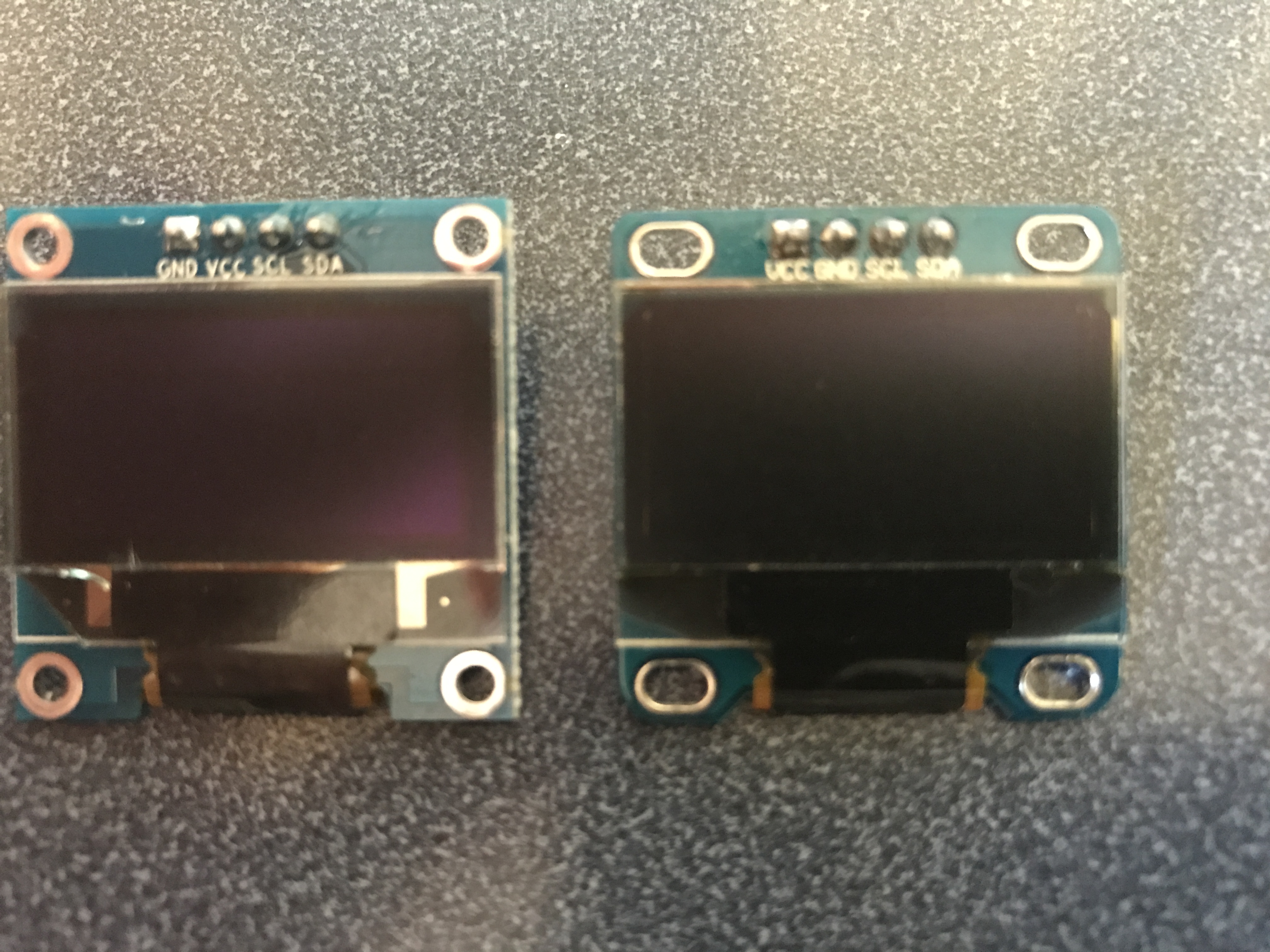
After I decided to put the footprint on the board I bought several displays from Amazon to try out, and to make sure that I knew how to make them work.  I immediately ran into some drama which caused me an evening of frustration.  If you look at the picture closely you can see that the power and ground pins are swapped:

After I realized that was going to be a potential problem I put in a set of 0 ohm resistors on the upper right hand part of the board so that I could swap power/ground and scl/sda connections.  Here is a snapshot of the schematic and layout:

This left me with what software to use to drive the display which I will address in the next post.


Qinsi-QS5100 Sn63Pb37 Solder Profile

About 2 years ago, I bought a Qinsi QS5100 reflow oven from China via Amazon.com.  My decision was based almost completely on the nice youtube video that Ian Lesnet from Dangerous Prototypes posted about his results.  After I got the oven, I successfully built a series of Physics Lab boards with it.  Then one day about a year ago, I got two boards in a row with horrible results which I attributed to the temperature profile.  A few weeks later, I dug around on the internet and decided to change to the Lesnet profile and things seemed to be working again.

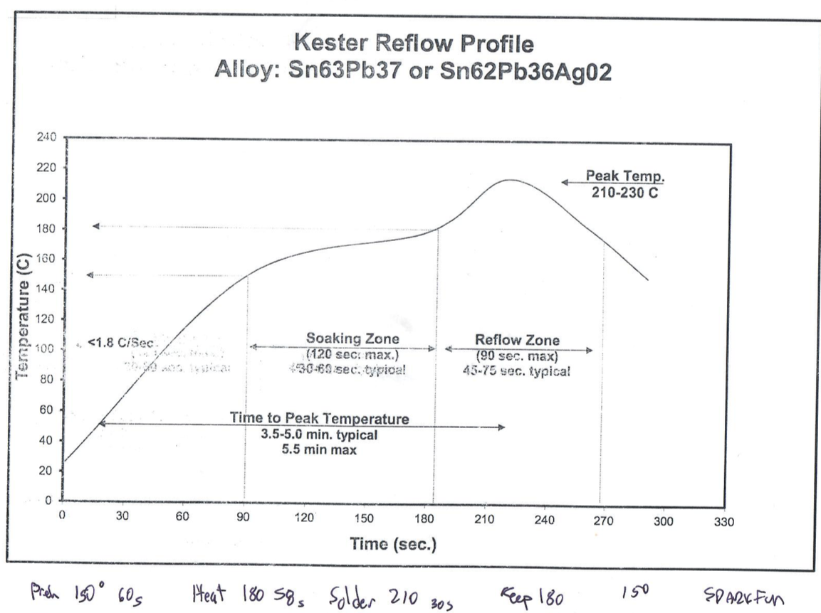
I have always had this bouncing around in the back of my head as a potential problem because I wasn’t SURE about the source of my original problem.  And, I don’t really believe in magic, but I didn’t have time to pursue a root cause.  As I have had a little bit of time the last few days, I decided to dig in.  First, I found the data sheet for the Kester solder paste that I have been using.  Here is scan of the printout of a blown up section from the datasheet with my handwritten notes from the Lesnet video (which I incorrectly denote as Sparkfun)

screen-shot-2016-11-27-at-8-41-17-am

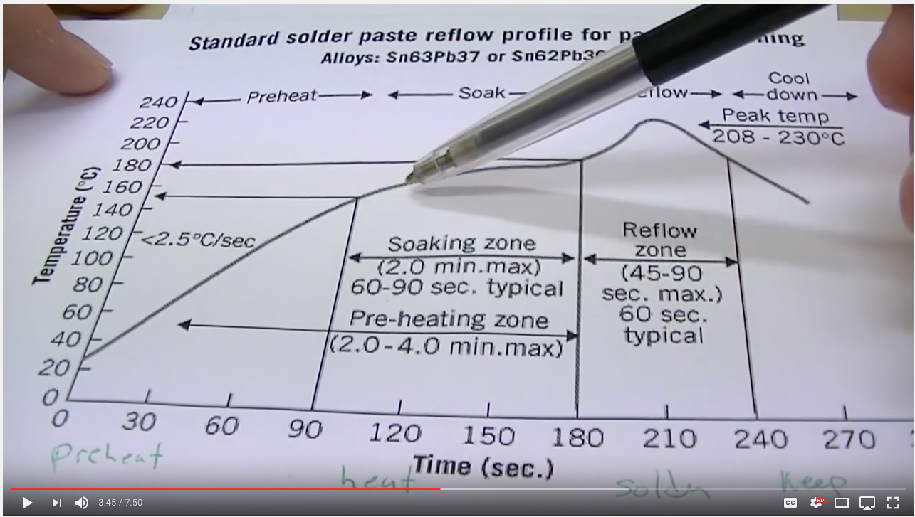
In fact in the video Mr. Lesnet shows a screenshot of a solder profile which is similar to the Kester data sheet.  I wondered why he didnt use that profile?

screen-shot-2016-11-27-at-8-57-22-am

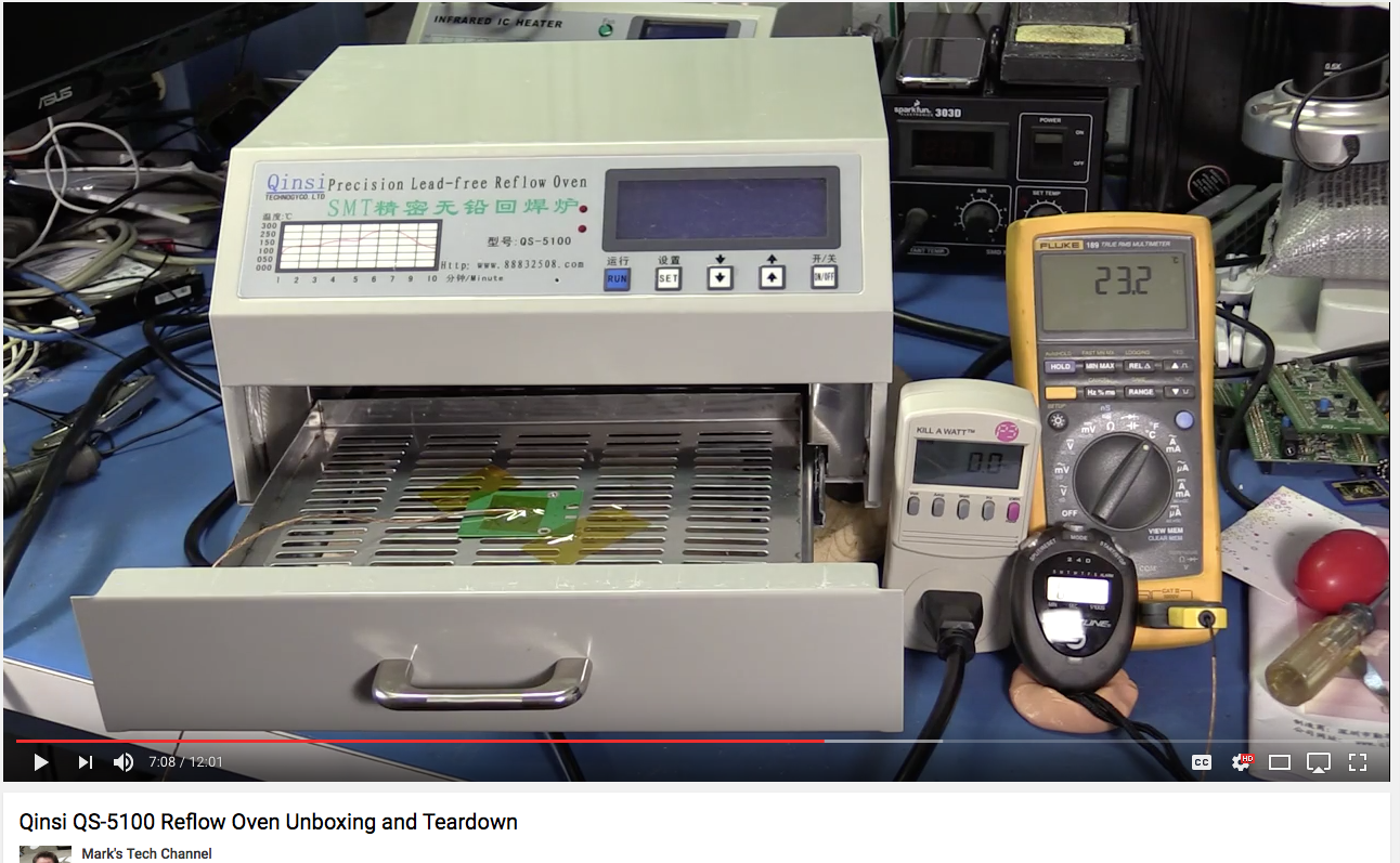
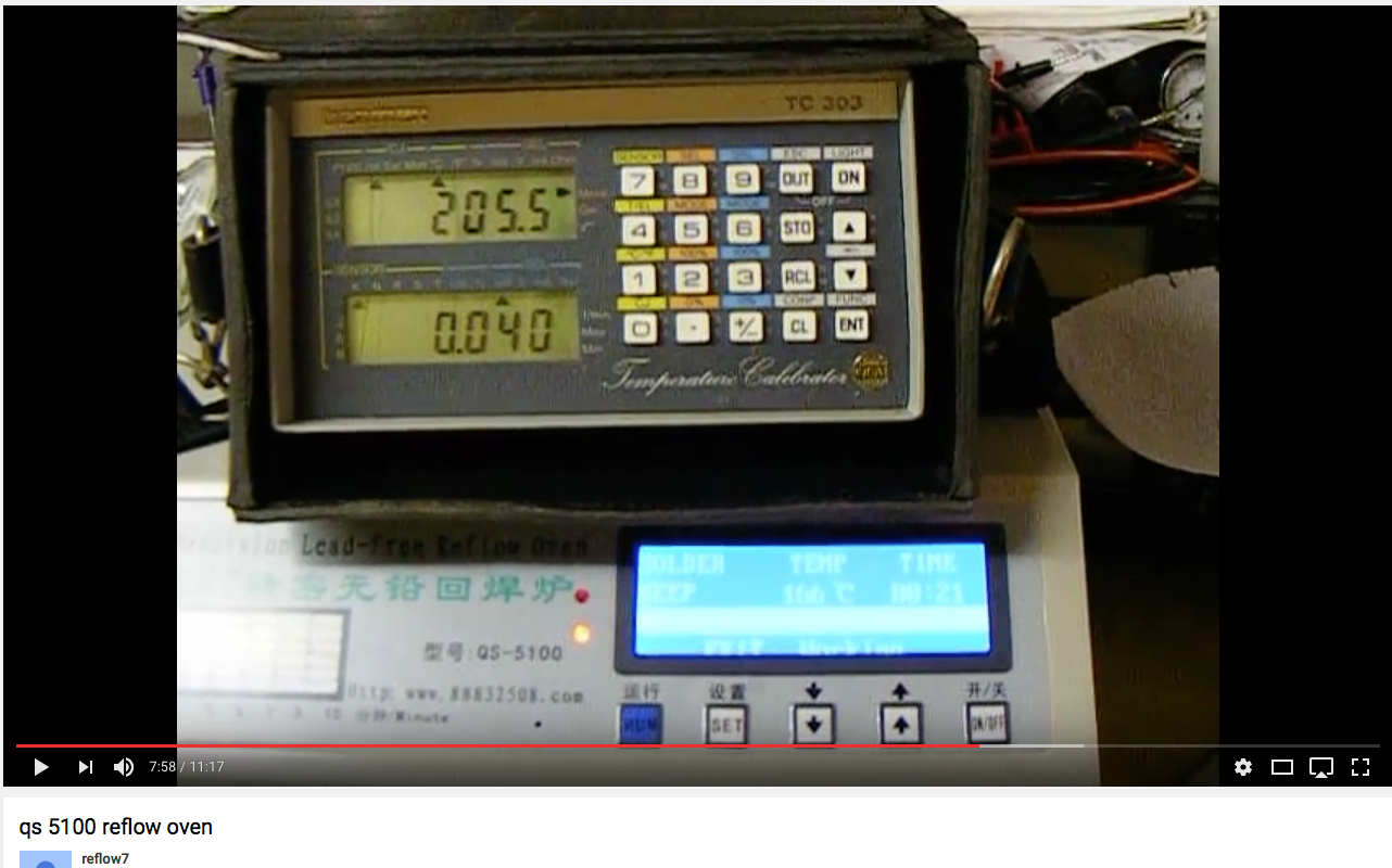
I had switched to using the Lesnet profile and was having consistently good results.  However, yesterday I decided that I wanted to compare that program with reality.  I found at least a couple of places on the internet where a comparison of the actual temperature and the programmed temperature were made with a Fluke & Thermocouple.

screen-shot-2016-11-27-at-9-00-03-amscreen-shot-2016-11-27-at-9-01-36-am

In the past I used the Fluke/Thermocouple method as well, but I found it difficult to compare a time based profile with instantaneous readings from the Fluke.  Moreover the numbers that you can read from the Kester data sheet don’t seem to match what you can enter into the QS-5100.  So, what in the world is the oven doing?

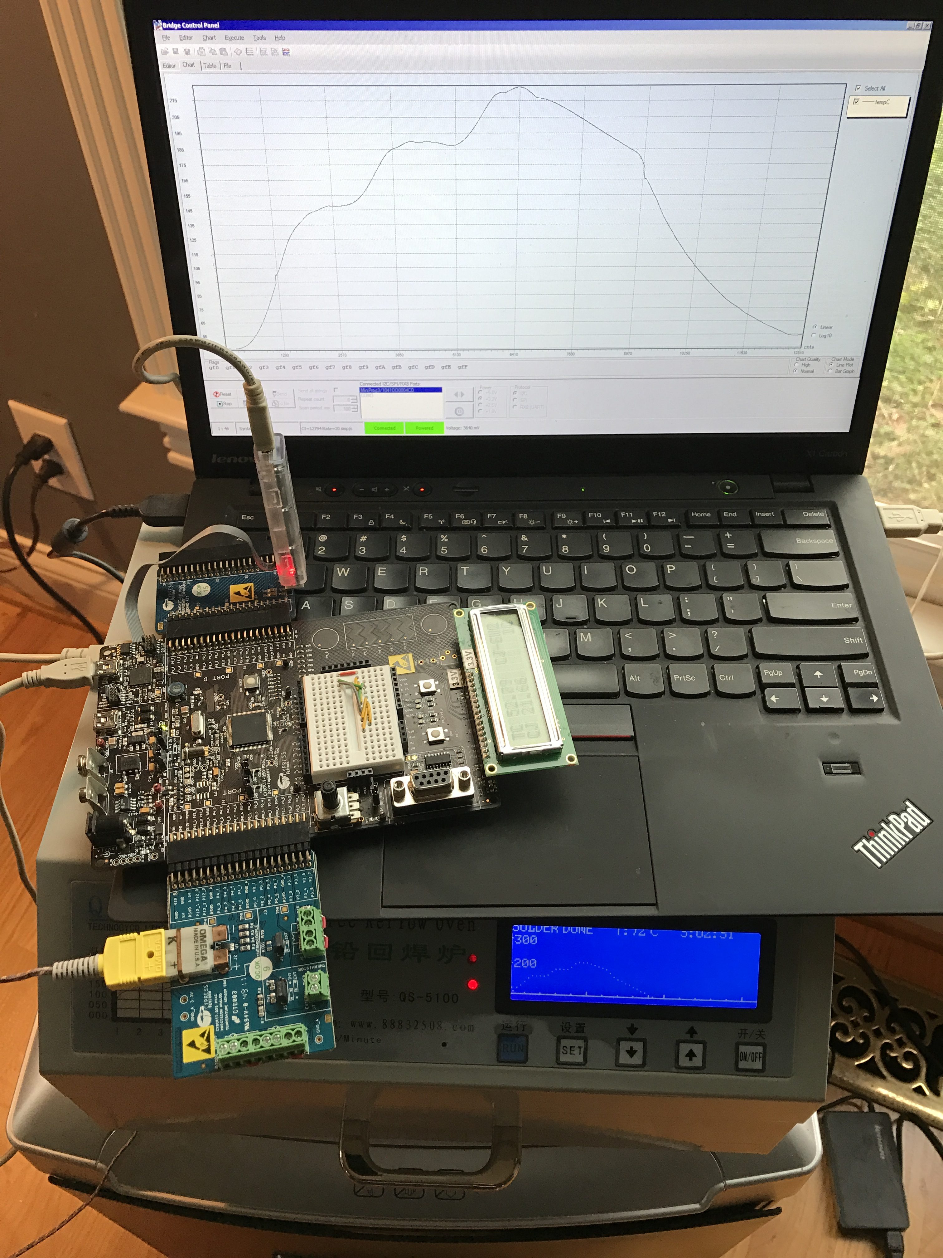
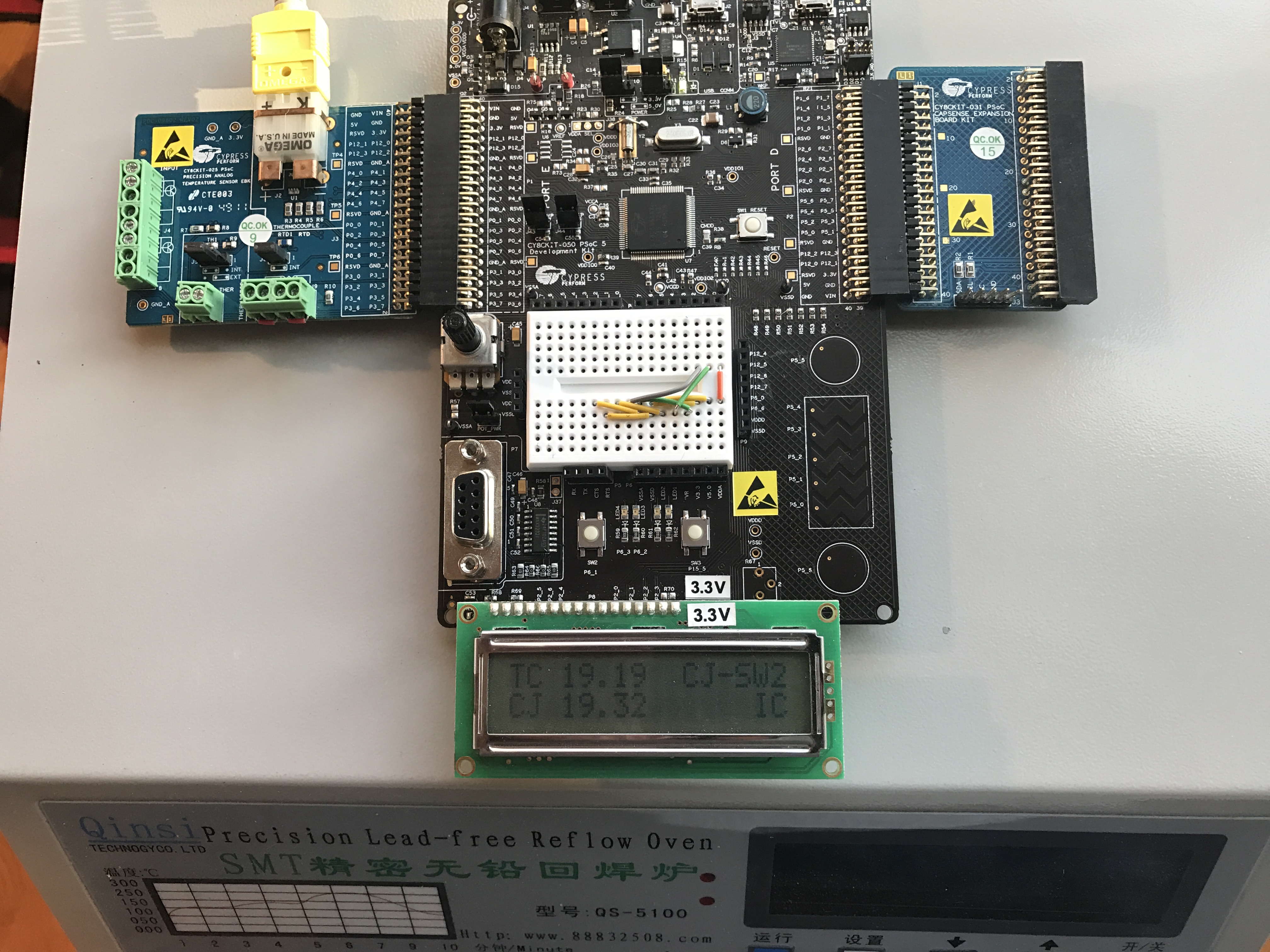
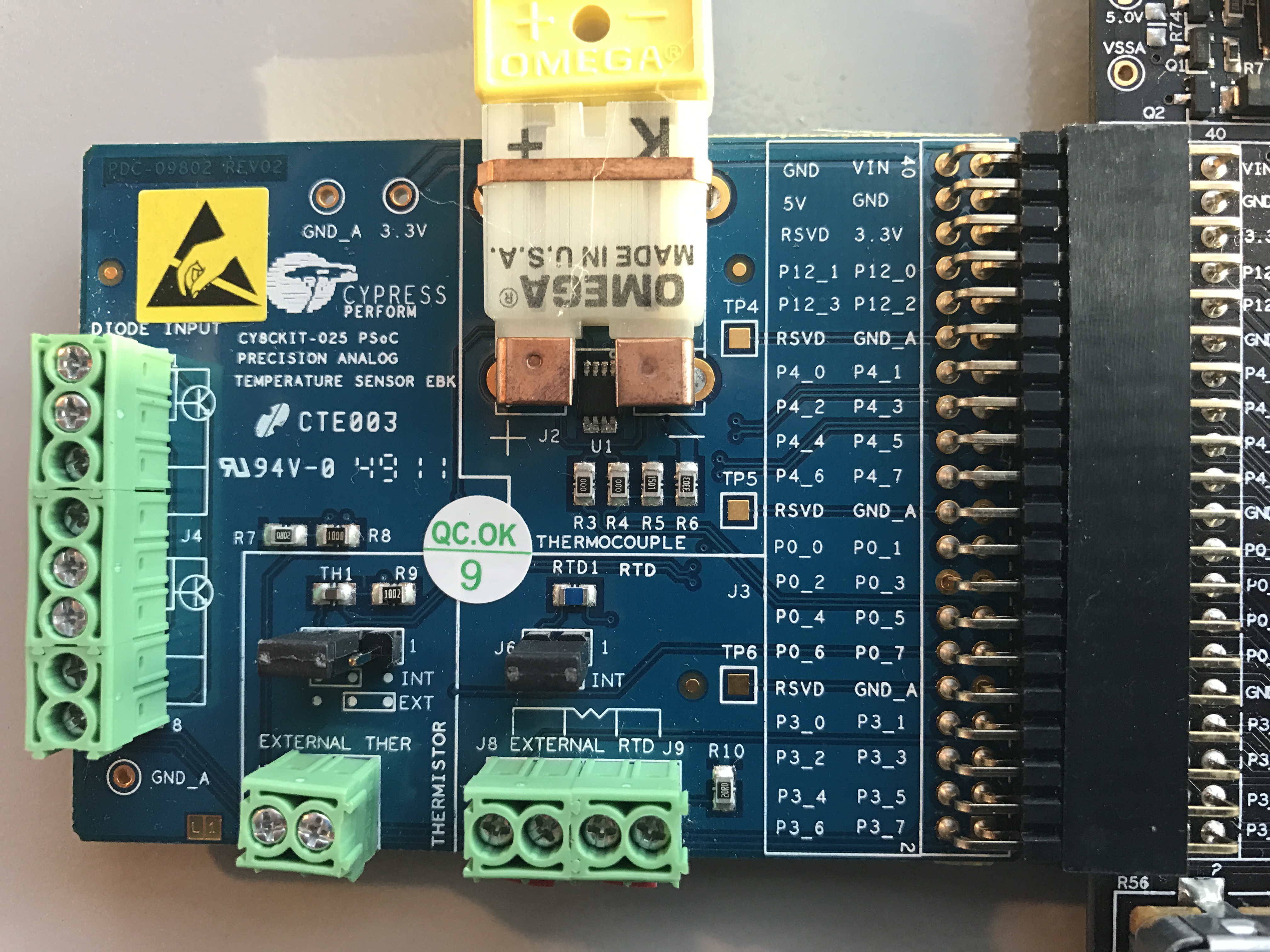
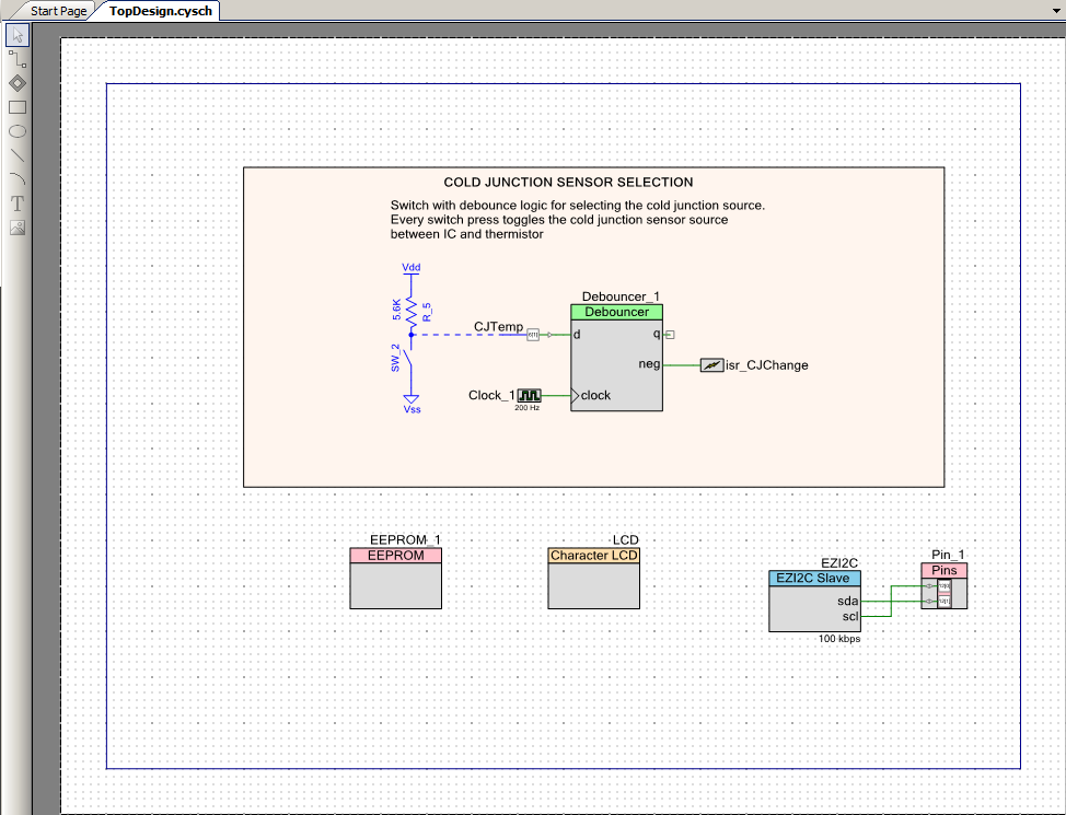
What I really wanted was to capture the data in realtime so that I could plot and analyze what the oven was doing.  To do this I used CY8CKIT-025 Precision Temperature Sensor Expansion Board attached to a PSoC5LP CY8CKIT-050 connected to the Bridge Control Panel to capture the actual PCB temperature into an excel file.  The CY8CKIT-025 has a K-Type thermocouple, a DS600 for cold junction compensation, a thermistor, an RTD and a temperature diode.  When paired with the 20-bit ADC in the PSoC5LP you are able to demonstrate a bunch of different methods for measuring temperature.  I used the example project that came with the kit with one modification, the addition of an “EZI2C”.   By putting in an EZI2C I was able to use the Bridge Control Panel to measure the temperature every 100ms and record that data to a file for analysis.  Here are several pictures of the setup:

img_3386

The board on the right side of the CY8CKIT-050 has a little header where you can plug in a miniprog-3 to use as an USB->I2C bridge

img_3390

img_3388

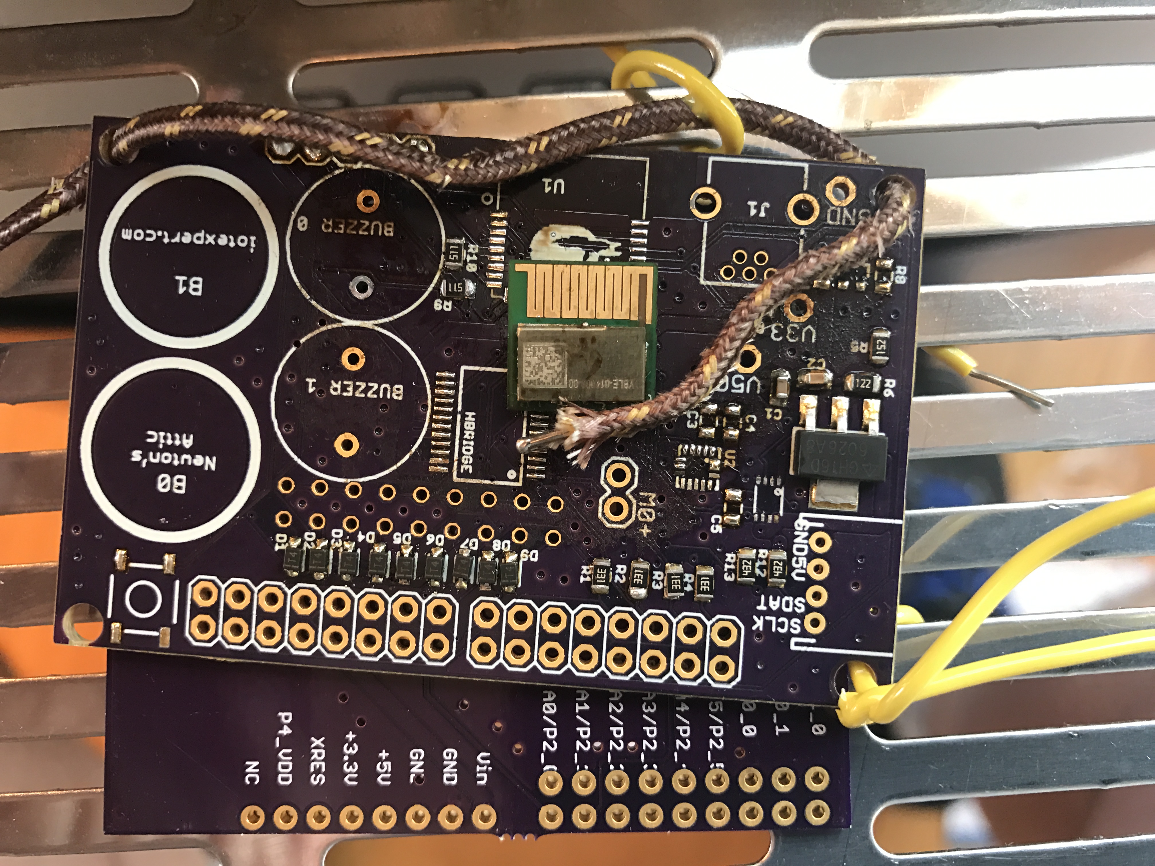
In the picture below, the PCB has been through about 15 reflows (which is why it looks so crappy).  The yellow wires are holding the board and the thermocouple wire in place.

img_3392

The modification that I made to the Cy8CKIT-025 kit example project were

  • Add the EZI2C Component

screen-shot-2016-11-27-at-10-26-23-am

  • Make a floating point buffer and attach it to the I2C

screen-shot-2016-11-27-at-10-27-20-am

  • Save the thermocouple data into the floating point buffer

screen-shot-2016-11-27-at-10-27-34-am

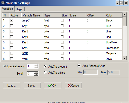
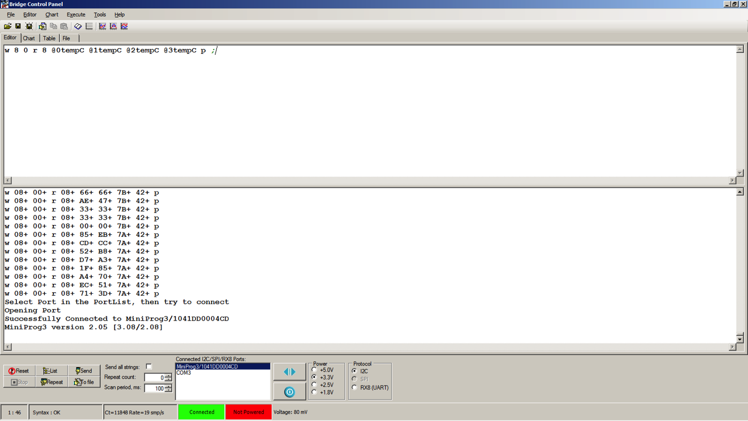
Once that was done, I can start the Bridge Control Panel and set it up to automatically read from the I2C by first setting up the variable tempC, setting up the read and then setting up the 100ms repeat.

screen-shot-2016-11-27-at-10-50-45-am

bcp

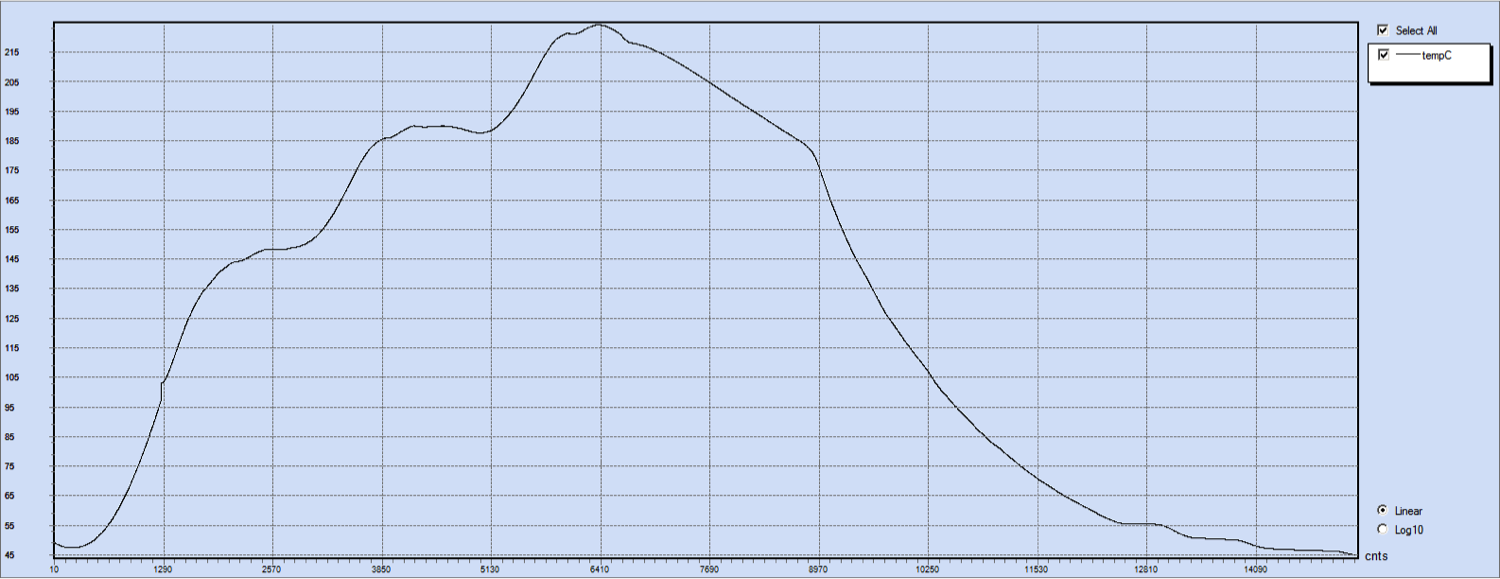
Now, I can run the whole thing and view the chart.

bcpgraph

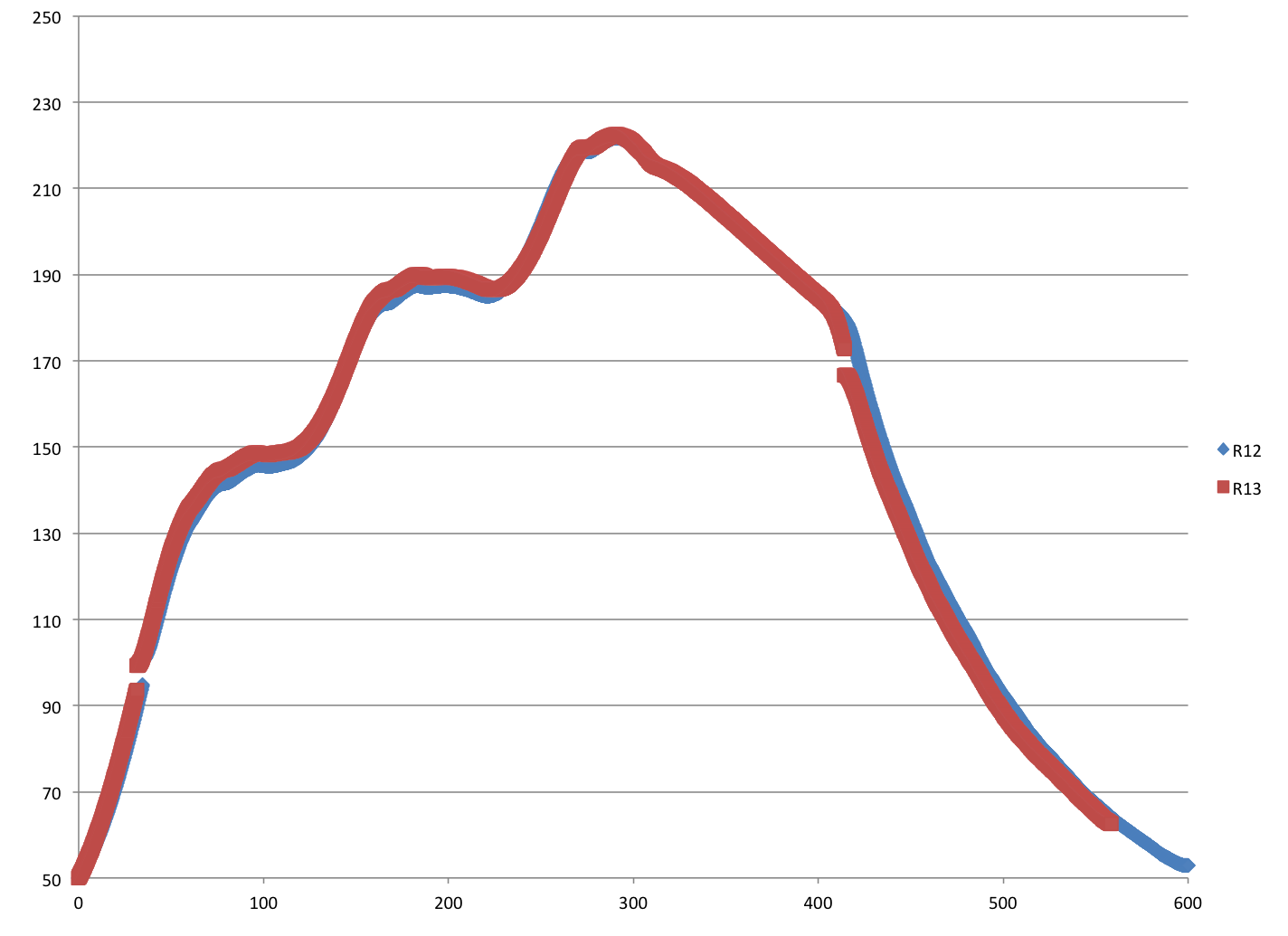
All of the temperature measurement is setup, so I can take some real data.  First I look for repeatability by running a couple of heat cycles.  The oven seems to act the same way every time here is an overlay of the 12th and 13th run.  (bad Alan… label your axis)

data-overlay

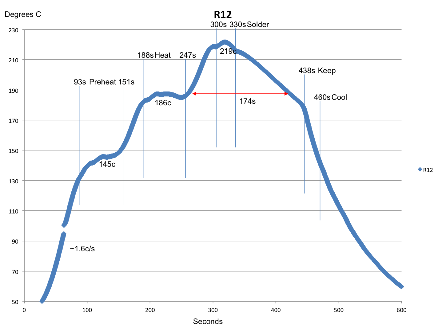
And finally we are ready to do a little bit of analysis.  Here is an annotated plot of Run12 which was done with the Lesnet profile:

  • Preheat 150 degrees 60 seconds
  • Heat 180 degrees 58 seconds
  • Solder 210 30 seconds
  • Keep 180 degrees
  • Cool 150 degrees

Based on the graph you can see that the oven seems to have 4 modes:

  1. Heat
  2. Hold
  3. Cool
  4. Cool with fan

In the graph below:

  •  The heater turns on to drive the temperature to the preheat phase (mode 1).  The oven heater appears to be able to raise the temperature linearly at about 1.6 degrees C per second.  Once it gets to the preheat temperature, it try’s to hold the temperature at about 145 degrees for 58 seconds (151-93) in mode 2.  Looking at the graph this section isn’t very flat, so I wonder if there is really a 5th mode?
  • The oven turns on the heater and the temperature ramps up to about 186 degrees (mode 1), which it then attempts to hold for about 60 seconds (mode 2)
  • Then the oven turns on the heater and raises the temperature to about 219 degree (mode 1), which it then holds for about 30 seconds (mode 2)
  • Then the oven lets the temperature drop naturally until it reaches about 180 degrees (mode 3)
  • Then the oven turns on the fans and drives the temperature in a steeper line down to 150 degrees (mode 4)
  • Then the oven turns off the fans and lets the oven cool down (mode 3)

analysis

As far as accuracy goes, the time measurement seems pretty good (one website bitched about this).  With regards to temperature it appears that the oven is a bit low during the preheat phase (which is also not very flat) and is a bit high during the heat and solder phases.  I think that I might lower the heat/solder temperatures a little bit.. 5 degrees?

As far as matching the Kester profile goes, or the the profile on the screenshot that Mr. Lesnet showed in his video, the heat/soak phase the temperature is just a little bit high.  However, he never says that his profile is intended for Sn63Pb37 solder so maybe he was trying to achieve something else (that is what I get for making an assumption).  The profile does however, work very well for me for that solder.  So where does that leave me?

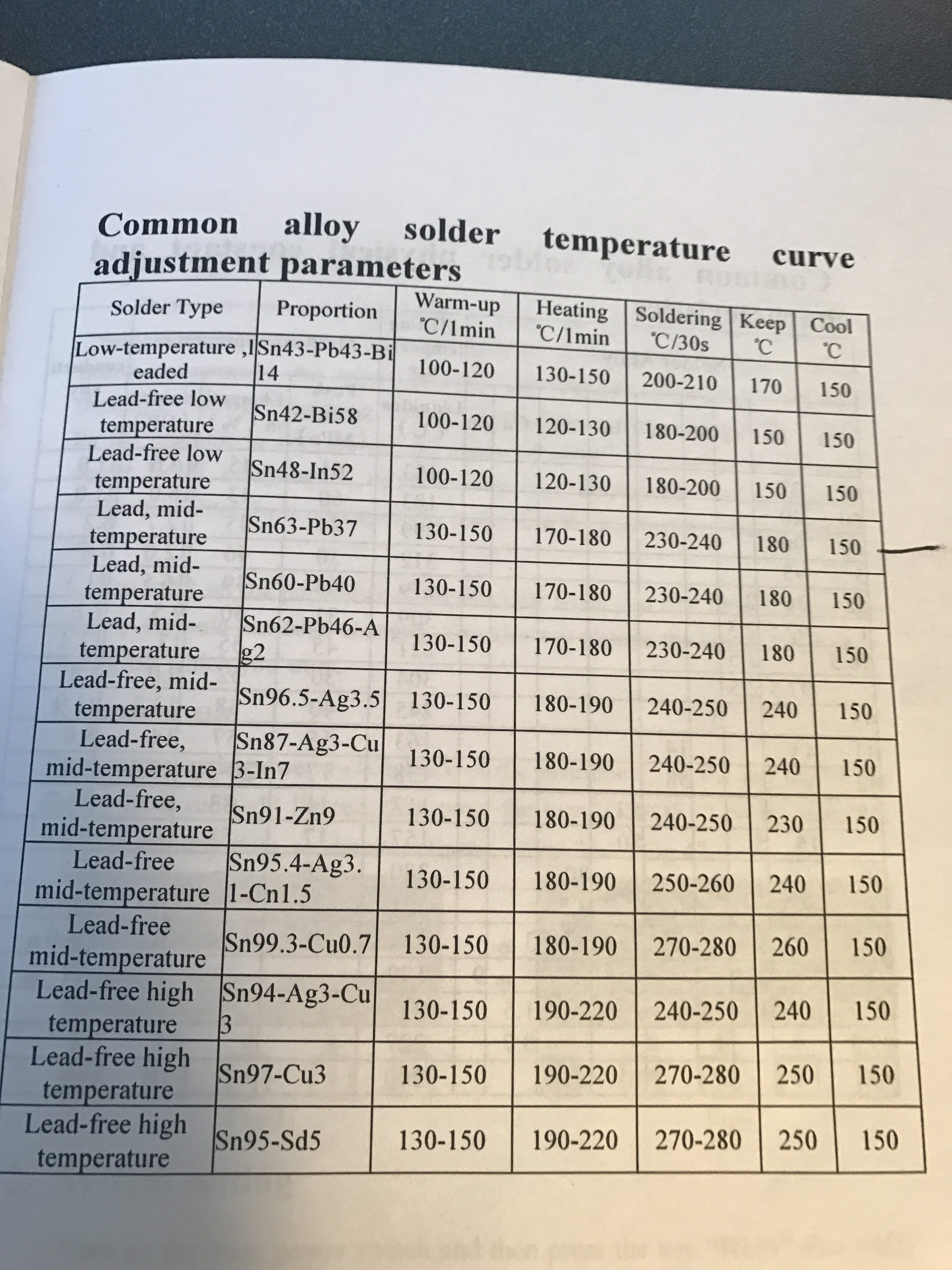
The book that came with the oven (which is obviously translated from Chinese into very funny English) says about the same numbers for the preheat and heat and a bit hotter for the solder.

img_3393

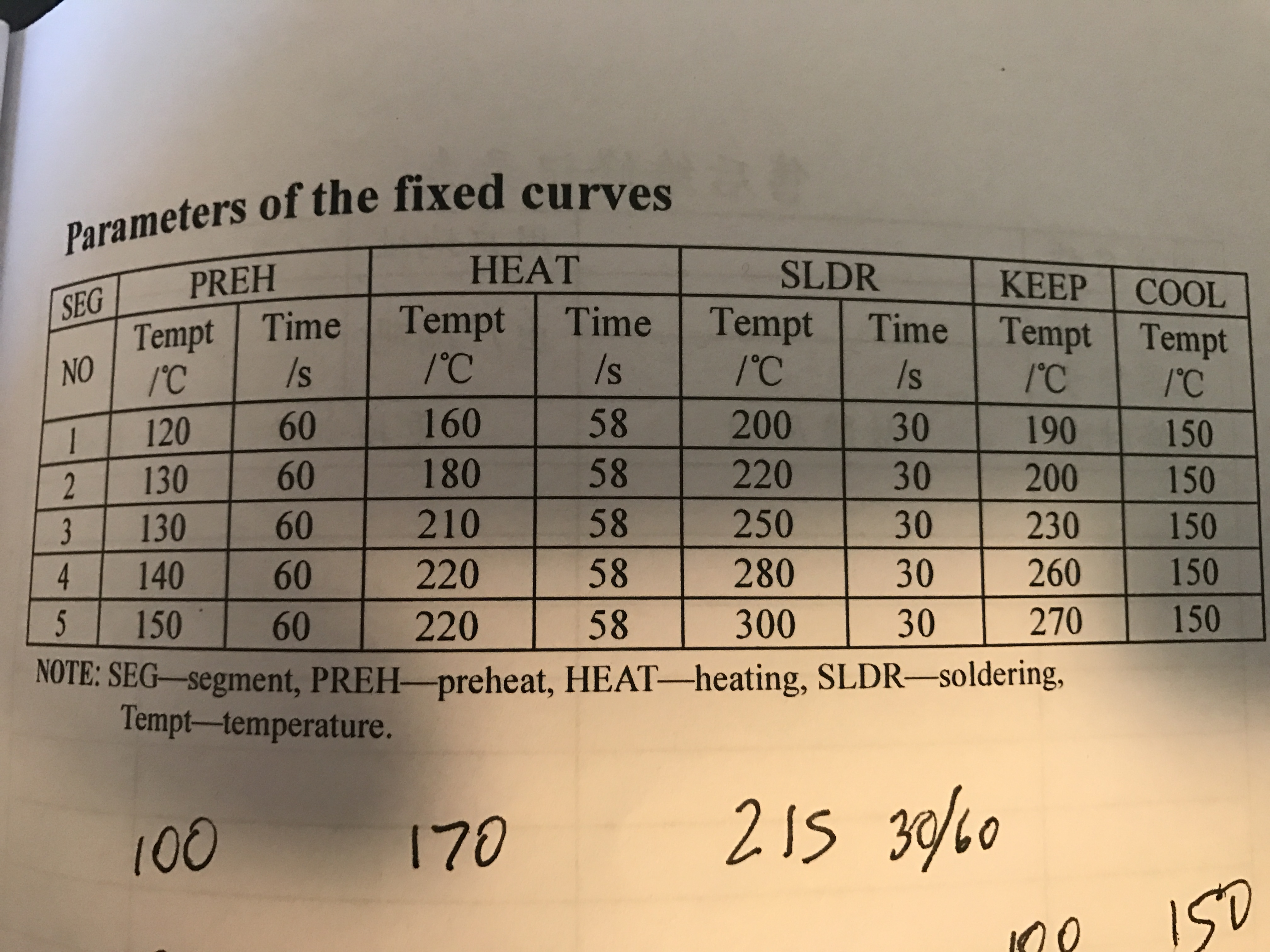
But interestingly, the oven does not come pre-programmed that way for any of the default profiles:

img_3394

The book that came with the oven also has a nice chart with some properties of different alloys of solder.  On that chart it says that the melting point of Sn63Pb37 is 183 degrees. That means that the soak/preheat phase is just below the melting point of the solder.  My best guess it that the spot where the thermocouple measures the temperature-just off of the surface of the board-is actually just touch higher than the actual junction temperature which is why I think that it works.

img_3396

The next real boards that I do I think that I will run an experiment and lower the preheat temperature by 5 degrees.  Unfortunately that still leaves me with the question… why did I have bad solder joints originally?  I think that the answer is old solder paste, but I am not sure that I will ever know.

That is it. While I was looking for information I found a number of resources on the internet to be useful

Link Comment
Ian Lesnet youtube video
Marks Tech Channel teardown of QS-5100 He warns you that a wire isn't connected properly
Kester Datasheet Graph profile on 2nd page of document
Reflow 7 youtube video A sweep of the temperature measured with a multi-meter
Dangerous Prototype Forum discussion a few solder profiles + some proposed modifications
MakeICT scan of QS-5100 manual Just a scan of the manual
An EEVBlog Forum discussion of the QS-5100 A bit of chatter
Despectus blog teardown of QS-5100 A modification of the placement of the thermocouple
Labitat wiki A few different reflow profiles & instructions