The Lost Art of Assembly Language Programming

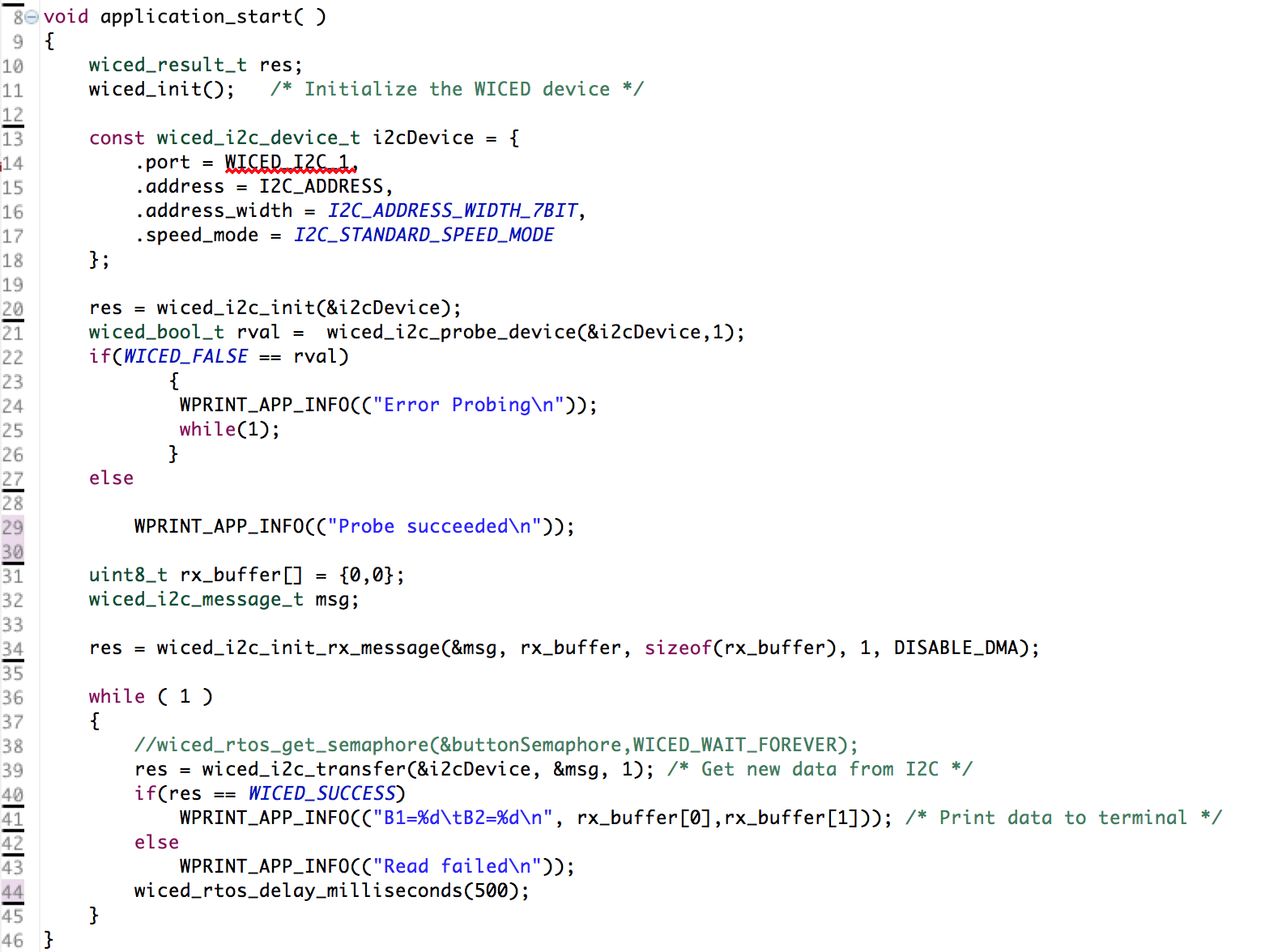
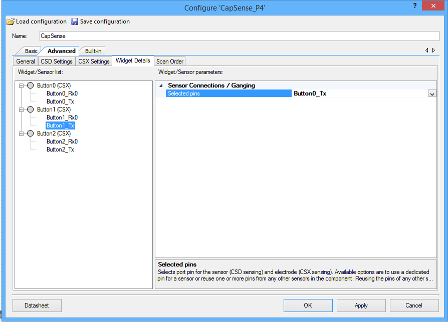
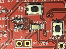
Cypress introduced it’s first mass market microcontroller in 2001. It used a Cypress designed 8 bit CISC processor running at 24 MHz, with as little as 4 KB Flash and 256 bytes RAM. Wrapped around that was a neat array of programmable analog and digital blocks. This may not sound like much, but with a creative mindset you could get these parts to do amazing things. For instance, I once implemented a complete ultrasonic ranging sensor with full wave analog demodulation in a single PSOC1 as shown below.

PSOC1 Ultrasonic Ranging

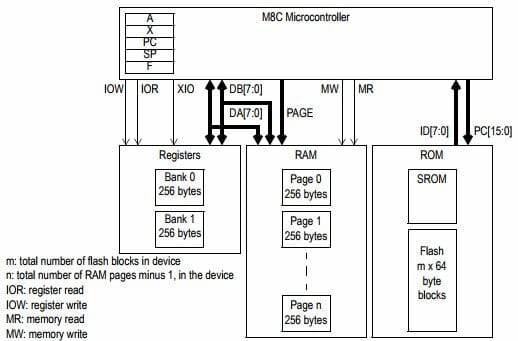
With CPU resources at a premium, you had to write tight, efficient code to get the most out of PSOC1. A single C library could consume the entire Flash. Consequently, I wrote a lot of assembly code. That’s not so bad, since I actually enjoy it more than C. There’s a certain elegance to well written, fully commented machine code. In the case of PSOC1, here’s what you had to work with: 5 registers, some RAM and Flash. That’s it. Real Men Write In Assembly.

M8C Architecture


We’ll start with simple machine code instruction to make the CPU do something. You can reference the M8C assembly language user guide here for more details. To get the M8C to execute 2+3=5 we write:

mov A,2       ;Load A with 2
add A,3       ;Add 3 to A. Result=5 is in A

We can get fancy by using variables. Let’s add R=P+Q. Assume P is at RAM location 0x20 and Q is at location 0x21, and R is at 0x22

;Initialize variables
mov [0x20],2  ;Load P with 2
mov [0x21],3  ;Load Q with 3

;Add variables
mov X,[0x20]  ;X <- P
mov A,[0x21]  ;A <- Q
adc [X],A     ;X <- P + Q
mov [0x22],X  ;R <- X

The fun thing about assembly is you can always dream up cool ways of doing things in less operations based on the machine’s instruction set. For example, we can simplify the above code as follows:

;Add variables
mov [0x20],[0x22]   ;R <- P
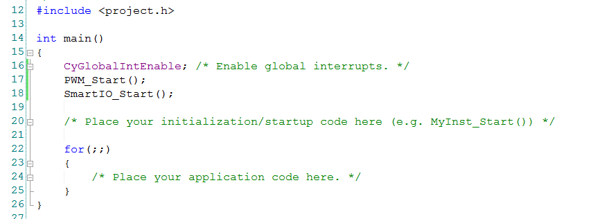
adc [0x22],[0x21]   ;R <- P + Q

In my experience, a good programmer with expert knowledge of the instruction set and CPU resources can always write better code than a compiler. There’s a certain human creativity that algorithms can’t match.

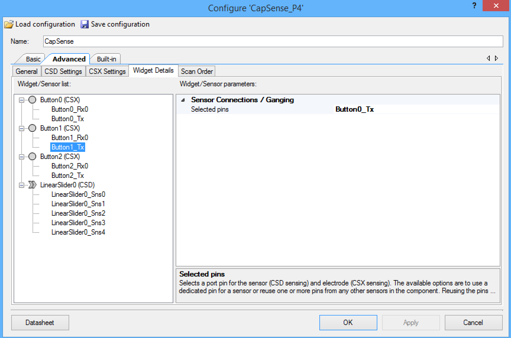
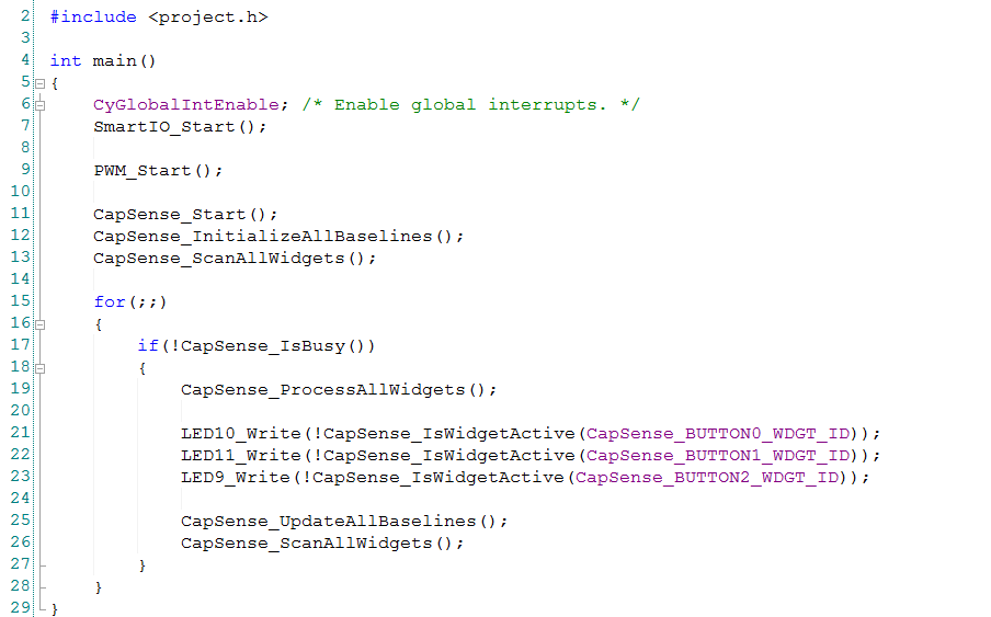
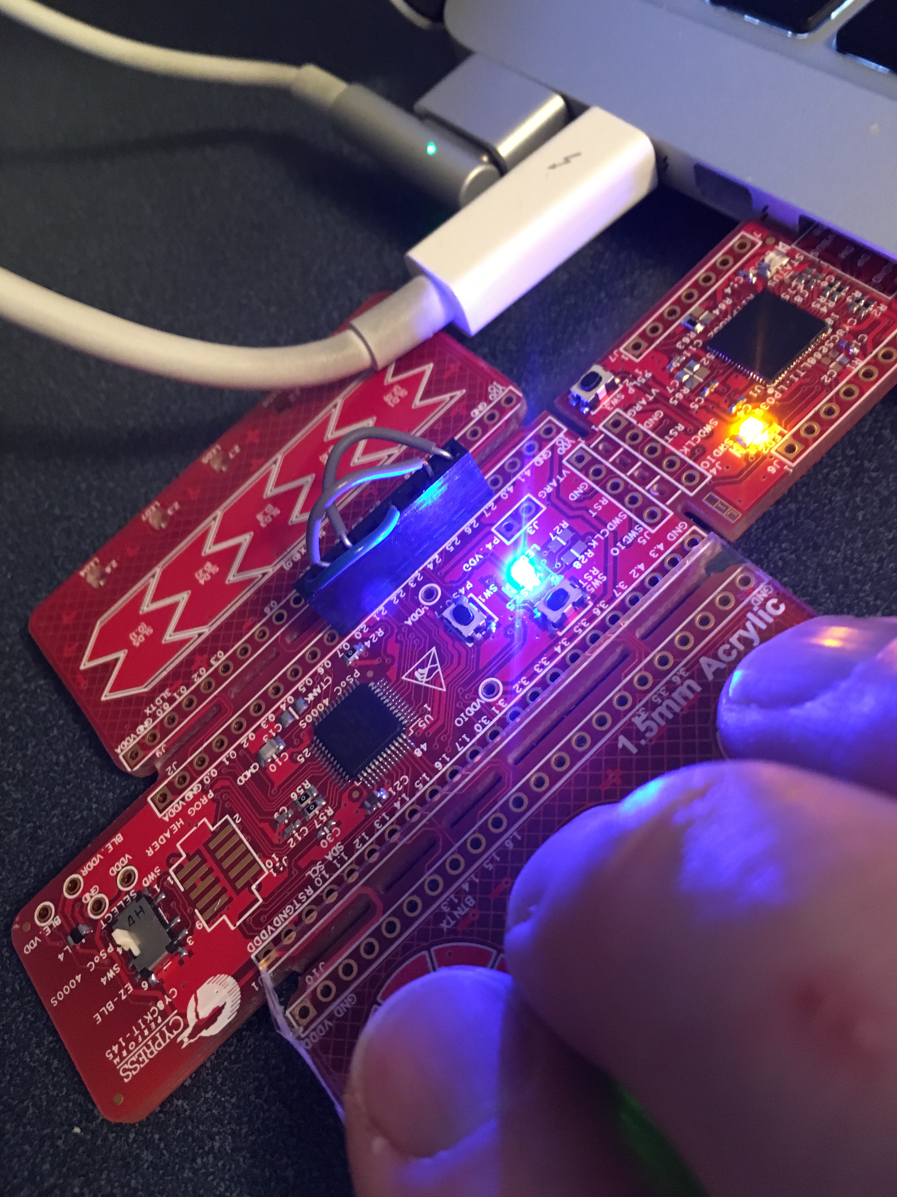
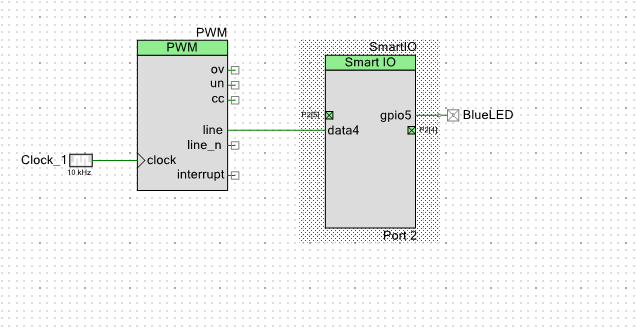
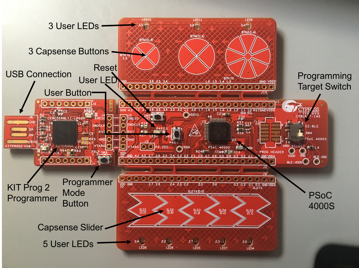
All that being said, I had not seen a good “machine code 101” tutorial for writing assembly in PSOC Creator on modern ARM M0 processors. So let’s walk through one now. We’ll use a CY8CKIT-145 and blink the LED. It’s just what happens to be laying around on the lab bench. Any PSOC4 kit will do.

CY8CKIT-145-40XX

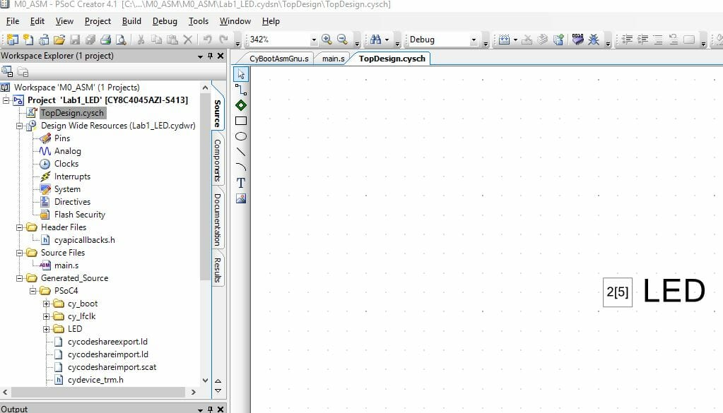
We’ll start by creating a standard project in PSOC Creator, drop a Digital Output pin on the schematic and call it “LED”

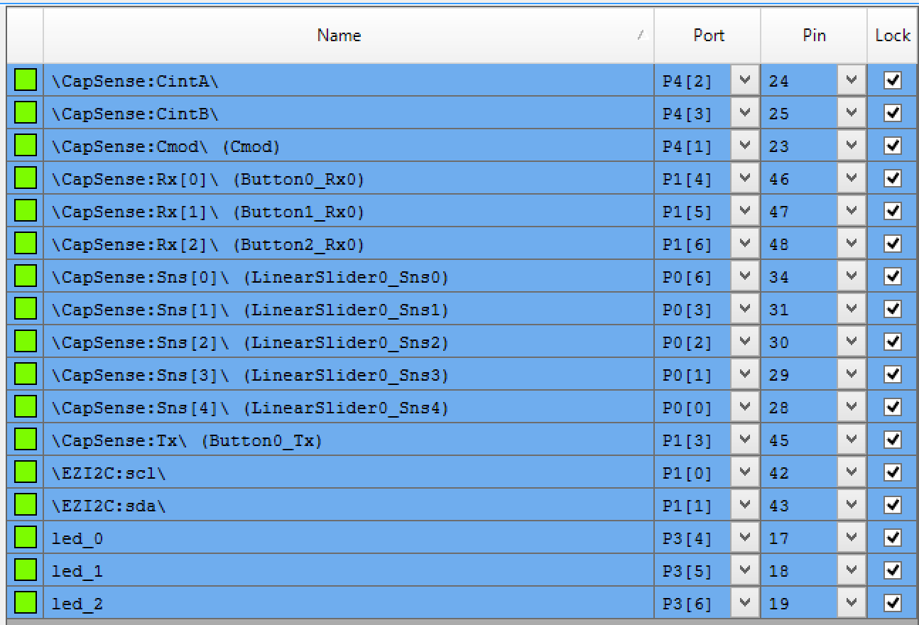
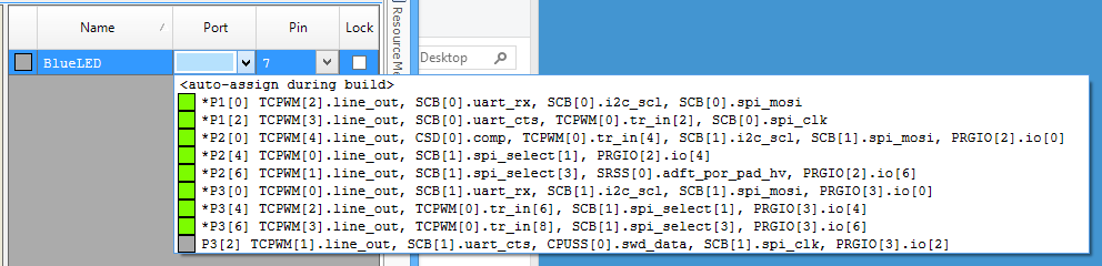
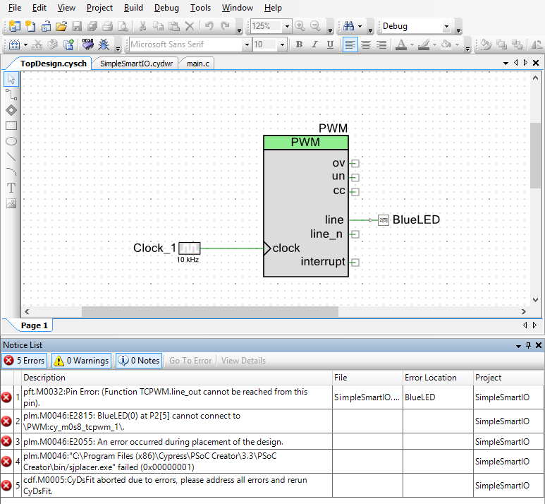
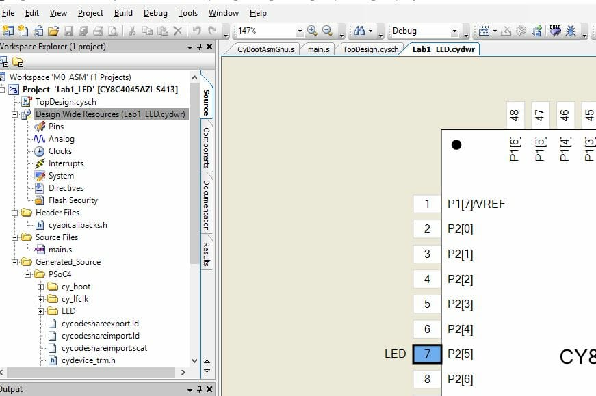
Then open the .CYDWR file and drag pin LED to P2[5], since that’s where it is on the LED board. Yours may be in a different place on whatever board you are using.

Now under “Source Files” in the workspace directory you will delete main.c and replace with main.s

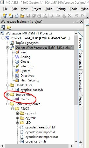
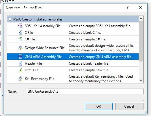
Now right clock on “Source Files”, select “Add New File” and select “GNU ARM Assembly File” in the dialog. Rename the file from GNUArmAssembly01.s to main.s

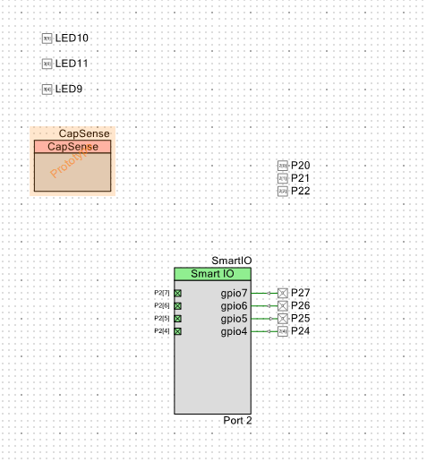
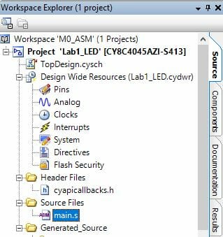
Your workspace ends up looking like this:

So far, so good. Now open main.s, delete everything if it’s not empty and add the following code. This sets up the IDE for M0 assembly architecture

// ==============================================
// ARM M0 Assembly Tutorial
//
// 01 – Blink LED
// ==============================================
.syntax unified
.text
.thumb

Next we need to include register definitions for the chip we are using. These are all from the PSOC4 Technical Reference Manual (TRM)

// ==============================================
// Includes
// ==============================================
.include “cydevicegnu_trm.inc”

Then we are going to do some .equ statements, same as #define in C. This identifies the Port 2 GPIO data register plus bits for the LED pin in on and off state

// ==============================================
// Defines
// ==============================================
.equ LED_DR,CYREG_GPIO_PRT2_DR          // LED data reg address
.equ LED_PIN,5                          // P2.5
.equ LED_OFF,1<<led_pin                 // 0010 0000
.equ LED_ON,~LED_OFF                    // 1101 1111

Now you add the right syntax to set up main()

// ==============================================
// main
// ==============================================
.global main
.func main, main
.type main, %function
.thumb_func

Finally we add the code for main, which is pretty simple:

main:
ldr r5,=LED_DR      // Load GPIO port addr to r5

loop0:
ldr r6,=LED_ON      // Move led data to r6
str r6,[r5]         // Write r6 data to r5 addr

ldr r0,=0xFFFFFF    // Argument passed in r0
bl CyDelayCycles    // Delay for N cycles

ldr r6,=LED_OFF     // Move led data to r6
str r6,[r5]         // Write r6 data to r5 addr

ldr r0,=0xFFFFFF    // Argument passed in r0
bl CyDelayCycles    // Delay for N cycles

b loop0             // Branch loop0

.endfunc            // End of main
.end                // End of code

One thing to note: The function CyDelayCycles is defined CyBootAsmGnu.s. Any function in assembly gets its arguments passed by the first 4 registers r0,r1,r2 and r3. Before calling the function you simply load r0 with the argument then do a bl (branch with link). This is also why I avoided the first 4 registers when messing with LED data. If you’re interested in doing more with ARM assembly, definitely read the Cortex M0+ Technical Reference Manual. It’s a great primer for the M0+ instruction set.

That’s it. End result is a blinking LED. Cool thing is you can use PSOC Creator with all it’s nice features, but sill access the power of machine code.

You can get the project ZIP file here.

Regards
Darrin Vallis

Electronica 2016 – CY8CKIT-145 User Interface

I finally made it to Munich late yesterday afternoon… then I proceeded to turn my hotel room into an electronics lab as I frantically worked to finish everything for tomorrow.  Earlier this year I wrote a whole series of posts about the PSoC4000S & CY8CKIT-145 after the Embedded World show.  We finally have volume production on the development kit and will be giving them out at the show this week.  So, I decided to use the -145 as part of the user interface for my Electronica project.  The devkit functions as the block labeled “PSoC Capsense”.  The wire between the “PSoC Capsense” and the “WICED WiFi” will be I2C (the green and red wire from the picture below)

electronica-wiced

The -145 devkit has the PSoC4000S silicon on it which has the new mutual capacitance capsense block.  On the devkit, there are three mutual cap buttons and one slider.  Here is a picture of the devkit connected to the WICED WiFi board that I am going to use:

img_3318

I want to make as simple of a PSoC Creator project as I can possibly do as I want to be able to easily do it live.  Here it is:

screen-shot-2016-11-07-at-10-12-23-am

The CapSense block is configured with three mutual cap buttons and 1 self-cap slider:

screen-shot-2016-11-07-at-10-13-54-am

On this development board, the three mutual cap buttons share the same transmit line, so you need to configure the component that way. The screen shot below shows the configuration of the “Button1_Tx” which is set to share the “Button0_Tx”.  You need to make the same setting for “Button2_Tx”.

screen-shot-2016-11-07-at-10-15-34-am

The next step is to assign all of the pins to the proper locations:

screen-shot-2016-11-07-at-10-18-10-am

Finally the smallest amount of firmware that I could think up to hold it all together.

Line 3-6: define a structure that the WICED board will be able to read.  It will represent the position of two of the Servo motors.  The CY_PACKED provides the compiler appropriate key words to make the bytes be right next to each other in the RAM, i.e. not word aligned..

Line 8: initializes both positions to 50%.

Lines 12-17 get the components going

Line 22: Checks to make sure that the CapSense block is not scanning before it reads the results

Line 24: Tells the CapSense block to process the results from the previous scan

Lines 25-31: Looks at the three buttons, sets the LEDs and sets pos1 to be either 25%, 50% or 75%

Line 33: Reads the position of the slider and assigns it to “pos0”

Lines 34-35: Gets the scanning going again

screen-shot-2016-11-07-at-10-21-02-am

To test the system I first used the bridge control panel.  First, connect to the kitprog2.  Then I setup a read from the I2C address (0x08) which is the address of my board.  I then click repeat which runs the read command over and over again.  In the picture below you can see that I tested the three position of the button (25,50 and 75 which are also known as 0x19, 0x32 and 0x4B).  Then I tested the slider by touching it about in the middle (0x3A)

screen-shot-2016-11-07-at-10-31-52-am

The next thing to do was make sure that the WICED devkit could read my I2C slave, so I wrote some WICED firmware to read the I2C registers every 500ms:

screen-shot-2016-11-07-at-10-55-08-am

But, occasionally I  was getting a “read failed”:

screen-shot-2016-11-07-at-10-58-48-am

Last night in my sleep deprived state I was struggling like crazy to figure it out.  This morning after some sleep I realized that the WICED board that I have must not like getting its I2C clock stretched.  So, I changed the priority of the I2C interrupt on the PSoC and that fixed the problem:

screen-shot-2016-11-07-at-10-28-03-am

Keep watching here for more updates on the project.

PSoC4000s & The SmartIO – Part 5

This is my last post on the SmartIO.  This time, I am going to describe how to use the SmartIO to trigger an interrupt.  For this project I will start from the “SmartIOCountUp” project.  That project is a 3-bit counter.  I thought that I would choose one of the states (000) and trigger an interrupt when that state is hit, then toggle the P25 user led.  I will keep data4, and gpio 3,6,7 exactly the same.  I will use gpio 2 to trigger the interrupt, which can be accomplished by setting it up as an output.  Here is the SmartIO configuration:

smart-io-config

The next step is to use LUT2 to look for the “000” state and to create a rising edge.  The other states will be 0.

lut-p22

After making the modification to the SmartIO the next step is to fix the schematic.  To do this I add a pin for P22, its configuration is on the next screen.  In addition I move the P25 (aka the BlueLED on the master board) to pin by itself.

interrupt-schematic

To configure the P22 pin.  There is a trick that is required to make the pin be both an output, so that it can be connected to the SmartIO LUT as well as an Input, so that it can be connected to the Port 2 interrupt.

pin-config

After setting up the pin to be both an Input and an Output you need to configure the pin to have an interrupt on the rising edge.

int-pin

Then I assign the pins.

interrput-pin-assignment

The last step is to make the firmware.

  • Lines 4-9 create an interrupt service routine
  • Line 18 registers the interrupt service routine to be called with the Port2 interrupt is triggered
  • The rest is the same as before

int-mainc

When I run this, I see the Blue LED toggle each time it gets to state 000 (which is all three LEDs on as they are active low).

You can find this PSoC Creator workspace on github in the directory called “SmartIO”.  This project is called “SmartIOInterrupt”.

Index Description
PSoC4000s & The SmartIO – Part 1 An introduction to the SmartIO and first project
PSoC4000s & CSX Mutual CapSense Buttons Part 1 Using mutual capacitance
PSoC4000s & CSX Mutual CapSense Buttons Part 2 Using the CapSense tuner
PSoC4000s & The SmartIO – Part 2 A 3 input XOR logic gate
PSoC4000s & The SmartIO – Part 3 A 3 bit up counter state machine
PSoC4000s & The SmartIO – Part 4 Using an external clock with the Smart IO
PSoC4000s & The SmartIO – Part 5 Triggering an interrupt

PSoC4000s & The SmartIO – Part 4

In the previous post I built a 3-bit counter that is clocked by the PWM.  In this example I will show you how to make the same design work with an external clock.  It seems like it would be cool to use the CapSense Button to provide the clock.  I will start by copying SmartIOCountUp to a new project called SmartIOCountUpExtClock.

First, I delete the clock and PWM.  Then add a new digital output pin (P20) that I can toggle from the CapSense handler and a digital Input pin (P21) to clock the SmartIO.  I add a wire between them on the female header on the board.

The next step is to modify the SmartIO.  I change data4 and data5 to bypass.  Then make gpio1 an input and then set the Clock to gpio1.  Here is what the new SmartIO configuration looks like:

smart-io-config

And the schematic.

smart-io-schematic

Assign the pins.

smart-io-dwr

I need to update the main.c write the CapSense button to P20 to be a clock source for the SmartIO

mainc

After I program the board, I can “clock” my statemachine with CapSense Button2.  Cool.  Obviously this example is a bit contrived in that I am running a wire on the outside of the chip, but you could imagine that you might have a “real” example that uses an onboard clock source.

You can find this PSoC Creator workspace on github in the directory called “SmartIO”.  This project is called “SmartIOCountUpExtClock”.

Index Description
PSoC4000s & The SmartIO – Part 1 An introduction to the SmartIO and first project
PSoC4000s & CSX Mutual CapSense Buttons Part 1 Using mutual capacitance
PSoC4000s & CSX Mutual CapSense Buttons Part 2 Using the CapSense tuner
PSoC4000s & The SmartIO – Part 2 A 3 input XOR logic gate
PSoC4000s & The SmartIO – Part 3 A 3 bit up counter state machine
PSoC4000s & The SmartIO – Part 4 Using an external clock with the Smart IO
PSoC4000s & The SmartIO – Part 5 Triggering an interrupt

PSoC4000s & The SmartIO – Part 3

For this post, I wanted to build a simple state machine inside of the SmartIO.  So I decided to build a 3-bit counter.  On the CY8CKIT145 board, port 2 is mostly connected to LEDs.  When you look at the picture below you can see that the LEDs on the left side of the board are easiest to see, so I decided to use them to indicate the state of the counter.  You can see from my notes that I was originally considering using LED9,11,10 which are the three LEDs on the CapSense buttons board.  I also considered using LED5,6,8 which are on the right side of the slider board, but I ruled all of that out because they were hard to see.

IMG_2737

To build this project you start by creating the schematic.  In this case I copied the design from the previous post called “145MutualCap” which had 3 CapSense buttons and 3 LEDs (LED10,11,9).  I then added:

  • A 5 KHz Clock to drive the PWM
  • A PWM to divide down the clock to a speed that I could see and provide a clock for the counter
  • A Smart IO
  • 4 Output Pins to drive LEDs (P27, P26, P25, P23)

counter-schematic-1

Next I configured the PWM with a 50% duty cycle and a Period of 10000.  This results in a 0.5Hz clock:

smartiopwm

Then I configure the SmartIO.

  • Setup “data4” as an input to the Smart IO.  Data 4 is the line out 0 of the TCPWM0
  • Setup “data5” as an input to the Smart IO.  Then configure it to be the “clock” for the smart IO. Data 5 is the Line_N of TCPWM0.  Originally I wanted to be able to have the clock drive LED5 as well, but this can create a timing hazard in the Smart IO and is not allowed (which is why I mirror data 4 onto the output P25.
  • Setup GPIO 7,6,5, and 3 as outputs (these outputs are connected to P27, P26, P23 which are the LEDs on the slider board.  GPIO5 is connected to P25 that is the user LED on the main board

smartioconfig

Then I configure LUTs 6, 3, 7 to implement the state table of a counter

state

lut6

lut3

lut7

I want to be able to see the clock (the PWM input data4) ticking so I create a transparent LUT (000 = 0 and 111 = 1) for LUT5 which is attached to P25 which is the LED on the main board.

lut5

After this is done I need to assign the Pins.

smartiopinassignment

Followed by the very simple firmware which is copied from the previous design.  The only new code is line 9 to turn on the PWM.

main

You can find this PSoC Creator workspace on github in the directory called “SmartIO”.  This project is called “SmartIOCountUp”.

Index Description
PSoC4000s & The SmartIO – Part 1 An introduction to the SmartIO and first project
PSoC4000s & CSX Mutual CapSense Buttons Part 1 Using mutual capacitance
PSoC4000s & CSX Mutual CapSense Buttons Part 2 Using the CapSense tuner
PSoC4000s & The SmartIO – Part 2 A 3 input XOR logic gate
PSoC4000s & The SmartIO – Part 3 A 3 bit up counter state machine
PSoC4000s & The SmartIO – Part 4 Using an external clock with the Smart IO
PSoC4000s & The SmartIO – Part 5 Triggering an interrupt

PSoC4000s & The SmartIO – Part 2

In the previous posts I introduced you to the Smart IO.  I also went through the instructions to create CapSense Buttons using the new Mutual-cap CSX mode of the PSoC4000S.  In this post I am going to use the three CapSense buttons on the CY8CKIT-145 as inputs to the Smart IO.  I want to create a simple logic function P25 = !XOR(P24,P26,P27).  This will cause the LED that is attached P25 to light up when there is an odd number of 1’s on P24,P26,P27.  The equation is slightly strange because the LED is wired as active low (it lights up when there is a 0 written to it)

To make this work I soldered an 8 pin female header to Port 2 of my development kit.  I then wired:

  • P20 <–> P24
  • P21 <–> P26
  • P22 <–> P27

You can see all of that in the picture below.

IMG_2744

The next step is to create the schematic for this design.  I started from the Mutual Capacitance project that I talked about in the previous post.  It has three LEDs and the Capsense Buttons.  I then add

  • Three digital output pins (P20,P21,P22) to drive the three inputs to the SmartIO
  • Three digital input pins (P24,P26, P27) to use as inputs to the SmartIO
  • One digital output pin (P25) to drive the LED
  • The Smart IO block

3xorschematic

The next step is to configure the SmartIO.  I setup P24,P26,P27 as “inputs” and setup P25 as an “output”

smartio-config

Then I configure the LUT to match the logic equation: P25 = !XOR(P24,P26,P27)

LUT5

Lastly I assign the pins to the correct physical pins on the chip.

dwr

Then I create the firmware by copying the main.c from the earlier CapSense example.  I then add the small amount of code to glue it all together:

  • Line 7: start the SmartIO
  • Lines 27-29: Write to P20,P21,P22 based on the state of the input buttons.

3xormainc

You can find this PSoC Creator workspace on github in the directory called “SmartIO”.  This project is called “3Xor”.

In the next post I will show you how to make a state machine using the Smart IO.

Index Description
PSoC4000s & The SmartIO – Part 1 An introduction to the SmartIO and first project
PSoC4000s & CSX Mutual CapSense Buttons Part 1 Using mutual capacitance
PSoC4000s & CSX Mutual CapSense Buttons Part 2 Using the CapSense tuner
PSoC4000s & The SmartIO – Part 2 A 3 input XOR logic gate
PSoC4000s & The SmartIO – Part 3 A 3 bit up counter state machine
PSoC4000s & The SmartIO – Part 4 Using an external clock with the Smart IO
PSoC4000s & The SmartIO – Part 5 Triggering an interrupt

PSoC4000s & CSX Mutual CapSense Buttons Part 2

In the previous post I gave you the instructions to get the new Mutual Capacitance buttons going on the CY8CKIT-142.  In this post I will talk about how to add the Capsense Tuner to your project.  The Capsense tuner can talk to your design while it is running, then report back to you the parametric of your design.

First you need to add the tuner to your project.  In order to do this, start with the last design, then add an EzI2C component.  Here is the new schematic:

Tuner-Schematic

Then you configure the EZ2IC to have 16 bit sub addresses.

Tuner-EzConfig

Then assign the EZI2C pins to the KitProg I2C bridge pins

Tuner-DWR

The last step is to write the firmware which is almost exactly what you had in the last project except

  • Lines 8-9 which start the capsense block and setup the Capsense memory buffer to be readable by the remote host
  • Line 21: which updates the Capsense memory buffer with the current state of the capsense parameters

tuner-firmware

Once all of this is done, build and program the device.  Then start the capsense tuner by right clicking the Capsense component in the schematic and saying “run Tuner”

launch-tuner

Then configure the tuner communication parameters from the “Tools->Tuner communication setup” menu.  These should match what you have setup in the EZI2C component.  Specifically you need set the I2C addresses to be the same, and you need to have the sub-address set to “2-bytes” which is the same as the 16-bit sub-address which you set in the component above.

tuner-comm-setup

The next step is to press “connect”  and the “start”.  First make sure that your three buttons are working.  In the picture below you can see that I am touching Buttons 1 and 2 as they are “active” (red color) which means that their signal is above the threshold.

2-buttons

The next step is to look at a “graph view” of button 0.  You can do this by pressing “graph view” and selecting Button0_Rx0.  Once I switch to this view I touch the button 9 times.  You can see that as there are 9 button touches in the Status window.  A status of 1 means that the button is active and a status of 0 is an inactive.

In the sensor data window you can see the “baseline” which is the noise on the sensor node without a touch.  The blue line is the “RawCounts” which the amount of signal on the node.

In the middle window you can see the “Sensor Signal” which is the Sensor Data minus the baseline.  Any time the Sensor Signal is above the touch threshold then the sensor status is active.

Tuner-graph

The last step is to use the SNR measurement tab to see how robust your design is.  First click on the “SNR Measurement” tab.  Then pick out which sensor you will measure.  In this case I have setup measurement on “Button_0”.  Then click on “Acquire noise” and wait.  It will make the graph shown below which says that my noise is about 3008-2995 or about 13 counts.

BaselineNoise

The next step is to see how much signal you get.  Start this process by pressing “Acquire Signal” and touching the correct button.  You can see orange line represents the amount of signal when you are touching the sensor.  The system will then calculate the SNR which in this case is 56.85 which is tons.

SNR

The last thing that you could do is change the Capsense parameters in the sensor parameter screen.  For instance you could change the threshold from 100 to a bigger number to give more reliable touches.

Parameters

OK.  Now I have my capsense buttons working.  In the next posts Ill be ready to talk more about the Smart IO.

You can find this PSoC Creator workspace on github in the directory called “145MutualCap”.  This project is called “TunerMutualCapButtons-145”.

PSoC4000s & CSX Mutual CapSense Buttons Part 1

In the previous post I talked about my original goal to learn about the SmartIO.  But, in order fully try out the SmartIO I needed an input source.  On this board I had only one easy input from the factory – specifically the mechanical button on P0[7]- but I wanted to have multiple switches.  Well, the obvious choice was to use the three Capsense Buttons on the user interface expansion board.   When I looked at that board closely I remembered that the buttons were put there to support the new Capsense functionality of the PSoC4000s family.  Inside of Cypress we call the new feature “CSX”, but its real name is “Mutual Capacitance”.  Mutual Capsense works by transmitting a signal on the “Tx” pin and then receiving that signal by capacitively coupling that signal through your finger into the “Rx” line.  Here is a picture of that part of the PCB schematic and a zoom in of the board.  You can see that there are three different size buttons.  Each of the buttons is composed of an even number of pie shaped segments.

mutual-cap-buttonsScreen Shot 2016-03-06 at 2.03.17 PM

The mutual capacitance technique has a much higher Signal-to-Noise Ratio (SnR) as compared to the Self Capacitance technique of previous chips and as a result is more immune to noise and can work through a thicker overlay.  I thought that I would try putting on overlay on my board, so I cut out a piece of 1.5mm acrylic and used double sided tape to attach it to my board.  You can see it in the photograph above.

To make this work I started by creating a new project called “MutualCapButtons”.  I then added the Capsense component and three digital output pins (one for each of the three LEDs on the expansion board).  Here is the schematic:

mutual-button-schematic

The next step was to configure the CapSense block by double clicking it.  I then added three buttons and set the sensing mode to CSX (Mutual-cap).

mtutual-cap-config

It is possible to have dedicated Tx/Rx pins or you can share the Txs.  To do this, select “Advanced” and “Widget details”.  Then select “Button1_Tx”  and choose its sensor to be the same as “Button0_Tx”.  On this design I shared the Tx between all three of the buttons.

Mutual-sharing

The next step is to assign the pins to the correct Port/Pin locations on the chip:

button-pin-assignments

The last step is to write the firmware

  • Lines 8-10 Start the capsense block and get the scanning going
  • Line 14: If the capsense block is done scanning then process the results
  • Line 16: Take all of the raw data from the scan and setup all of the status information
  • Lines 18-20: If the buttons are being pushed then turn on the corresponding LED
  • Lines 22-23 Start another scan

Mutual-firmware

That is all there is to making it work.

You can find this PSoC Creator workspace on github in the directory called “145MutualCap”.  This project is called “MutualCapButtons-145”.

In the next post Ill talk in detail about using the Capsense Tuner to understand the Capsense performance.

PSoC4000s & The SmartIO – Part 1

In the previous four posts I talked about building an IOT device using the new CY8CKIT145.  You might remember from the first post that my original objective in picking up the board was to try a new feature of PSoC Creator.  Well, over the last few days I have been trying out that feature. Actually, it isn’t a feature of the software, it is a feature of some of the new chips called the Smart IO.  The Smart IO is a programmable logic bock that sits between the High Speed IO Matrix (HSIOM) of the chip and the Input/Output Port.  The HSIOM has all of the peripherals (SCB, TCPWM etc) of the chips attached to it.  The Smart IO will allow you to take signals from inside or outside of the chip, perform logic functions on them, and then drive those signals into or out of the chip.  Some of examples of why you might want to do this include:

  • Combining several inputs (from the outside) to trigger an interrupt
  • Inverting a signal entering the chip
  • Inverting a signal exiting the chip
  • Remapping an input from one pin to a different input (e.g. flipping Tx, Rx pins)
  • Buffering one signal into multiple output pins (to increase the drive strength)

As usual with Cypress programmable logic, you can do a jaw dropping number of clever things.  This block includes sequential logic as well as combinational logic, so it is possible to make state machines in the fabric.  It also includes more surprises which have not been shown yet.

The Smart IO works the same as other peripheral blocks, you start by dragging the component onto the schematic and double clicking to start the customizer.

When you start the customizer you get the screen below.  The first thing to decide is which Port is going to use the Smart IO.  The Smart IO completely takes over an entire port.  On this chip there are two Smart IOs, one on Port 2 and one on Port 3.   When you look at the customizer there are some things to notice:

  • On the right side of the customizer you can see the 8 GPIO pins.  The dropdown menus that are currently labeled “Bypass” allow you to select the mode of the pin (Bypass, Input, Output, None).
  • On the bottom of the customizer you can see the 8 LUTs and select their inputs.
  • On the left side of the customizer you can see the the 8 connections to/from the HSIOM.  The drop down menu that is currently labeled “Bypass” allows you to select the mode of that connection to the HSIOM (Bypass, Input, Output, None).   I will talk about the “Undefined” menu in the with the next picture
  • In the middle of the customizer is the routing matrix.  Horizontally on the routing matrix there are 8 groups of three wires.  The top wire in each group is a wire that originates with the GPIO.  The middle wire originates from the corresponding LUT.  The bottom wire originates from the HSIOM.  For example the top three wires in the picture are
    • Line 1: from GPIO7
    • Line 2: from LUT 7
    • Line 3: from Data7
  • You can “make” the connection by either by clicking the solder dot or by choosing from the coresponding drop down menu (more on that below)

basicsmartio

The other menu on the HSIOM side of the customizer says “Undefined”.  This menu has a list of each fixed function device and the inputs/outputs of that device that can be connected to that input/output.  This menu doesn’t actually change anything in your design, it is only for information.  For example you can see in the screen shot below that  data4 can connect to:

  • TCPWM0: Line_Out
  • LCD0: COM[20]
  • LCD0: SEG[20]
  • SCB1: Spi Select[1]

smartio-dataselect

The best way to show you how all this works is with an example.  One of the frustrating things for me in the PSoC 4 Family has always been that the fixed function blocks (TCPWM, SCB) are only allowed to connect to a few pins on the chip.  This can be a bit of a pain if you have a board that is already wired and you need to remap a pin.  Take for example, on the Cy8CKIT-145 the user LED on the main board is connected to P2[5].  If I want to drive that LED with the Line out (instead of the Line_Out_N) I would create a schematic like this:

BlueLEDSchematic

When I go to the DWR to assign the pins I would see that the BlueLED cannot be attached to P2[5].  You can see all of the legal placements of that pin because they are highlighted in green.

blueledpinassignment

If I try to do it anyway, I will get the following error when I build.

pwm_error

This error says that I cannot connect the “line” output of the TCPWM to P2[5] (the pin with the LED).  That sucks.  But, with the Smart IO, I can “remap” the TCPWM Line output to P2[5].  To do this, I will start with a by adding a SmartIO to my schematic and configuring it.

  1. Select Port 2
  2. Configure GPIO 5 to “Output”.  This can be done by either clicking on the “solder dot” or by selecting output from the drop down menu
  3. Select data 4 as “Input”
  4. Select data 4 as “TCPWM[0].line.  Remember that this is ONLY for your information and doesn’t actually change anything in the project.
  5. Select the 3 inputs to LUT5 to be the data4 line which can be done from the three drop down menus or by clicking the three corresponding solder dots.

Screen Shot 2016-03-06 at 9.53.10 AMNext, I configure the LUT to “passthrough” by setting up 000 = 0 and 111=1 (which are the only two possible combinations as the three inputs are tied together).  You change the “Out”s from 0->1 and 1->0 by clicking on it.

LUT5

Then I will re-wire up the schematic to look like this:

blue-led-schematic-smartio

The firmware is trivial,  just start the PWM and the SmartIO

blue-led-firmware

When I program the kit the blue LED starts blinking.  Cool.

In the next posts I will teach you how to use some other configurations of the Smart IO and how to use the CapSense block to create inputs for the Smart IO.

You can find this PSoC Creator workspace on github in the directory called “SmartIO”.  This project is called “SimpleSmartIO”.

Index Description
PSoC4000s & The SmartIO – Part 1 An introduction to the SmartIO and first project
PSoC4000s & CSX Mutual CapSense Buttons Part 1 Using mutual capacitance
PSoC4000s & CSX Mutual CapSense Buttons Part 2 Using the CapSense tuner
PSoC4000s & The SmartIO – Part 2 A 3 input XOR logic gate
PSoC4000s & The SmartIO – Part 3 A 3 bit up counter state machine
PSoC4000s & The SmartIO – Part 4 Using an external clock with the Smart IO
PSoC4000s & The SmartIO – Part 5 Triggering an interrupt

PSoC4000s and the CY8CKIT145 Stamp Board – Part 4

OK.  We’re ready for the big moment: the user test.  I was feeling pretty cool.  I had spent the week talking to 100s of people and putting on a pretty good show.  I was the master of all things PSoC, a geek rockstar.  So I programmed the firmware.  The slider worked.  I was able to connect to the PRoC BLE from my app.  But for some stupid reason the the PSoC and PRoC just were not talking and I had no idea why.  And to make matters worse, I didn’t have anything I could (easily) use to debug the problem.   So much for being the king of PSoC.  I assumed that I had firmware bugs. I tried a bunch of different things, single stepping code, trying different pins, etc.  But nothing worked.  I couldn’t figure it out.  It was intensely frustrating to be stuck on the airplane with a broken design.

As soon as I landed in Detroit, I logged in to get my email.  I looked for messages from Rajesh (the PSoC Kit Manager) and sure enough, he had emailed me the missing schematic.  After digging through the schematic, I found the error.

schematic-resistors

The connection between the PRoC and PSoC had a 0 Ohm resistor that was “No Load,” meaning the footprint was there, but the board manufacturer had not put on the resistor.  This was done so that the pin could be used as a GPIO for something else.

Here is a zoomed-in picture of the PCB:

missing-resistors

The good news was, I was only one plane ride and an hour drive from my soldering iron.  As soon as I walked in the door, I went straight to my lab.

fixed-resistors

Now everything works.

There are two morals to this story:

  1. Don’t go to immediately to your lab after being gone for a week, as it really irritates your wife.
  2. Look closely at the schematic.

You can find the PSoC Creator workspace on github in the directory called “capsenseble-145.”

PSoC4000s and the CY8CKIT145 Stamp Board – Part 3

In this post, I will take you through the PRoC BLE schematic and firmware.  I describe a very similar version to this in great detail in the video you can find on the Cypress Video Training website.

First, I create a new project in my workspace called “145capsenseled-ble.”  Then, I add the UART component (the SCB version) and the BLE component.

schematic

Next, I configure the component to be a GATT server with a custom profile and a GAP client.

overall-profile

Then I create a custom service with two characteristics:

  • The “led” characteristic, which is set up as a uint8 that is writeable and readable.
  • The “capsense” characteristic, which is set up as uint16 that is readable and has a “notify.”

Next, I configure the UUIDs of the service and characteristics to match what is hard-coded in the iOS app.  Then, I add “Client User Descriptions” that describe the characteristics in plain text.

gatt-settings

Next I configure the GAP settings, specifically the advertising packet.

advertising-packet

I make the pin I assignments, which is just the UART Rx and Tx lines.

dwr-pin-assignment

Finally, I write the firmware.  I started with main.  In the infinite loop (line 116), if I have received a byte from other side, then I assign it to the global variable “fingerPos” (line 118). Next, call updateCapsense() (line 119), to update the GATT database with the new value of the slider.

main

The updateCapsense function:

Lines 31/32 If there is no connection, then don’t update the GATT database.

Lines 33-39 Update the GATT database with the current fingerPosition.

Lines 42-43 If the iPhone side has asked for notification and the position has changed, then send a notification.

Line 44 Save the last position.

update-capsense

The BleCallBack is the most complicated section of firmware.  It uses a “switch” statement to handle the different event “cases.” The cases are:

  • CYBLE_EVT_STACK_ON & CYBLE_EVT_GAP_DEVICE_DISCONNECTED:  In either of these cases you want to start the advertising function.
  • CYBLE_EVT_GATT_CONNECT_IND: When there is a connection made, update the GATT database with the current state of the CapSense and the LED.  This allows the iOS side to read the correct values.
  • CYBLE_EVT_WRITE_REQ: There are two kinds of write requests that are valid.
    • CYBLE_LED_CAPSENSE_LED_CHAR_HANDLE:  If the remote side writes into the LED value, then send that data to the PSoC4000S via the UART.
    • CYBLE_LEDCAPSENSE_CAPSENSE_CAPSENSECCCD: If the remote side has been asked to notify (or un-notify), then save that in the global variable capsenseNotify.

ble-callback

That is all of the firmware.

In the next post, I’ll take you through the debugging I had to do.

You can find the PSoC Creator workspace on github in the directory called “capsenseble-145.”

PSoC4000s and the CY8CKIT145 Stamp Board – Part 2

In the previous post, I unboxed the CY8CKIT145 and showed you the schematics.   In this post, I will show you how to build the CapSense firmware that runs on the PSoC4000S.  The first decision I needed to make was how to connect the PSoC and the PRoC chips.  So I looked at the back of the kit and there was a handy-dandy picture of the schematic in the silkscreen.  Here is a zoomed in view:

zoom-145

I didn’t have the schematic on the airplane, but here is a more “schematic” view of the chips on the board.

systemschematic-c


I knew that the UART source code would be slightly easier, so I picked that as the mechanism to connect the chips.  On my computer I had the “capsenseled” workspace from the videos.  So, I created a new PSoC4000S project in that workspace called “145capsenseled.”  I started with the schematic:

  1. Add the new CapSense component.  I am currently running a “nightly build” of PSoC Creator 3.3 that supports the new chip.  You can see in the PSoC Creator release I’m using there is a prototype version of the CapSense component.
  2. Add 5 Digital Output Pins under software control to drive the LEDs that are next to the slider
  3. Add 1 Digital Output pin to drive the blue LED
  4. Add a Serial Communication Block (SCB) configured as a UART

capsenseled-schematic

Here is a screenshot of the new CapSense component configuration wizard.  You can see I added a linear slider and set up the component to use SmartSense full-auto tuning.

capsense-configuration

After configuring the CapSense, I set up the pin assignments using the DWR:

capsenseled-pinassignment

Then I wrote the firmware, which was pretty straight forward.

  • 10-11 start the CapSense
  • 12 start the UART
  • 16: If the CapSense block is done scanning and is idle, then read the CapSense and do something with it (lines 17 -> 41).
  • 18: figure out where the person is touching
  • 19: if they have actually touched the block
  • 22-26 light up the LEDs
  • 30-35 If there is no touch, then turn off the LEDs.
  • 36-37 start the next scan
  • 38-39: If the UART is not busy… then send the position (0-100) or (0xFF if there is no touch).
  • 41-42: If there is a byte in the UART receive buffer, then light up or turn off the Blue LED. (Notice that the LED is active low so I use the “!” operation to flip the state of the signal.

capsense-firmware

After that, I programmed the kit and tested it.  It seemed like everything was good.  In the next post, I’ll show you the schematic and firmware that runs on the PRoC BLE.

You can find the PSoC Creator workspace on github in the directory called “capsenseble-145.”

PSoC4000s and the CY8CKIT145 Stamp Board – Part 1

One of the cool things about my job is I get to try out lots of new development kits before they are released to the general public.  In the previous post I talked about the demonstration I gave at the Embedded World conference using the CY8CKIT-042 BLE.  You can find a complete video tutorial for that project on the cypress.com video tutorial website.  While I was at the conference, I picked up an engineering sample of a new development kit and put it into my backpack because I wanted to try a new feature of PSoC Creator on the way home.  But, when I got on the airplane, I thought I would build the same project I had demonstrated at the conference using this kit.  So, in the next few posts, I am going to show you the new CY8CKIT145 Stamp Board and how to build an IOT solution with it.

It is called a “stamp board” because it comes in a flat postage stamp-like postcard mailer.  Here is a picture of the front and the back (you can see that it has already lived a hard life riding around in my backpack).

IMG_2720

Here is the back of the mailer:

IMG_2722

In the picture you can see the yellow label proclaiming this to be an engineering sample.  It doesn’t seem like much, but when you pull back the front of the package you get to see the surprise:

IMG_2721-1

The kit can literally be broken into four separate pieces:

  1. The main board:
    • The PSoC4000S
    • A reset switch
    • A user LED
    • A user push button
    • A programming selector (to pick either the PSoC4000s or the PRoC BLE (that is on the back of the kit)) as the target of the programmer
    • All of the PSoC4000S pins are available on the 100mil center headers
    • A PCB footprint for a 10-pin ARM programming header
  2. A programmer board:
    • A PSoC5LP programmed with KitProg2 Firmware
    • A programmer mode button
    • 100mil center header with some of the PSoC5LP pins
  3. A Capsense slider user interface board with a 5 Segment Slider and 5 LEDs
  4. A Capsense button user interface board with 3 mutual capacitance buttons and 3 LEDs

145front-e

And the back, with the tiny 10mm X 10mm PRoC BLE module:

IMG_2706

Here is the schematic for the board:

CY8CKIT-145_PSOC_4A-S1-page1

CY8CKIT-145_PSOC_4A-S1 page 2

CY8CKIT-145_PSOC_4A-S1-page3

I wanted to build a project that would have two-way communication between my iPhone and the board, and would be compatible with the Swift App I had written.  The user of the board would have a capsense slider (and LEDs) of which the iPhone App could read the position.  In addition, it would have an LED that the iOS app could turn on and off.  Here is a demonstration that I filmed with my iPhone on the airplane:

In the next post I will describe the overall system and show you the firmware.