PSoC4000s & The SmartIO – Part 5

This is my last post on the SmartIO.  This time, I am going to describe how to use the SmartIO to trigger an interrupt.  For this project I will start from the “SmartIOCountUp” project.  That project is a 3-bit counter.  I thought that I would choose one of the states (000) and trigger an interrupt when that state is hit, then toggle the P25 user led.  I will keep data4, and gpio 3,6,7 exactly the same.  I will use gpio 2 to trigger the interrupt, which can be accomplished by setting it up as an output.  Here is the SmartIO configuration:

smart-io-config

The next step is to use LUT2 to look for the “000” state and to create a rising edge.  The other states will be 0.

lut-p22

After making the modification to the SmartIO the next step is to fix the schematic.  To do this I add a pin for P22, its configuration is on the next screen.  In addition I move the P25 (aka the BlueLED on the master board) to pin by itself.

interrupt-schematic

To configure the P22 pin.  There is a trick that is required to make the pin be both an output, so that it can be connected to the SmartIO LUT as well as an Input, so that it can be connected to the Port 2 interrupt.

pin-config

After setting up the pin to be both an Input and an Output you need to configure the pin to have an interrupt on the rising edge.

int-pin

Then I assign the pins.

interrput-pin-assignment

The last step is to make the firmware.

  • Lines 4-9 create an interrupt service routine
  • Line 18 registers the interrupt service routine to be called with the Port2 interrupt is triggered
  • The rest is the same as before

int-mainc

When I run this, I see the Blue LED toggle each time it gets to state 000 (which is all three LEDs on as they are active low).

You can find this PSoC Creator workspace on github in the directory called “SmartIO”.  This project is called “SmartIOInterrupt”.

Index Description
PSoC4000s & The SmartIO – Part 1 An introduction to the SmartIO and first project
PSoC4000s & CSX Mutual CapSense Buttons Part 1 Using mutual capacitance
PSoC4000s & CSX Mutual CapSense Buttons Part 2 Using the CapSense tuner
PSoC4000s & The SmartIO – Part 2 A 3 input XOR logic gate
PSoC4000s & The SmartIO – Part 3 A 3 bit up counter state machine
PSoC4000s & The SmartIO – Part 4 Using an external clock with the Smart IO
PSoC4000s & The SmartIO – Part 5 Triggering an interrupt

PSoC4000s & The SmartIO – Part 4

In the previous post I built a 3-bit counter that is clocked by the PWM.  In this example I will show you how to make the same design work with an external clock.  It seems like it would be cool to use the CapSense Button to provide the clock.  I will start by copying SmartIOCountUp to a new project called SmartIOCountUpExtClock.

First, I delete the clock and PWM.  Then add a new digital output pin (P20) that I can toggle from the CapSense handler and a digital Input pin (P21) to clock the SmartIO.  I add a wire between them on the female header on the board.

The next step is to modify the SmartIO.  I change data4 and data5 to bypass.  Then make gpio1 an input and then set the Clock to gpio1.  Here is what the new SmartIO configuration looks like:

smart-io-config

And the schematic.

smart-io-schematic

Assign the pins.

smart-io-dwr

I need to update the main.c write the CapSense button to P20 to be a clock source for the SmartIO

mainc

After I program the board, I can “clock” my statemachine with CapSense Button2.  Cool.  Obviously this example is a bit contrived in that I am running a wire on the outside of the chip, but you could imagine that you might have a “real” example that uses an onboard clock source.

You can find this PSoC Creator workspace on github in the directory called “SmartIO”.  This project is called “SmartIOCountUpExtClock”.

Index Description
PSoC4000s & The SmartIO – Part 1 An introduction to the SmartIO and first project
PSoC4000s & CSX Mutual CapSense Buttons Part 1 Using mutual capacitance
PSoC4000s & CSX Mutual CapSense Buttons Part 2 Using the CapSense tuner
PSoC4000s & The SmartIO – Part 2 A 3 input XOR logic gate
PSoC4000s & The SmartIO – Part 3 A 3 bit up counter state machine
PSoC4000s & The SmartIO – Part 4 Using an external clock with the Smart IO
PSoC4000s & The SmartIO – Part 5 Triggering an interrupt

PSoC4000s & The SmartIO – Part 3

For this post, I wanted to build a simple state machine inside of the SmartIO.  So I decided to build a 3-bit counter.  On the CY8CKIT145 board, port 2 is mostly connected to LEDs.  When you look at the picture below you can see that the LEDs on the left side of the board are easiest to see, so I decided to use them to indicate the state of the counter.  You can see from my notes that I was originally considering using LED9,11,10 which are the three LEDs on the CapSense buttons board.  I also considered using LED5,6,8 which are on the right side of the slider board, but I ruled all of that out because they were hard to see.

IMG_2737

To build this project you start by creating the schematic.  In this case I copied the design from the previous post called “145MutualCap” which had 3 CapSense buttons and 3 LEDs (LED10,11,9).  I then added:

  • A 5 KHz Clock to drive the PWM
  • A PWM to divide down the clock to a speed that I could see and provide a clock for the counter
  • A Smart IO
  • 4 Output Pins to drive LEDs (P27, P26, P25, P23)

counter-schematic-1

Next I configured the PWM with a 50% duty cycle and a Period of 10000.  This results in a 0.5Hz clock:

smartiopwm

Then I configure the SmartIO.

  • Setup “data4” as an input to the Smart IO.  Data 4 is the line out 0 of the TCPWM0
  • Setup “data5” as an input to the Smart IO.  Then configure it to be the “clock” for the smart IO. Data 5 is the Line_N of TCPWM0.  Originally I wanted to be able to have the clock drive LED5 as well, but this can create a timing hazard in the Smart IO and is not allowed (which is why I mirror data 4 onto the output P25.
  • Setup GPIO 7,6,5, and 3 as outputs (these outputs are connected to P27, P26, P23 which are the LEDs on the slider board.  GPIO5 is connected to P25 that is the user LED on the main board

smartioconfig

Then I configure LUTs 6, 3, 7 to implement the state table of a counter

state

lut6

lut3

lut7

I want to be able to see the clock (the PWM input data4) ticking so I create a transparent LUT (000 = 0 and 111 = 1) for LUT5 which is attached to P25 which is the LED on the main board.

lut5

After this is done I need to assign the Pins.

smartiopinassignment

Followed by the very simple firmware which is copied from the previous design.  The only new code is line 9 to turn on the PWM.

main

You can find this PSoC Creator workspace on github in the directory called “SmartIO”.  This project is called “SmartIOCountUp”.

Index Description
PSoC4000s & The SmartIO – Part 1 An introduction to the SmartIO and first project
PSoC4000s & CSX Mutual CapSense Buttons Part 1 Using mutual capacitance
PSoC4000s & CSX Mutual CapSense Buttons Part 2 Using the CapSense tuner
PSoC4000s & The SmartIO – Part 2 A 3 input XOR logic gate
PSoC4000s & The SmartIO – Part 3 A 3 bit up counter state machine
PSoC4000s & The SmartIO – Part 4 Using an external clock with the Smart IO
PSoC4000s & The SmartIO – Part 5 Triggering an interrupt

PSoC4000s & The SmartIO – Part 2

In the previous posts I introduced you to the Smart IO.  I also went through the instructions to create CapSense Buttons using the new Mutual-cap CSX mode of the PSoC4000S.  In this post I am going to use the three CapSense buttons on the CY8CKIT-145 as inputs to the Smart IO.  I want to create a simple logic function P25 = !XOR(P24,P26,P27).  This will cause the LED that is attached P25 to light up when there is an odd number of 1’s on P24,P26,P27.  The equation is slightly strange because the LED is wired as active low (it lights up when there is a 0 written to it)

To make this work I soldered an 8 pin female header to Port 2 of my development kit.  I then wired:

  • P20 <–> P24
  • P21 <–> P26
  • P22 <–> P27

You can see all of that in the picture below.

IMG_2744

The next step is to create the schematic for this design.  I started from the Mutual Capacitance project that I talked about in the previous post.  It has three LEDs and the Capsense Buttons.  I then add

  • Three digital output pins (P20,P21,P22) to drive the three inputs to the SmartIO
  • Three digital input pins (P24,P26, P27) to use as inputs to the SmartIO
  • One digital output pin (P25) to drive the LED
  • The Smart IO block

3xorschematic

The next step is to configure the SmartIO.  I setup P24,P26,P27 as “inputs” and setup P25 as an “output”

smartio-config

Then I configure the LUT to match the logic equation: P25 = !XOR(P24,P26,P27)

LUT5

Lastly I assign the pins to the correct physical pins on the chip.

dwr

Then I create the firmware by copying the main.c from the earlier CapSense example.  I then add the small amount of code to glue it all together:

  • Line 7: start the SmartIO
  • Lines 27-29: Write to P20,P21,P22 based on the state of the input buttons.

3xormainc

You can find this PSoC Creator workspace on github in the directory called “SmartIO”.  This project is called “3Xor”.

In the next post I will show you how to make a state machine using the Smart IO.

Index Description
PSoC4000s & The SmartIO – Part 1 An introduction to the SmartIO and first project
PSoC4000s & CSX Mutual CapSense Buttons Part 1 Using mutual capacitance
PSoC4000s & CSX Mutual CapSense Buttons Part 2 Using the CapSense tuner
PSoC4000s & The SmartIO – Part 2 A 3 input XOR logic gate
PSoC4000s & The SmartIO – Part 3 A 3 bit up counter state machine
PSoC4000s & The SmartIO – Part 4 Using an external clock with the Smart IO
PSoC4000s & The SmartIO – Part 5 Triggering an interrupt

PSoC4000s & The SmartIO – Part 1

In the previous four posts I talked about building an IOT device using the new CY8CKIT145.  You might remember from the first post that my original objective in picking up the board was to try a new feature of PSoC Creator.  Well, over the last few days I have been trying out that feature. Actually, it isn’t a feature of the software, it is a feature of some of the new chips called the Smart IO.  The Smart IO is a programmable logic bock that sits between the High Speed IO Matrix (HSIOM) of the chip and the Input/Output Port.  The HSIOM has all of the peripherals (SCB, TCPWM etc) of the chips attached to it.  The Smart IO will allow you to take signals from inside or outside of the chip, perform logic functions on them, and then drive those signals into or out of the chip.  Some of examples of why you might want to do this include:

  • Combining several inputs (from the outside) to trigger an interrupt
  • Inverting a signal entering the chip
  • Inverting a signal exiting the chip
  • Remapping an input from one pin to a different input (e.g. flipping Tx, Rx pins)
  • Buffering one signal into multiple output pins (to increase the drive strength)

As usual with Cypress programmable logic, you can do a jaw dropping number of clever things.  This block includes sequential logic as well as combinational logic, so it is possible to make state machines in the fabric.  It also includes more surprises which have not been shown yet.

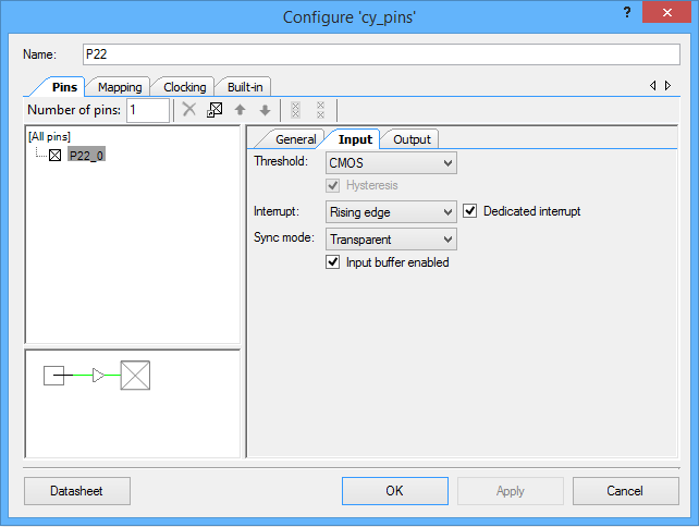
The Smart IO works the same as other peripheral blocks, you start by dragging the component onto the schematic and double clicking to start the customizer.

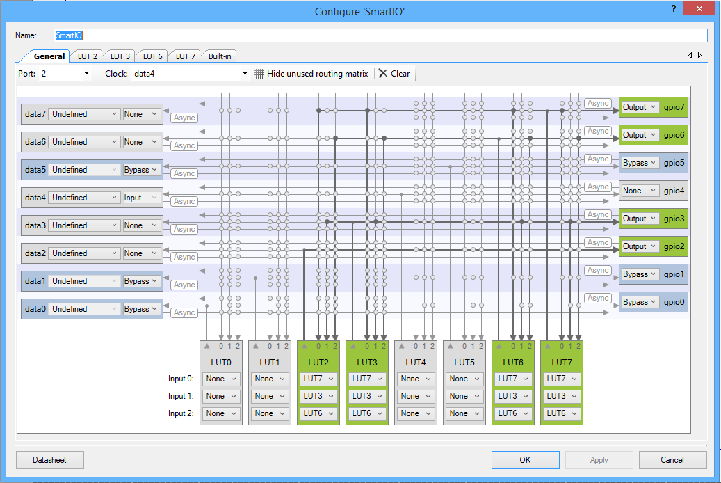
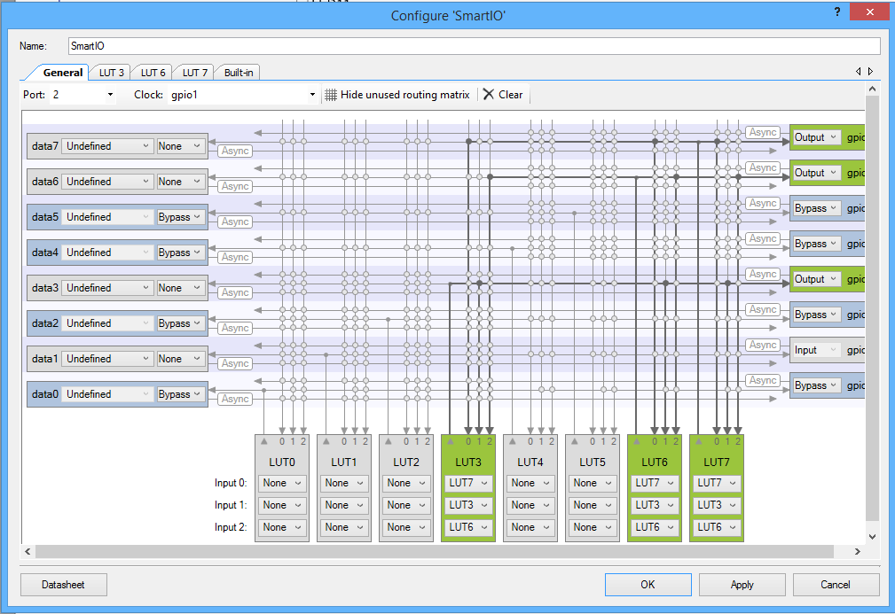
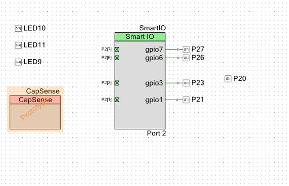
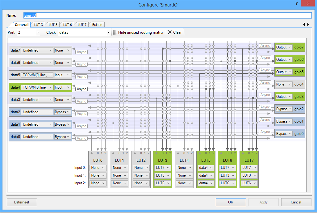
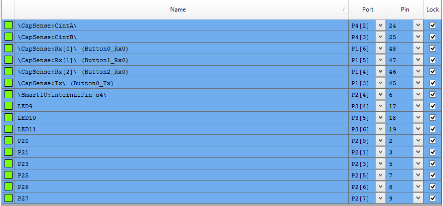
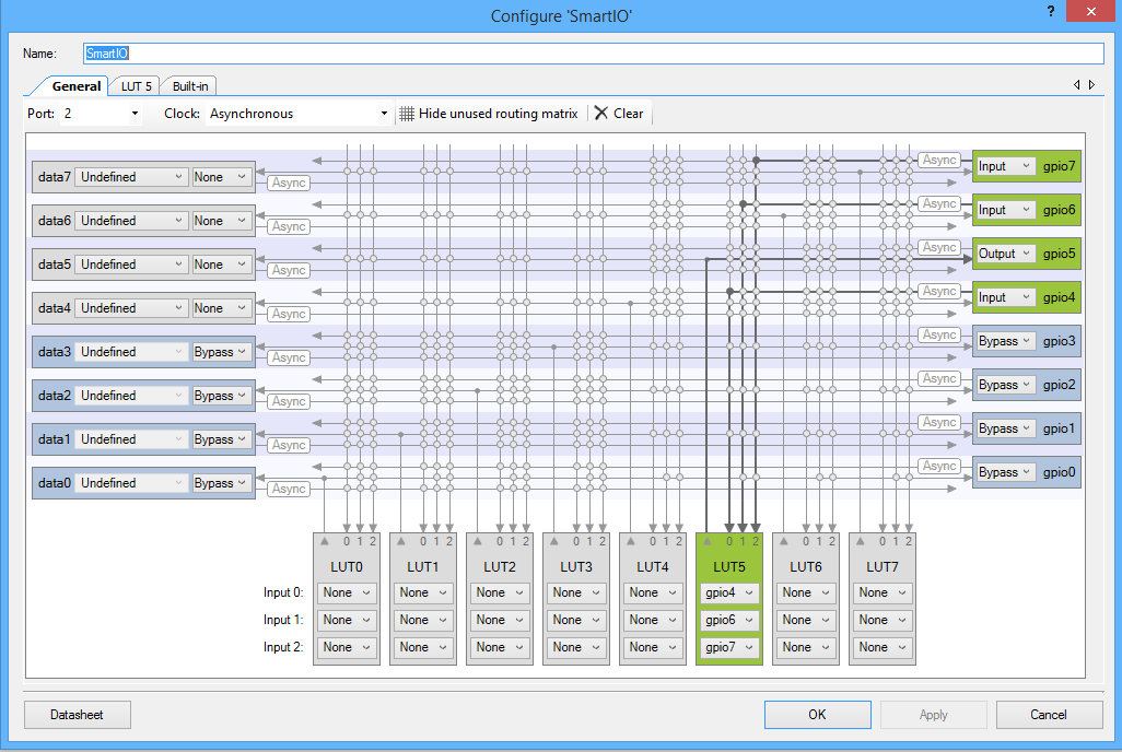
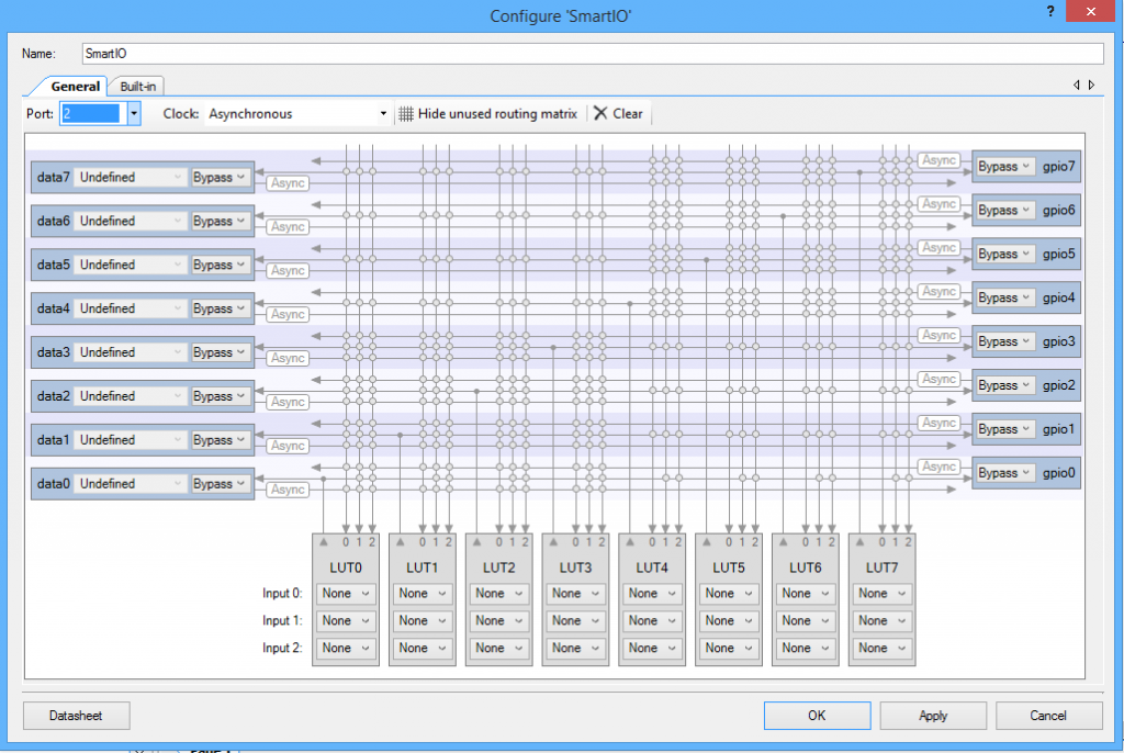
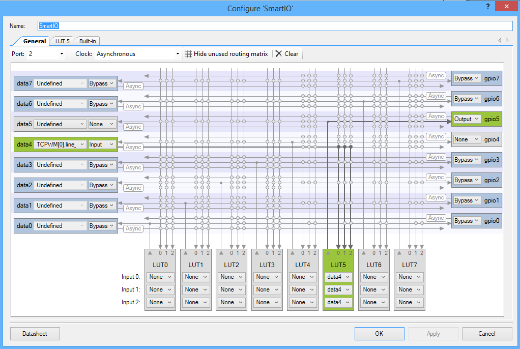
When you start the customizer you get the screen below.  The first thing to decide is which Port is going to use the Smart IO.  The Smart IO completely takes over an entire port.  On this chip there are two Smart IOs, one on Port 2 and one on Port 3.   When you look at the customizer there are some things to notice:

  • On the right side of the customizer you can see the 8 GPIO pins.  The dropdown menus that are currently labeled “Bypass” allow you to select the mode of the pin (Bypass, Input, Output, None).
  • On the bottom of the customizer you can see the 8 LUTs and select their inputs.
  • On the left side of the customizer you can see the the 8 connections to/from the HSIOM.  The drop down menu that is currently labeled “Bypass” allows you to select the mode of that connection to the HSIOM (Bypass, Input, Output, None).   I will talk about the “Undefined” menu in the with the next picture
  • In the middle of the customizer is the routing matrix.  Horizontally on the routing matrix there are 8 groups of three wires.  The top wire in each group is a wire that originates with the GPIO.  The middle wire originates from the corresponding LUT.  The bottom wire originates from the HSIOM.  For example the top three wires in the picture are
    • Line 1: from GPIO7
    • Line 2: from LUT 7
    • Line 3: from Data7
  • You can “make” the connection by either by clicking the solder dot or by choosing from the coresponding drop down menu (more on that below)

basicsmartio

The other menu on the HSIOM side of the customizer says “Undefined”.  This menu has a list of each fixed function device and the inputs/outputs of that device that can be connected to that input/output.  This menu doesn’t actually change anything in your design, it is only for information.  For example you can see in the screen shot below that  data4 can connect to:

  • TCPWM0: Line_Out
  • LCD0: COM[20]
  • LCD0: SEG[20]
  • SCB1: Spi Select[1]

smartio-dataselect

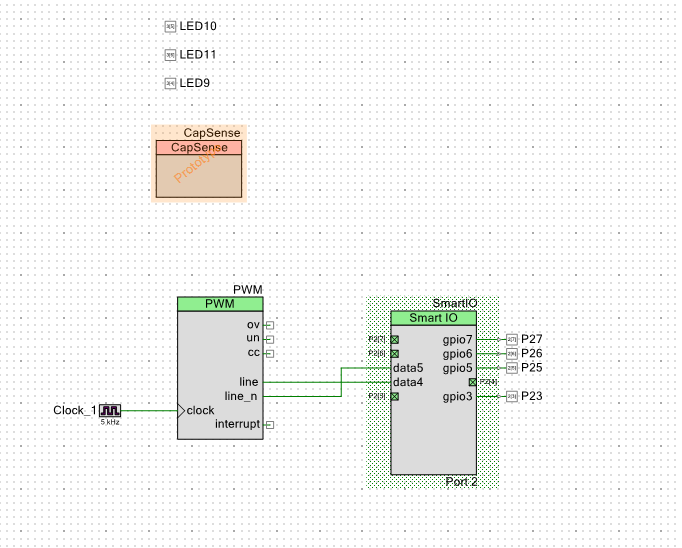
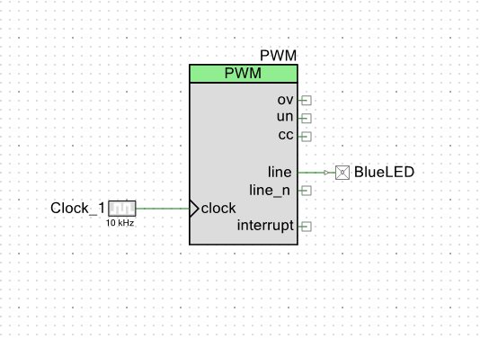
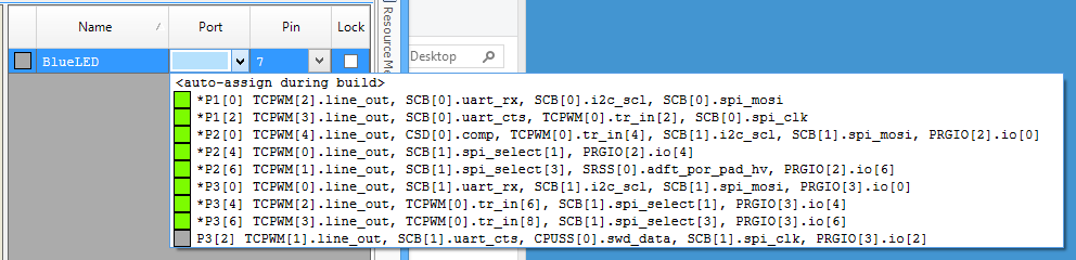
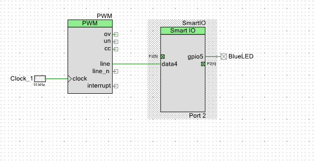
The best way to show you how all this works is with an example.  One of the frustrating things for me in the PSoC 4 Family has always been that the fixed function blocks (TCPWM, SCB) are only allowed to connect to a few pins on the chip.  This can be a bit of a pain if you have a board that is already wired and you need to remap a pin.  Take for example, on the Cy8CKIT-145 the user LED on the main board is connected to P2[5].  If I want to drive that LED with the Line out (instead of the Line_Out_N) I would create a schematic like this:

BlueLEDSchematic

When I go to the DWR to assign the pins I would see that the BlueLED cannot be attached to P2[5].  You can see all of the legal placements of that pin because they are highlighted in green.

blueledpinassignment

If I try to do it anyway, I will get the following error when I build.

pwm_error

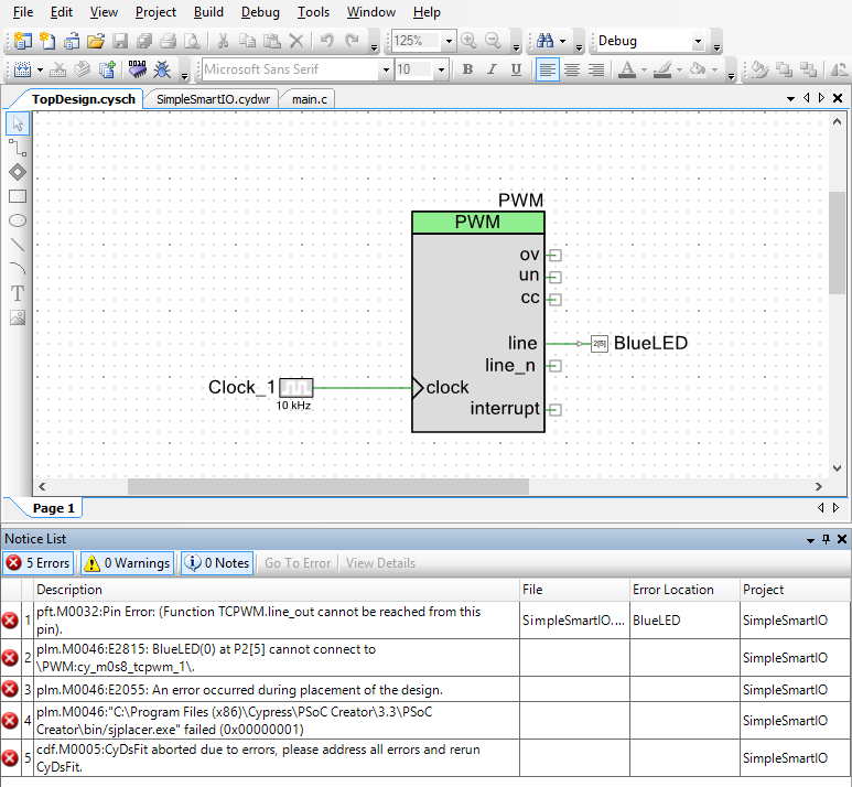
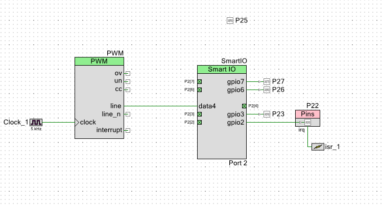
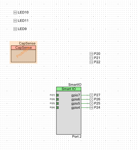
This error says that I cannot connect the “line” output of the TCPWM to P2[5] (the pin with the LED).  That sucks.  But, with the Smart IO, I can “remap” the TCPWM Line output to P2[5].  To do this, I will start with a by adding a SmartIO to my schematic and configuring it.
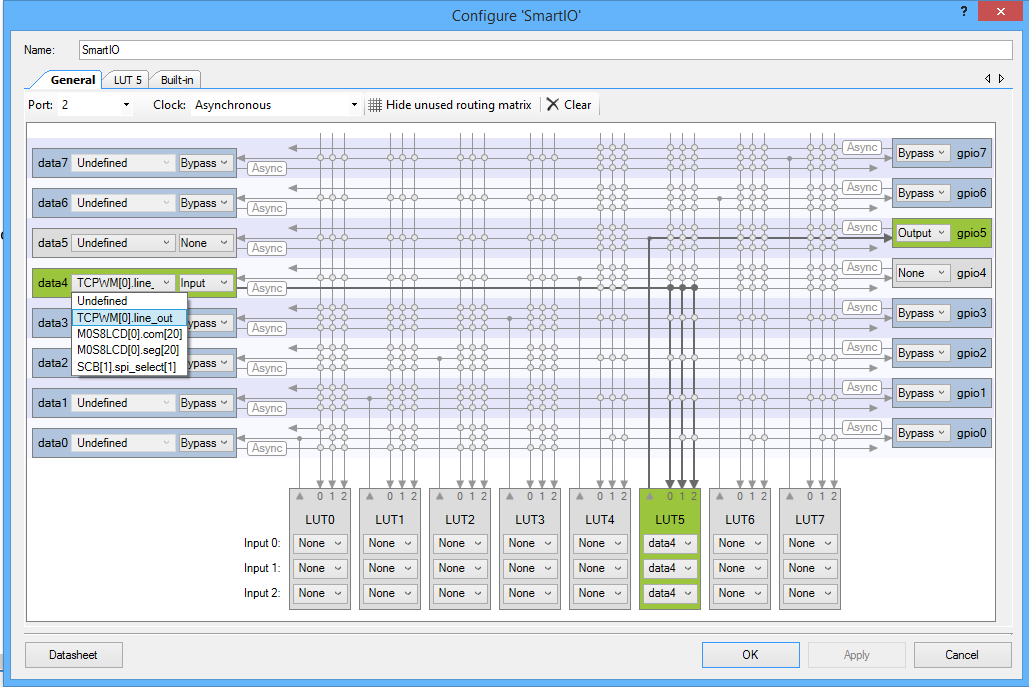
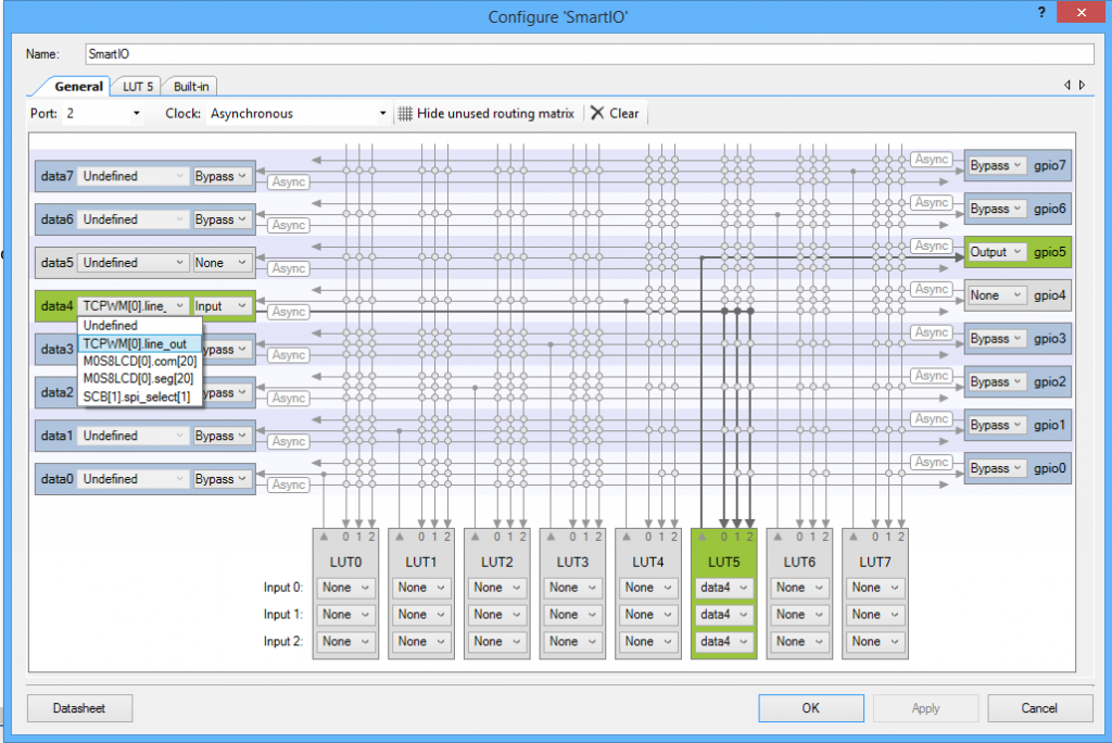
  1. Select Port 2
  2. Configure GPIO 5 to “Output”.  This can be done by either clicking on the “solder dot” or by selecting output from the drop down menu
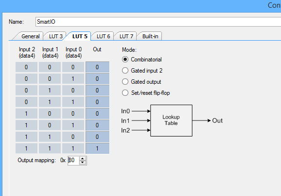
  3. Select data 4 as “Input”
  4. Select data 4 as “TCPWM[0].line.  Remember that this is ONLY for your information and doesn’t actually change anything in the project.
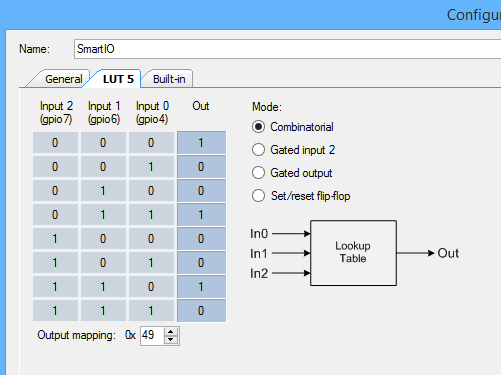
  5. Select the 3 inputs to LUT5 to be the data4 line which can be done from the three drop down menus or by clicking the three corresponding solder dots.

Screen Shot 2016-03-06 at 9.53.10 AM
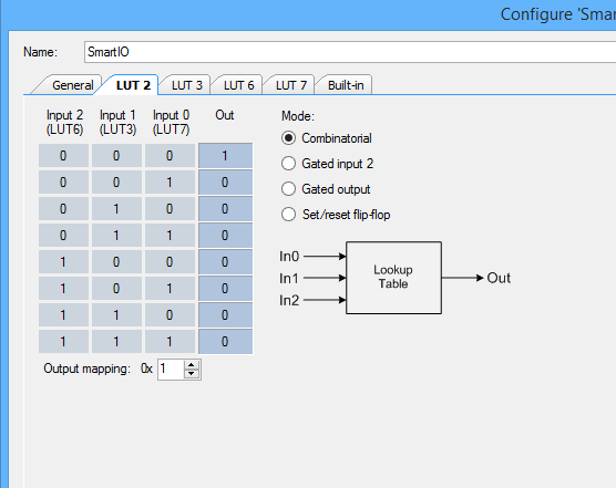
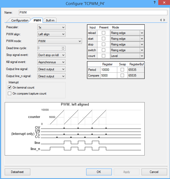
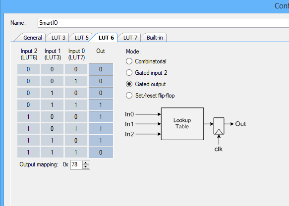
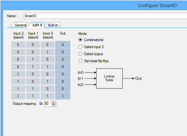
Next, I configure the LUT to “passthrough” by setting up 000 = 0 and 111=1 (which are the only two possible combinations as the three inputs are tied together).  You change the “Out”s from 0->1 and 1->0 by clicking on it.

LUT5

Then I will re-wire up the schematic to look like this:

blue-led-schematic-smartio

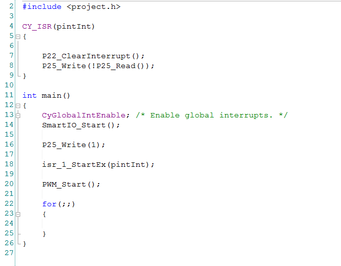
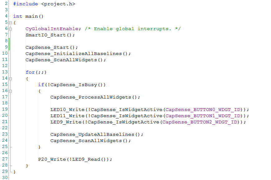
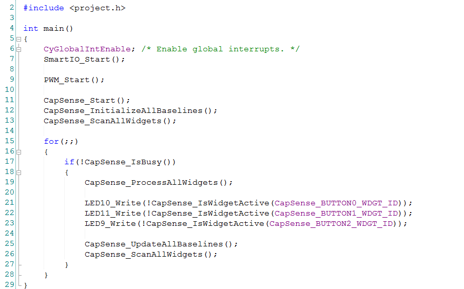
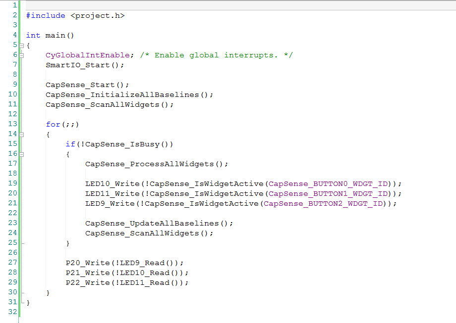
The firmware is trivial,  just start the PWM and the SmartIO

blue-led-firmware

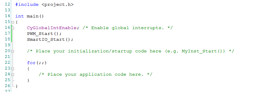
When I program the kit the blue LED starts blinking.  Cool.

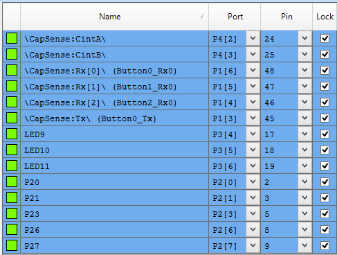
In the next posts I will teach you how to use some other configurations of the Smart IO and how to use the CapSense block to create inputs for the Smart IO.

You can find this PSoC Creator workspace on github in the directory called “SmartIO”.  This project is called “SimpleSmartIO”.

Index Description
PSoC4000s & The SmartIO – Part 1 An introduction to the SmartIO and first project
PSoC4000s & CSX Mutual CapSense Buttons Part 1 Using mutual capacitance
PSoC4000s & CSX Mutual CapSense Buttons Part 2 Using the CapSense tuner
PSoC4000s & The SmartIO – Part 2 A 3 input XOR logic gate
PSoC4000s & The SmartIO – Part 3 A 3 bit up counter state machine
PSoC4000s & The SmartIO – Part 4 Using an external clock with the Smart IO
PSoC4000s & The SmartIO – Part 5 Triggering an interrupt