Summary of Eagle PCB Layout Guidelines
I typically design my PCB’s in Eagle and have them manufactured at OSH Park. Each new PCB layout feels like I am starting nearly from scratch because I only do about 1 or 2 boards per year. Every time, as I go through the process, I promise myself that I am going to write down the list of things that I always need to relearn. But, I never seem to get the list written down. Today things change. Here is my list:
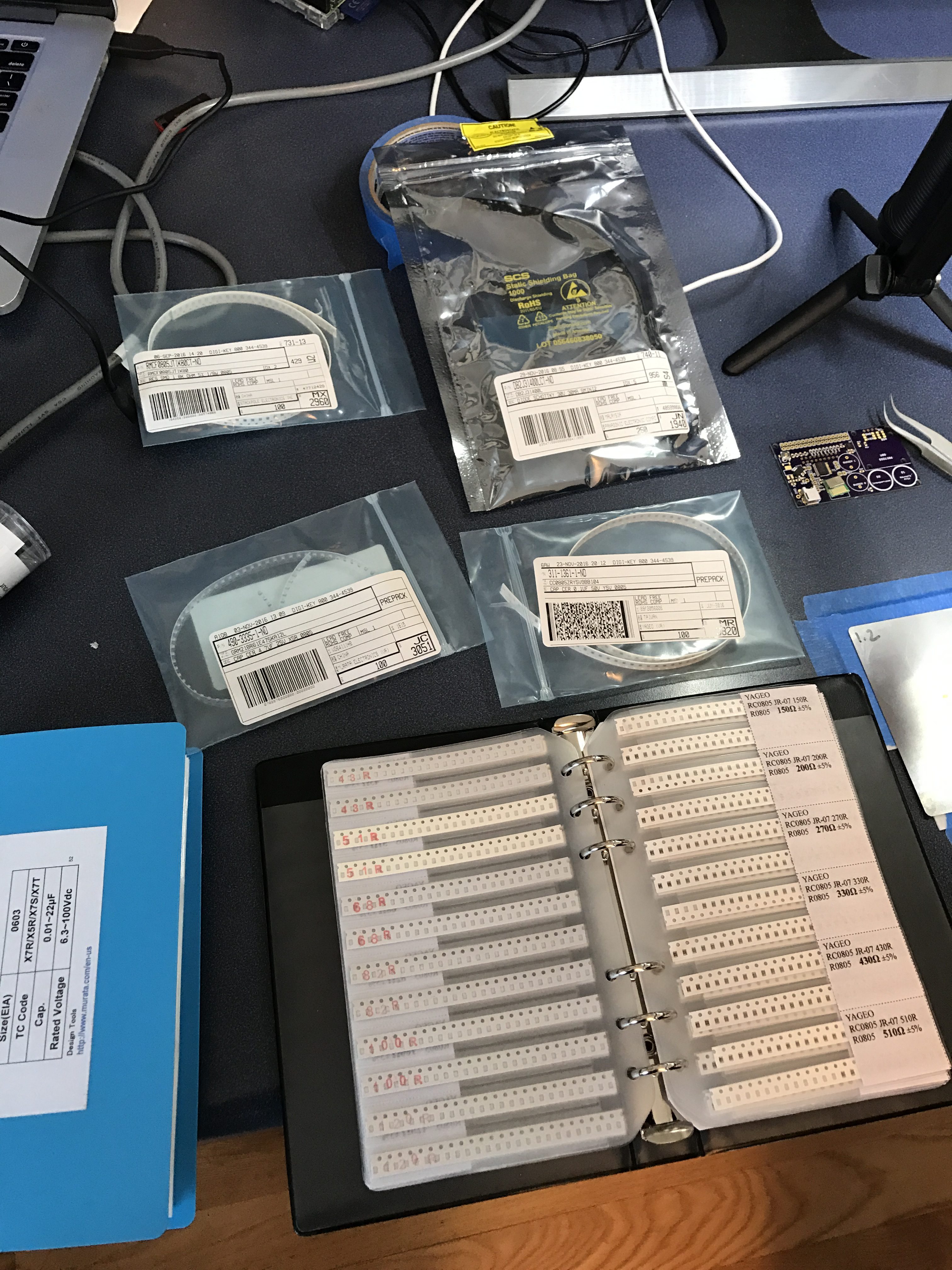
- Make sure that you can actually purchase the components you put in your design
- No Airwires
- Vias tented (or not)
- Ideally no more than 2 vias on a net
- Power nets > 40mil
- Auto router setup
- Fill on the ground plane
- Ground fill around CapSense Widgets
- Test points on key nets – at very least power and ground
- Silkscreen font size
- Silkscreen labels on key nets
- Silkscreen key information onto the board
- Put in power supply jumper
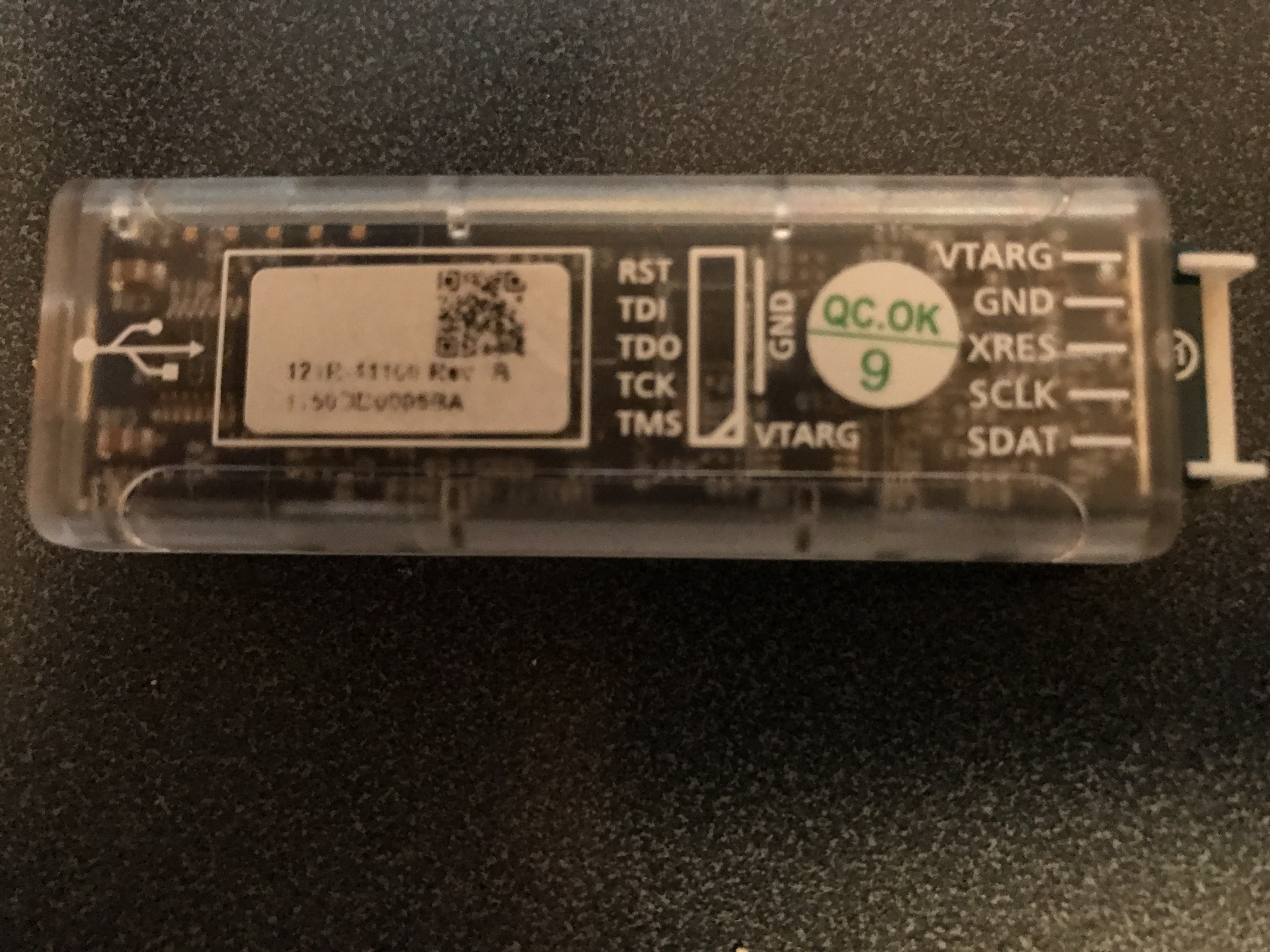
- If there is I2C then put in a blank header to connect a mini-prog-3
- Extend the QFN footprints enough to be able to rework them
- Try not to route under QFNs
- Try not to use QFN with 0.5mm pitch
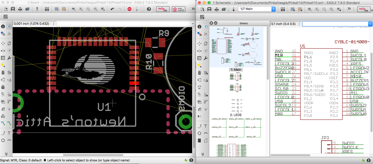
- Use the eye tool to compare every net in the schematic and layout
- DRC
- ERC
- CAM Job
- Don’t forget about the stencil
Make sure that you can actually purchase the components you put in your design
I used a footprint I found on the internet assuming that there was good availability for it. But, I ended up having to order some weird USB connectors from a salvage shop in Poland. I guess that I felt lucky to have been able to find them at all. Unfortunately, I did the whole board and sent it to the shop before I was sure that I could buy everything. Always always check to make sure you can purchase the device you place on the board.
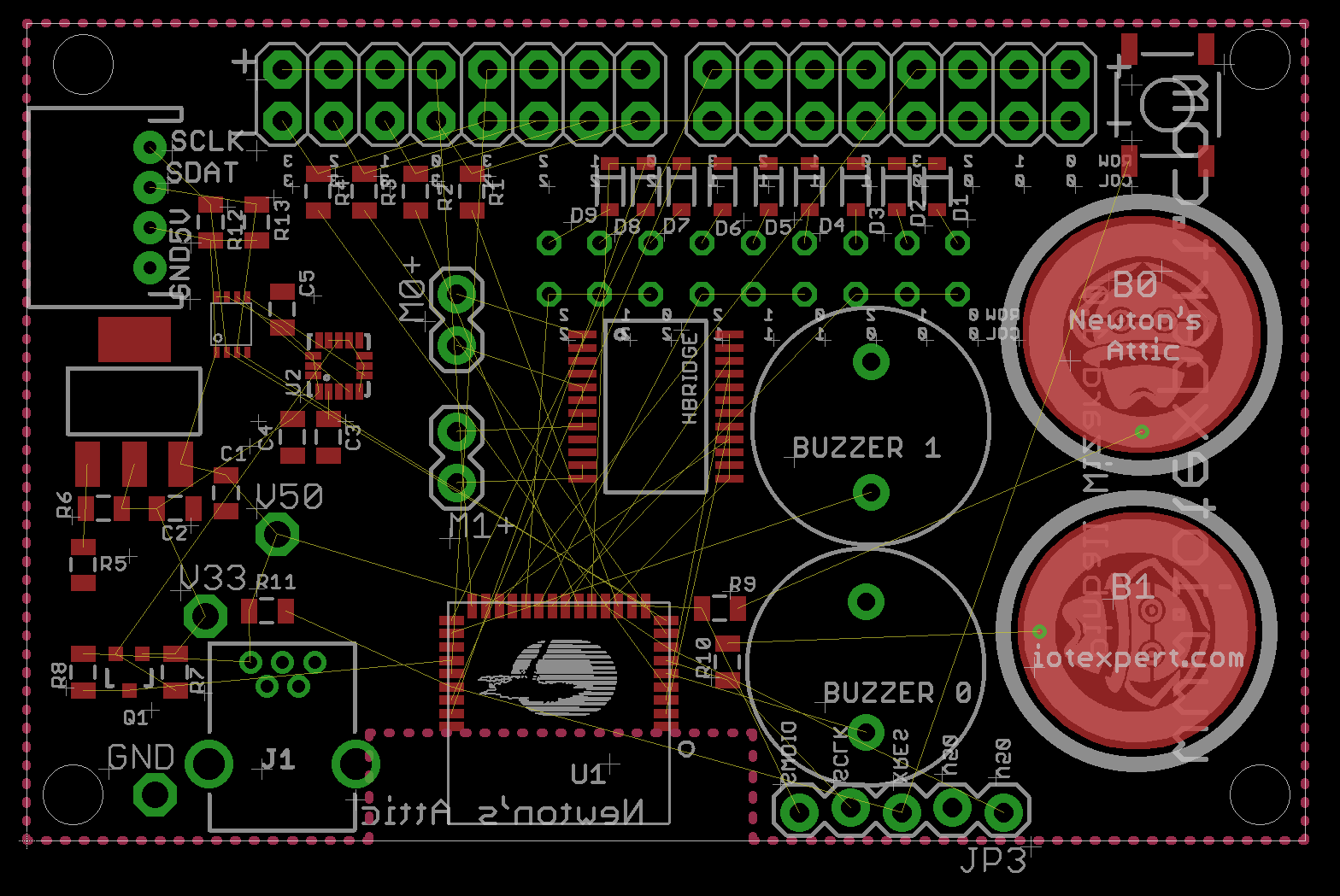
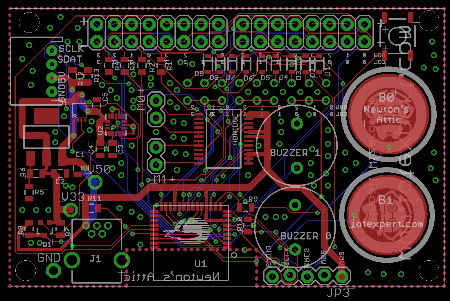
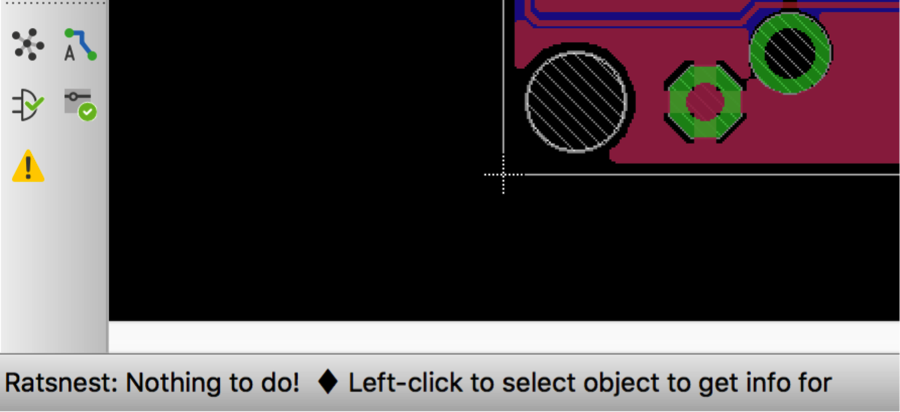
No Airwires (seems like it would be obvious… but)
Airwires show the connectivity that is drawn in the schematic. Unfortunately they don’t conduct electricity. Until a REAL connection is made you will have a yellow flight line connecting between the pins in your layout. Before you tapeout the board you MUST MUST press the Ratsnest button and get the message “Ratsnest: Nothing to do!”
If you do this:
Then you will need this:
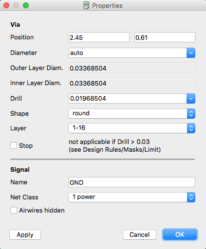
Vias tented (or not)
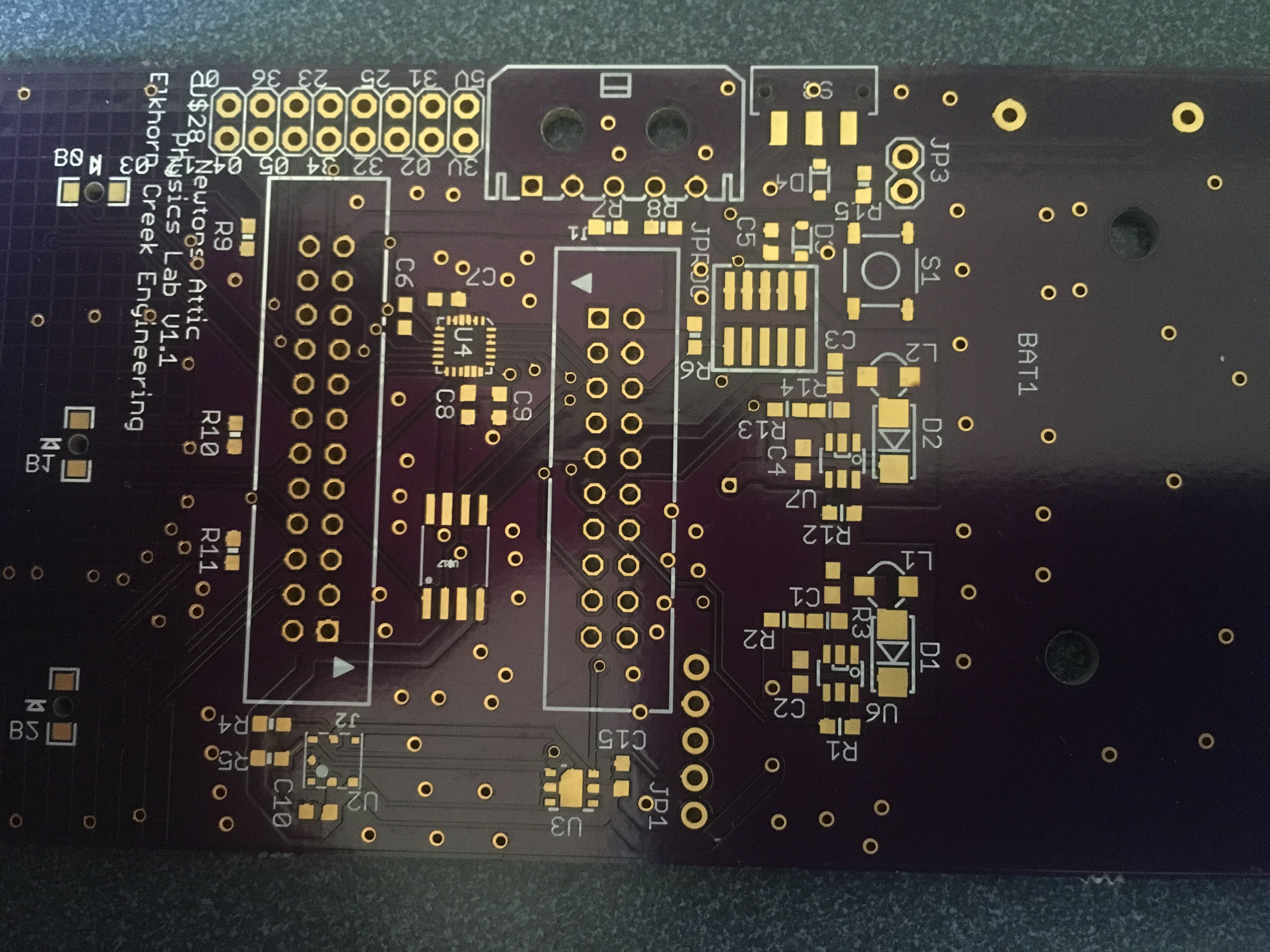
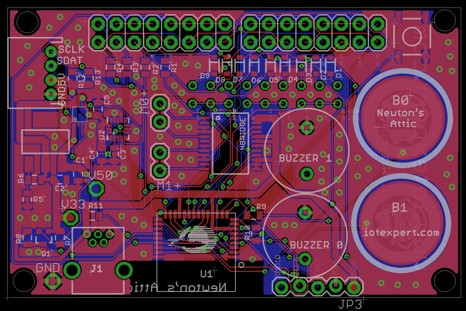
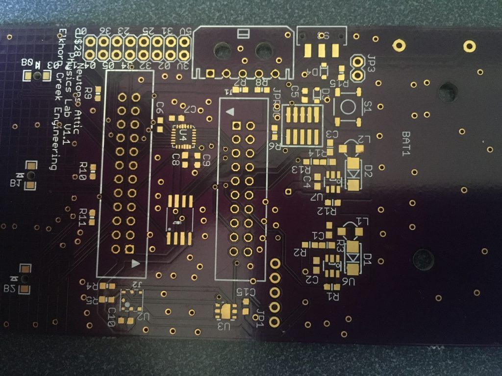
A tented via or a plugged via is a connection between the top and bottom of the printed circuit board that is covered with solder mask. In general there are probably enough vias on your board that if you don’t cover them you will not be able to see the silkscreen (either because it won’t print on copper or because the PCB vendor will trim it). Here is a picture of one of the versions of Physics Lab where I forgot to tent the vias. In the upper left where it says “Elkhorn Creek Engineering” you can see that the “l” in Elkhorn and the “g” in Engineering is partially missing where there is a via in the board.
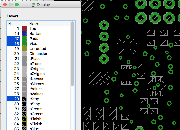
In Eagle PCB, Vias (and Pads) are automatically covered with the “tStop” mask. Here is a screen shot of a PCB that I am working on with just the “Pads”, “Vias” and “tStop” layers shown. You can see the “big” holes which are Pads for through-hole components. You can see that they have the diagonal white lines through them that represents the “tStop” mask. tStop is the mask that prevents the solder mask from being applied. In the picture you can also see the tStop on places where there are SMD pads. And, you can see a bunch of the smaller vias which are not covered.
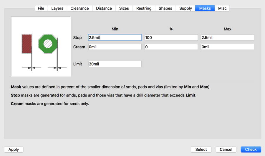
To tell Eagle PCB to turn off the tStop for vias you need to change the design rules on the “Tools->DRC->Masks” screen. The limit parameter tells Eagle PCB to NOT create “tStop” for any via/pad that is less than 30mil in diameter.
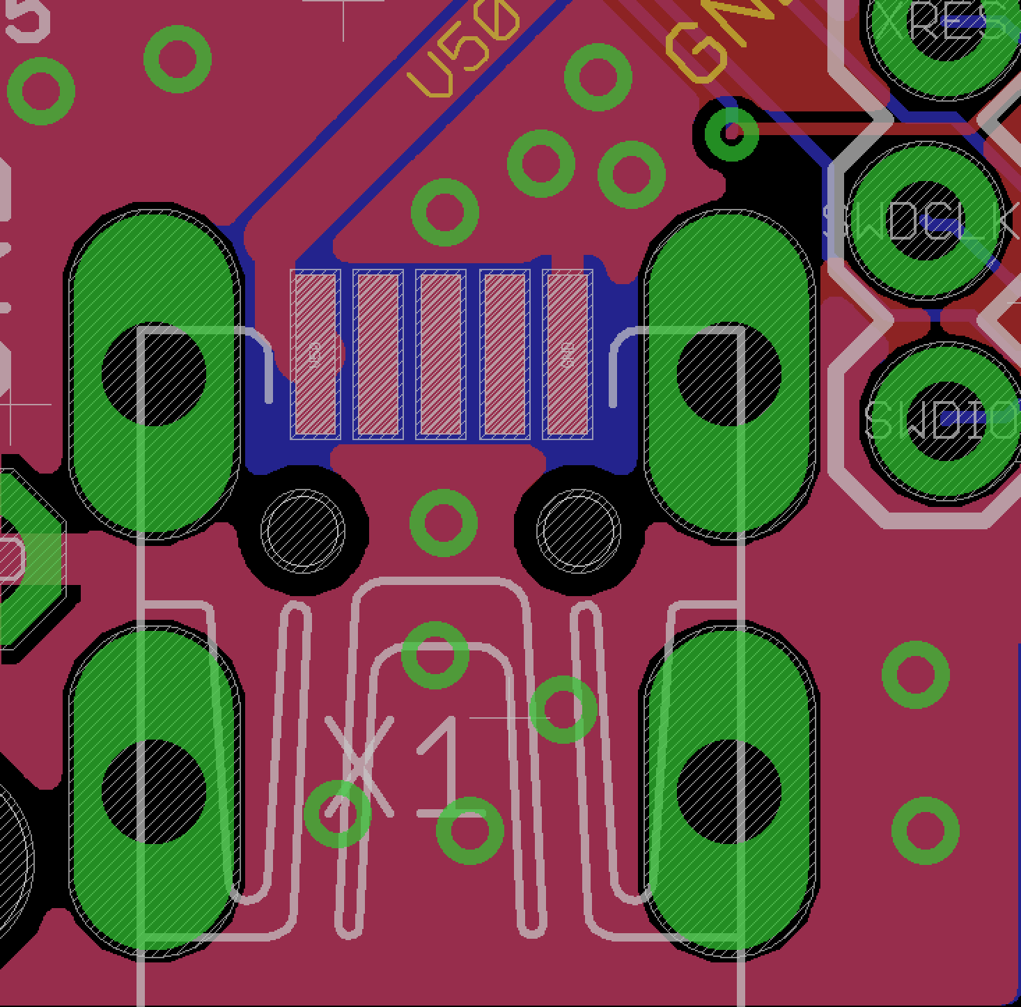
No more than 2 vias on a net
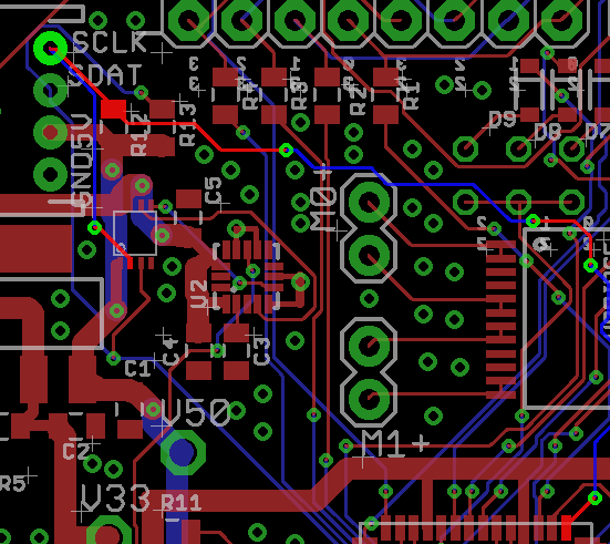
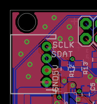
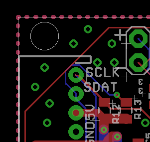
I always strive to keep all of the nets on my two layer print circuit boards to have no more than 2 vias. To look for this I click on the “eye” tool to probe each net of the layout, then I manually trace the net. Here is a screen shot of a net that I try to avoid. You can see that the net starts on the SMD pad in the lower right, then winds its way to the top left. It goes through 4 vias. Unfortunately it goes through one more via before reaching the SMD pad just below the upper left.
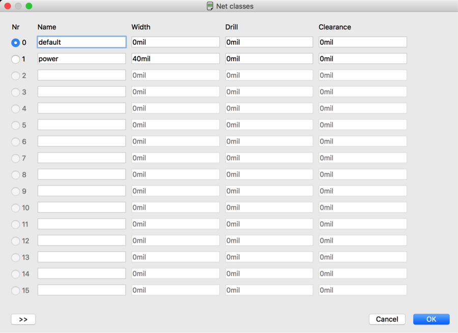
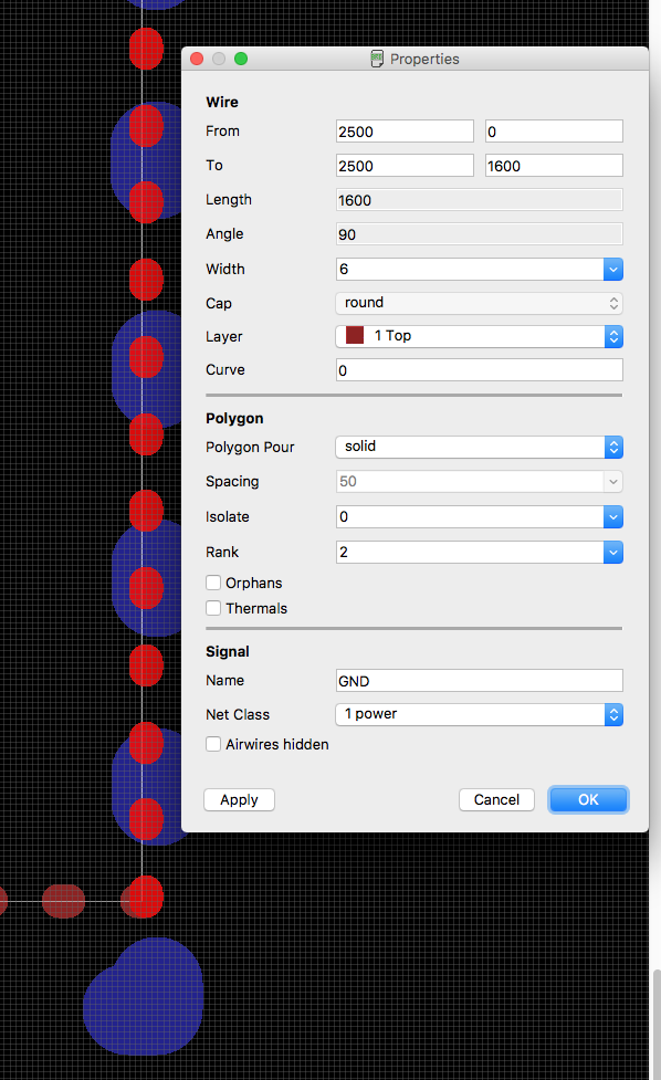
Power nets > 40mil
I like the power and ground nets to be routed in at least 40mil wires. To do this, you first need to create another net class in the “Edit–>Net classes” menu. I always create a class called “power”. Then I set the minimum width to 40mil. If for some reason you want to have a minimum clearance or drill you can set this here as well. If you leave it at 0, Eagle PCB will use the default rules.
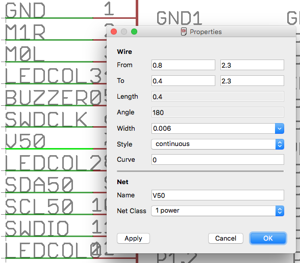
After you have created the power net class, you then need to assign the correct nets to the net class. You do this in the schematic by selecting the “I” tool, then clicking on the net. Then you can select the “Net Class” for that net. In this case I am editing the V50 net.
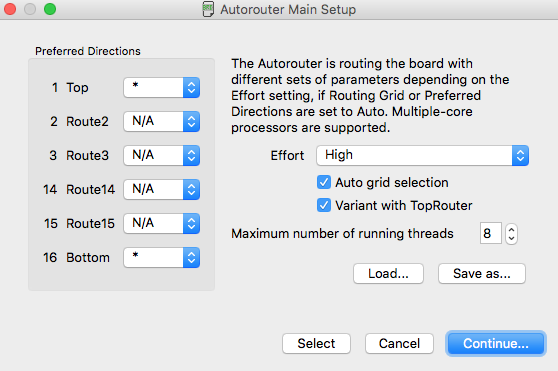
Auto Router Setup
I am absolutely terrible at designing PCBs. This frustrates me to no end. One of the crutches that I like to use the the Eagle PCB Autorouter. The only change that I currently make is to use the “*” option to let the router go whatever direction it thinks that it should.
Fill on the ground plane
To create a ground plan you need to:
- Draw a “polygon” around your board in the “top and bottom” layers.
- Attach those polygons to the correct net e.g. “gnd” by typing the “name” command and then clicking on the ground polygon
When you press the “ratsnest” button Eagle will fill the ground plane.
If you want it to unpour it you can run “ripup @;”. When the ground plane is not filled it will appear as a dotted line around the board:
To attach the top and the bottom ground planes together you need to put a via on the correct net. To do this:
- Click on the “via”
- Click where you want it to attach the top and bottom
- Add to the the right net using the “name” command and then typing the signal name
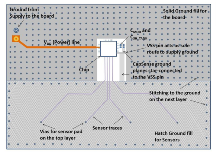
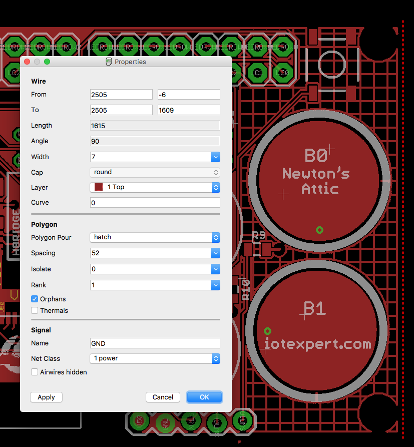
Ground Fill Around CapSense Widgets
In order to get the best CapSense performance you want to have a “hatched” ground plane surrounding your widgets. The methods for doing this are documented in the CapSense Design Guideline Section 6.4.9 “Ground Plane”. Here is an idealized view of the back of the front and back of the board:
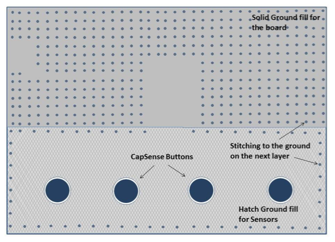
The guidelines go on to recommend that you use 25% (7 width 45 spacing) coverage on the top and 17% (7 width 70 spacing) on the back. To do this in Eagle PCB you draw a normal polygon on the top and bottom. Then you use the name command to give it the “ground” name. Then you click the “i” to set the parameters.
- Set the width to 7 (mil)
- Set the polygon pour to “hatch”
- Set the Spacing to 52 (mil). The only trick is that the Eagle PCB spacing isn’t actually the spacing between the lines but the Pitch between the hatched cells. So to achieve 45 mil spacing with a 7mil line you need 45+7=52 “spacing”
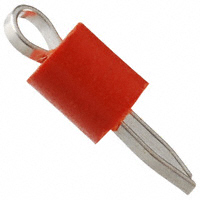
Test points on key nets – at very least power and ground
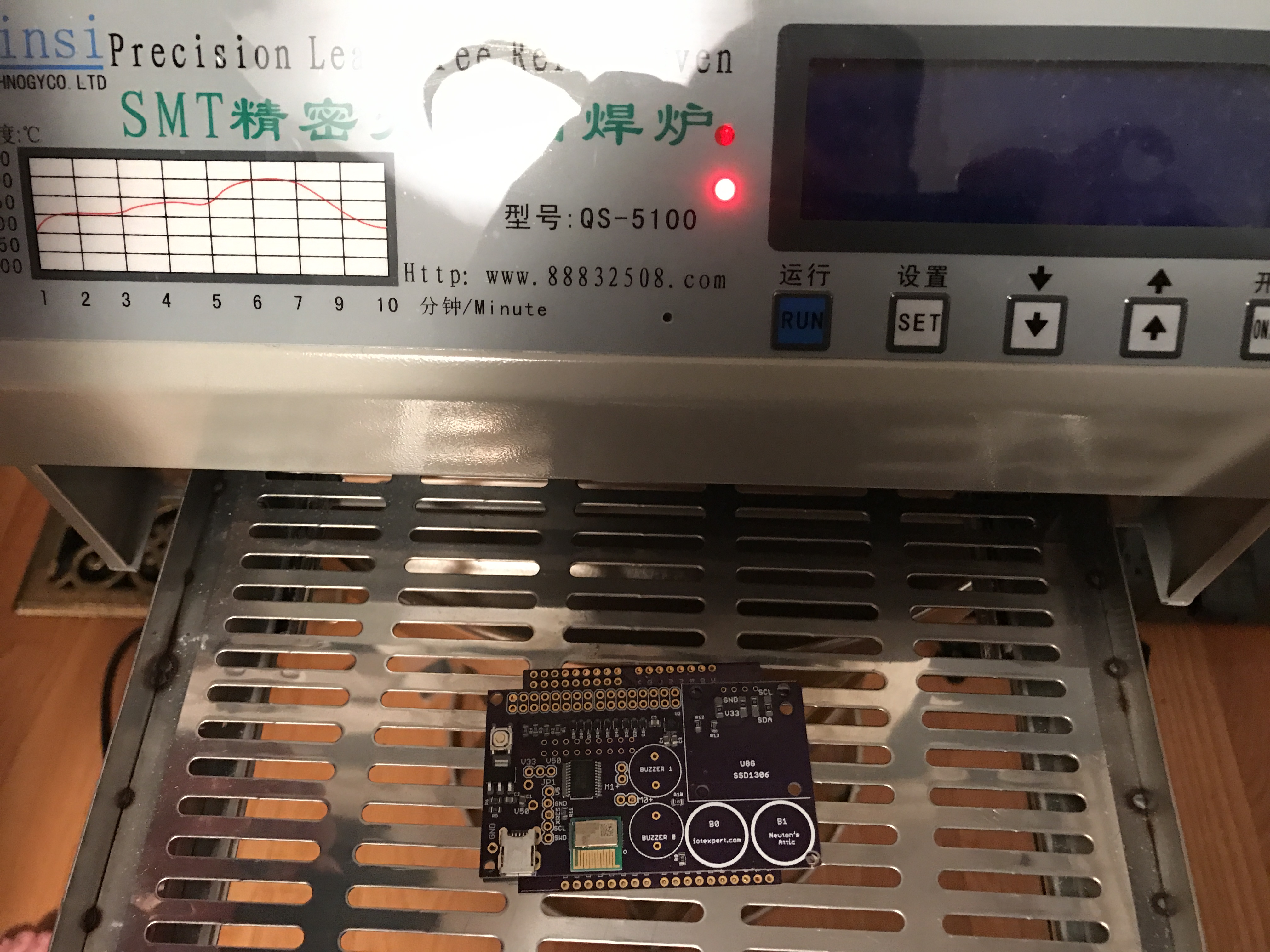
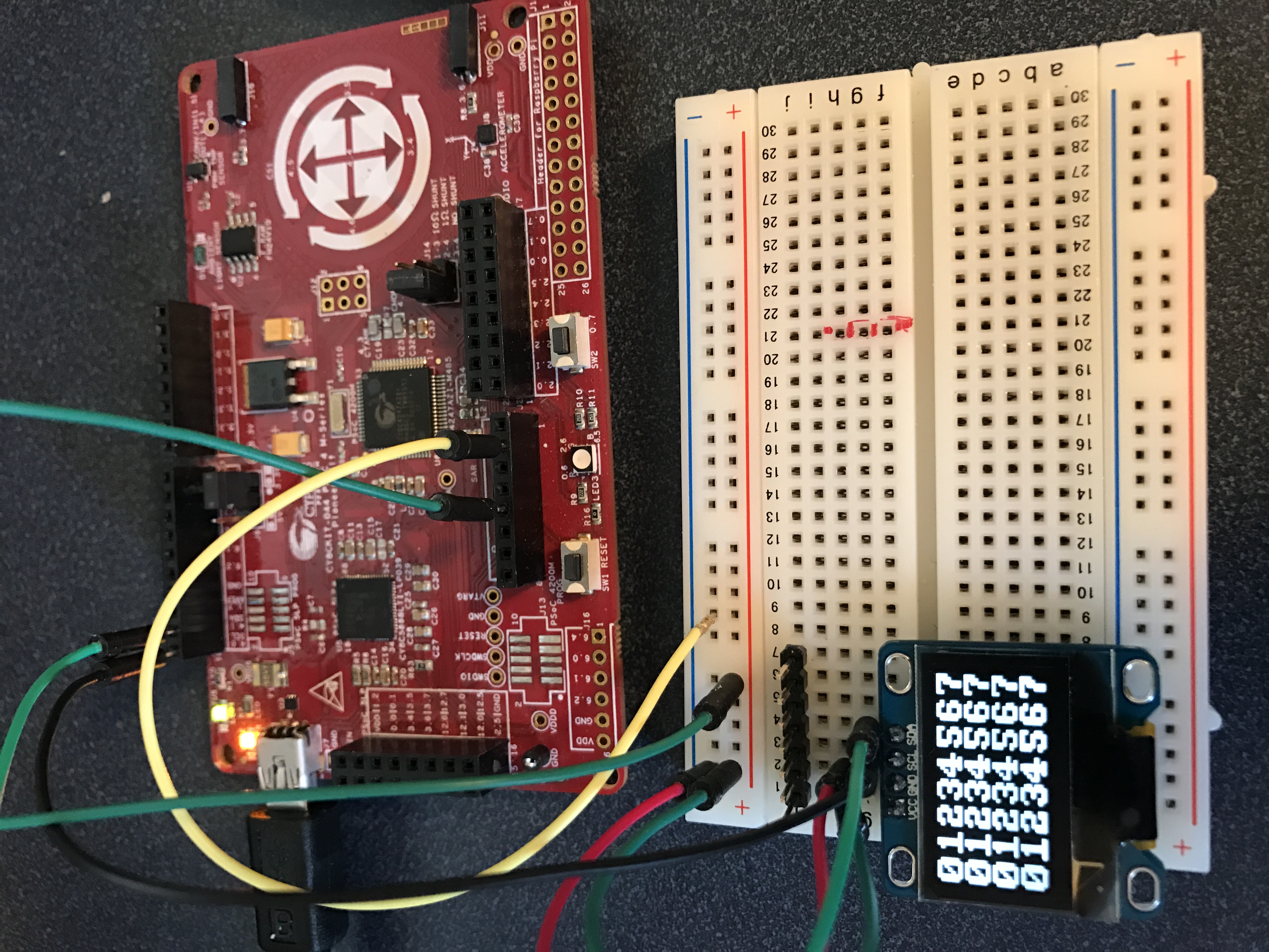
It is a serious PITA to debug a board if there is no place to attach test leads. I like to use a looped wire that you can install onto the board through a PAD. Here is a red one that I use on power nets that I bought from digikey.com
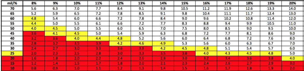
Silkscreen Font Size (don’t go less than 30mil@15%)
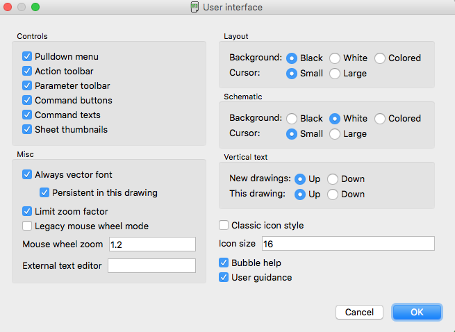
I believe that the best practice for your silkscreen fonts is to first tell Eagle PCB to use “Always vector font” on the “Options–>User Interface” menu. This will make what you see on the board much closer to what you see on the screen.
There are two issues with font size.
- First, what can you see (Im 48… so my fine vision is going away) so I think 30mil is the absolute minimum. 40mil or 50mil is even better.
- Second, what your PCB design house can print (about 5mil at OSH Park)
I am having my current PCB made at www.oshpark.com. I could not find their silkscreen spec on their website… but an OSH Park Person “tweeted” that they can print 5mil silkscreen.
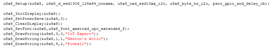
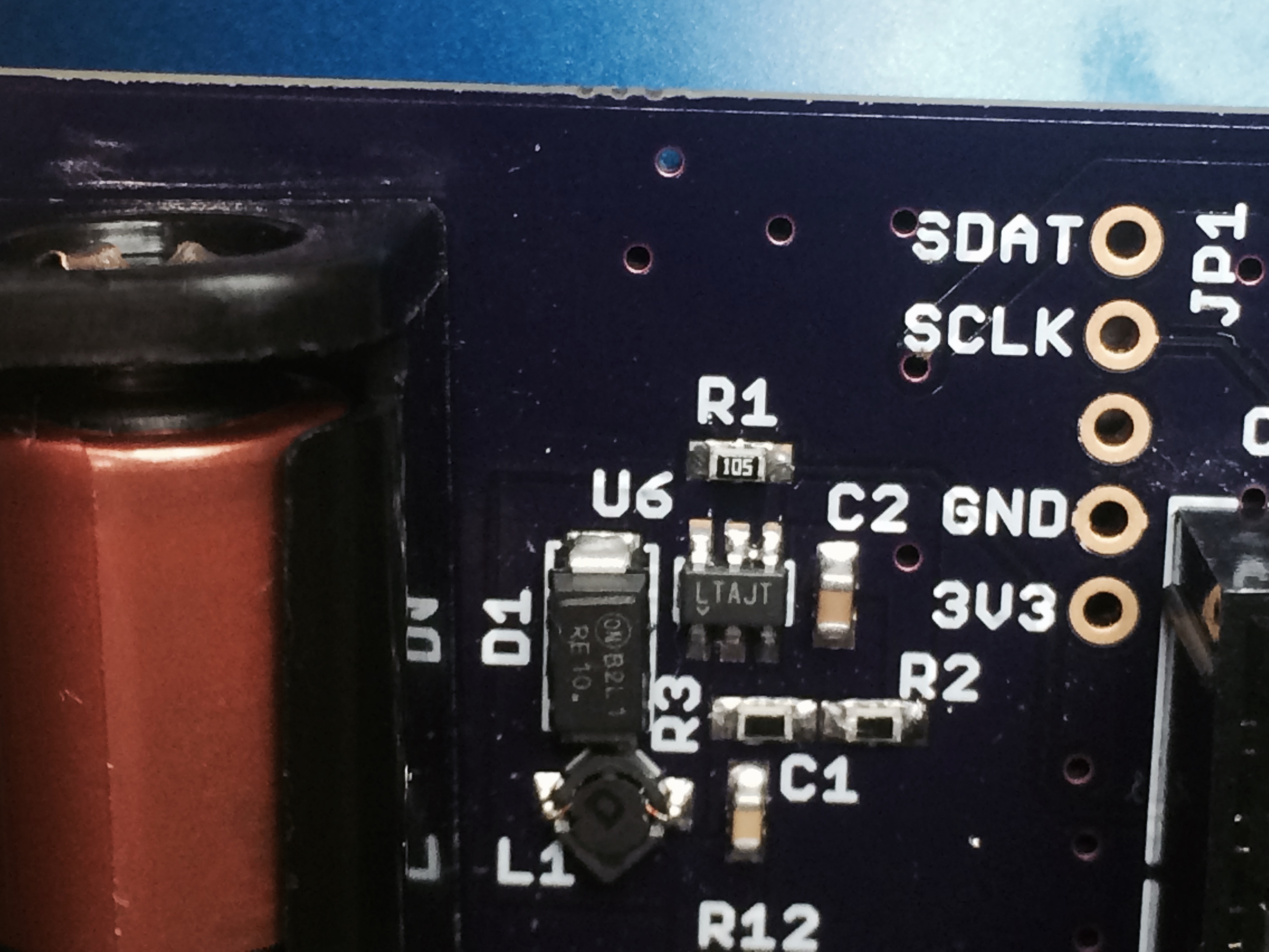
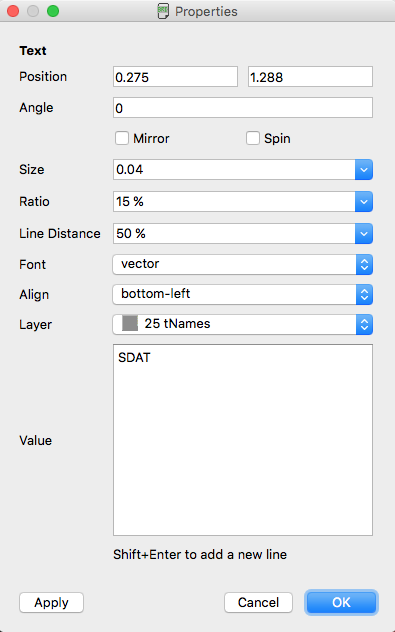
Given all of that. Your best bet is to use a “vector font”. When you select a vector font, you specify how tall the characters are, and how thick the lines are as a % of the height. Here is a screenshot of my “SDAT” label.
I made this table of what I think is a safe range:
On the the lukemiller.org blog I found a picture of an OSH park board with some different vector combinations:
On the justgeek.de blog I found another board:

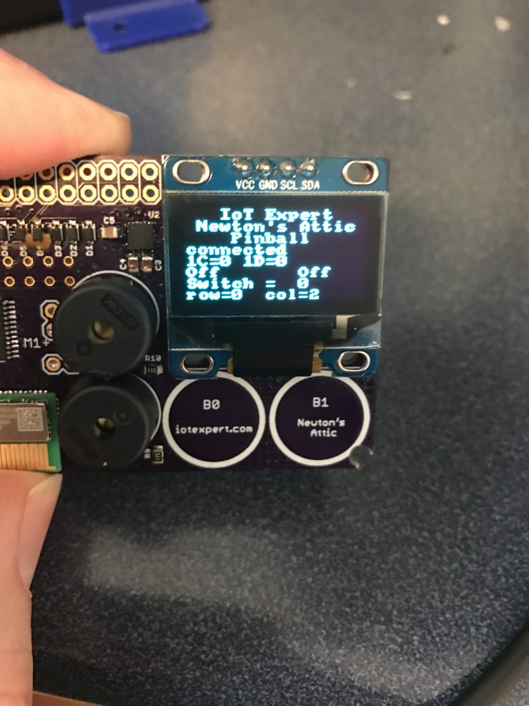
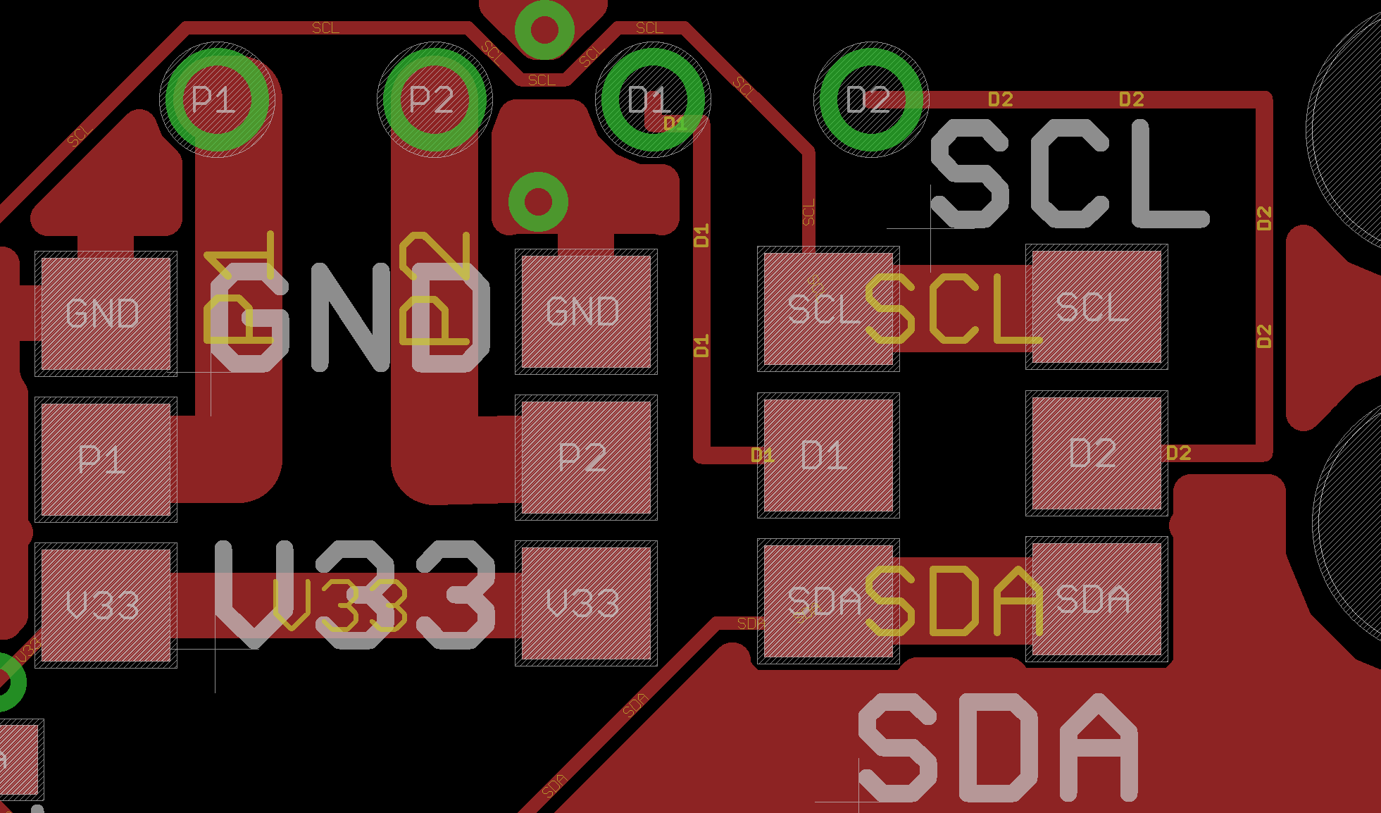
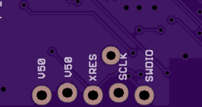
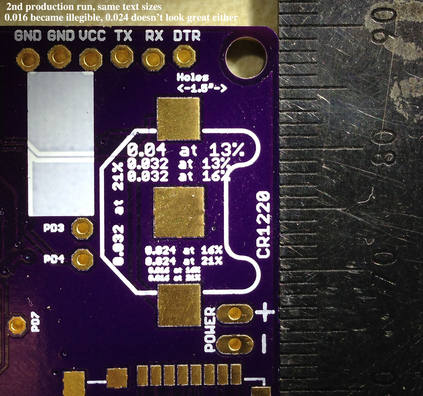
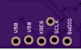
Silkscreen on key nets
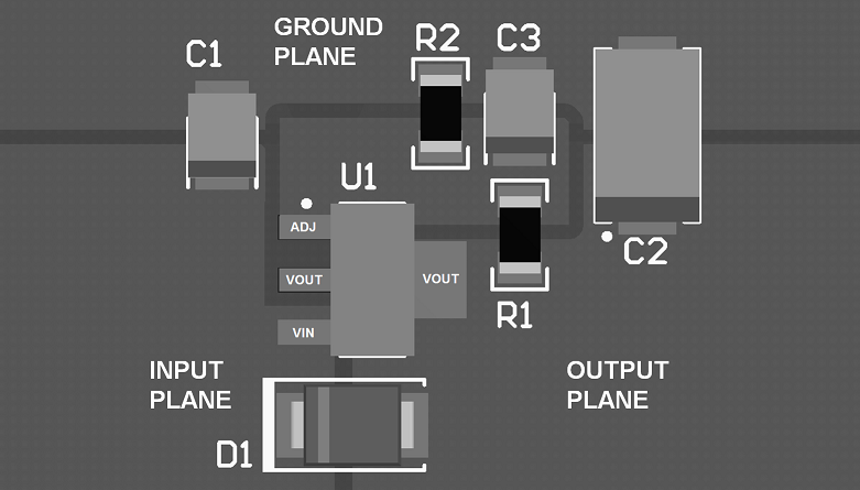
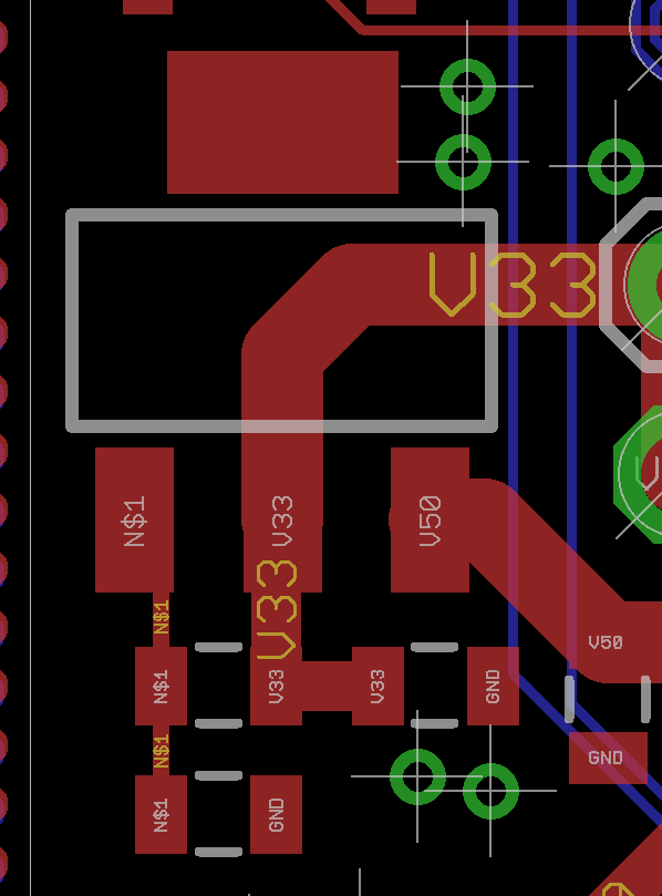
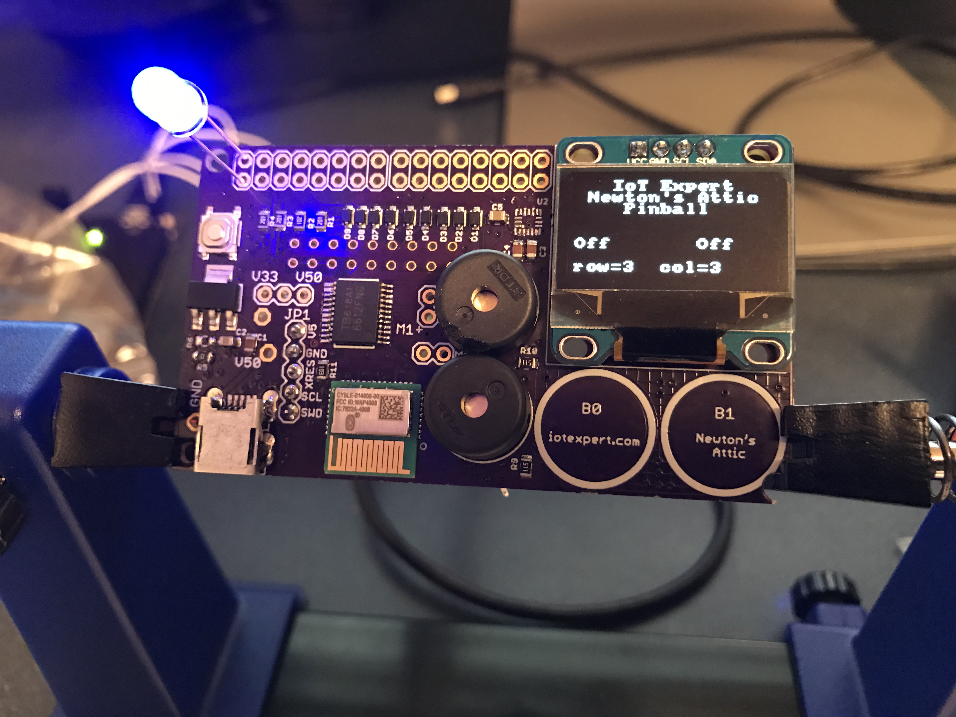
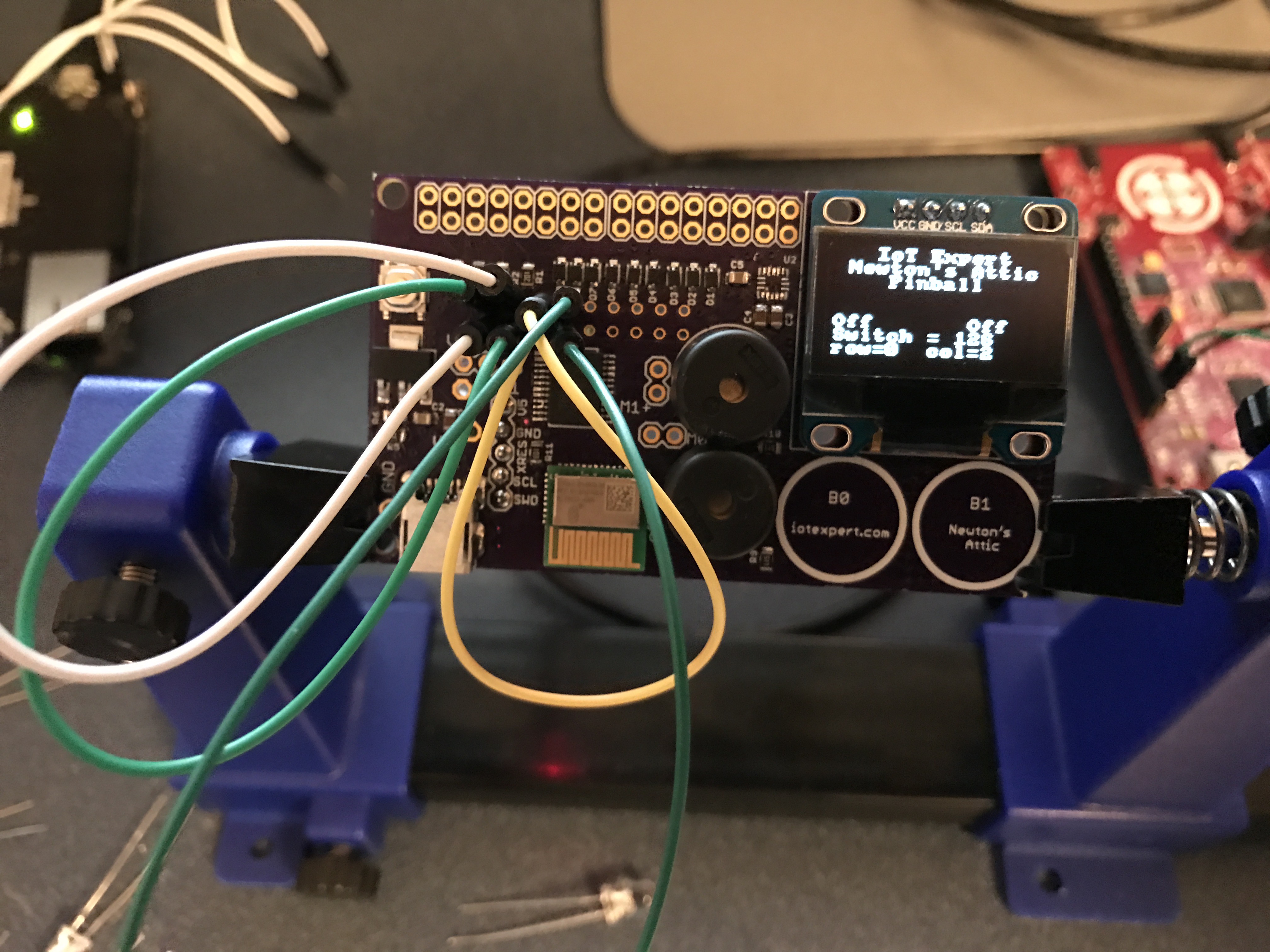
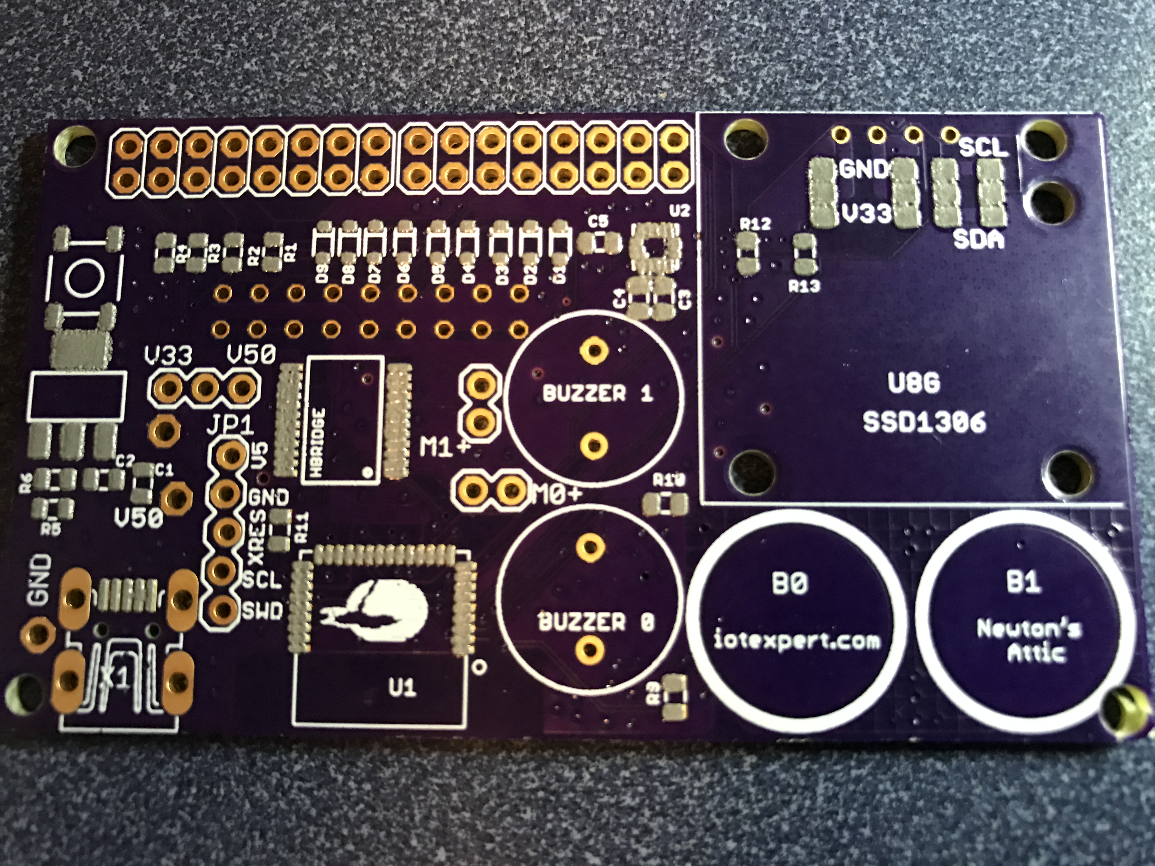
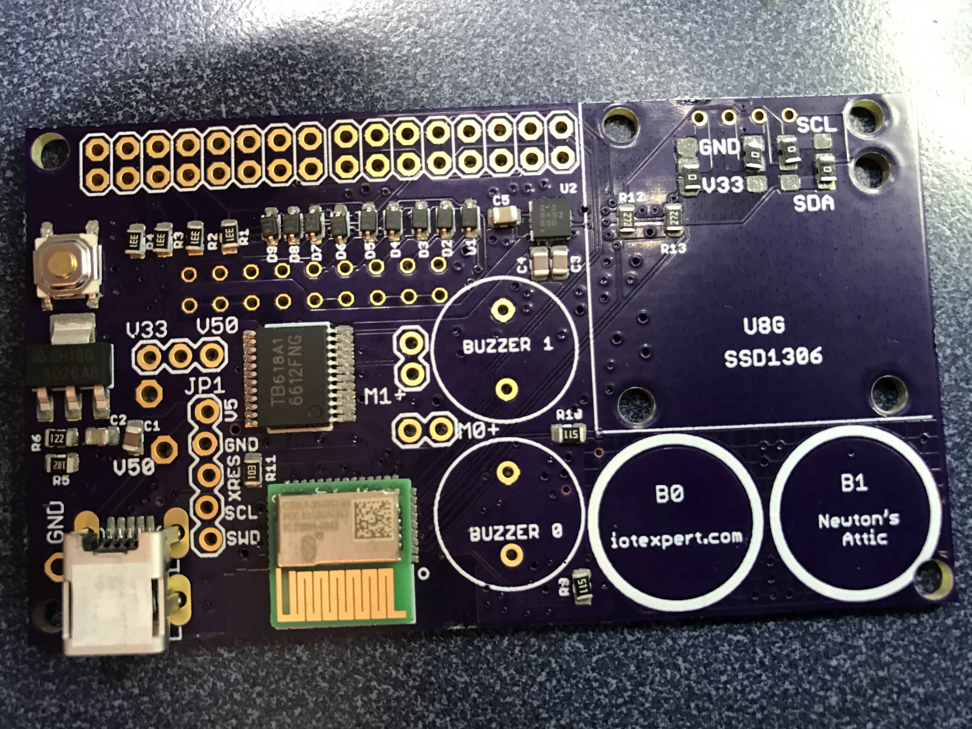
You should make sure and label every pin that you would need to interact with or debug. For example, the board below has a place to plug in a miniprog-3 in 5-pin mode: The connection is directional so labeling the pins is key: [Note: A friend of mine noticed that I labeled the MiniProg-3 connection INCORRECTLY!!!! notice that there are two V50 (when in reality the inboard one is supposed to be ground]
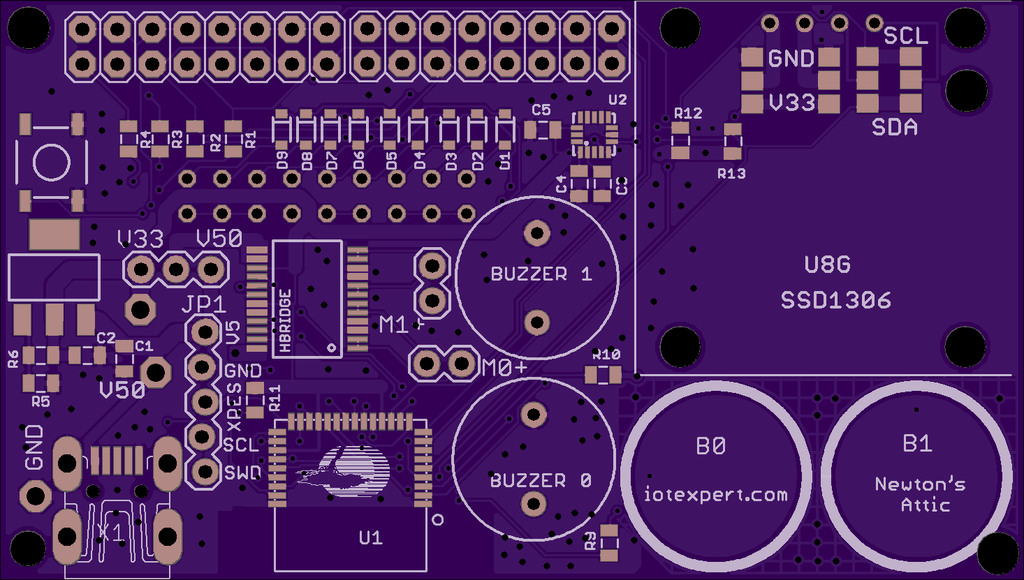
Don’t forget about the back of the board. If you don’t put labels on the back, you will endup trying to figure out what the holes are (like the ones in the lower right) by flipping the board back and forth.
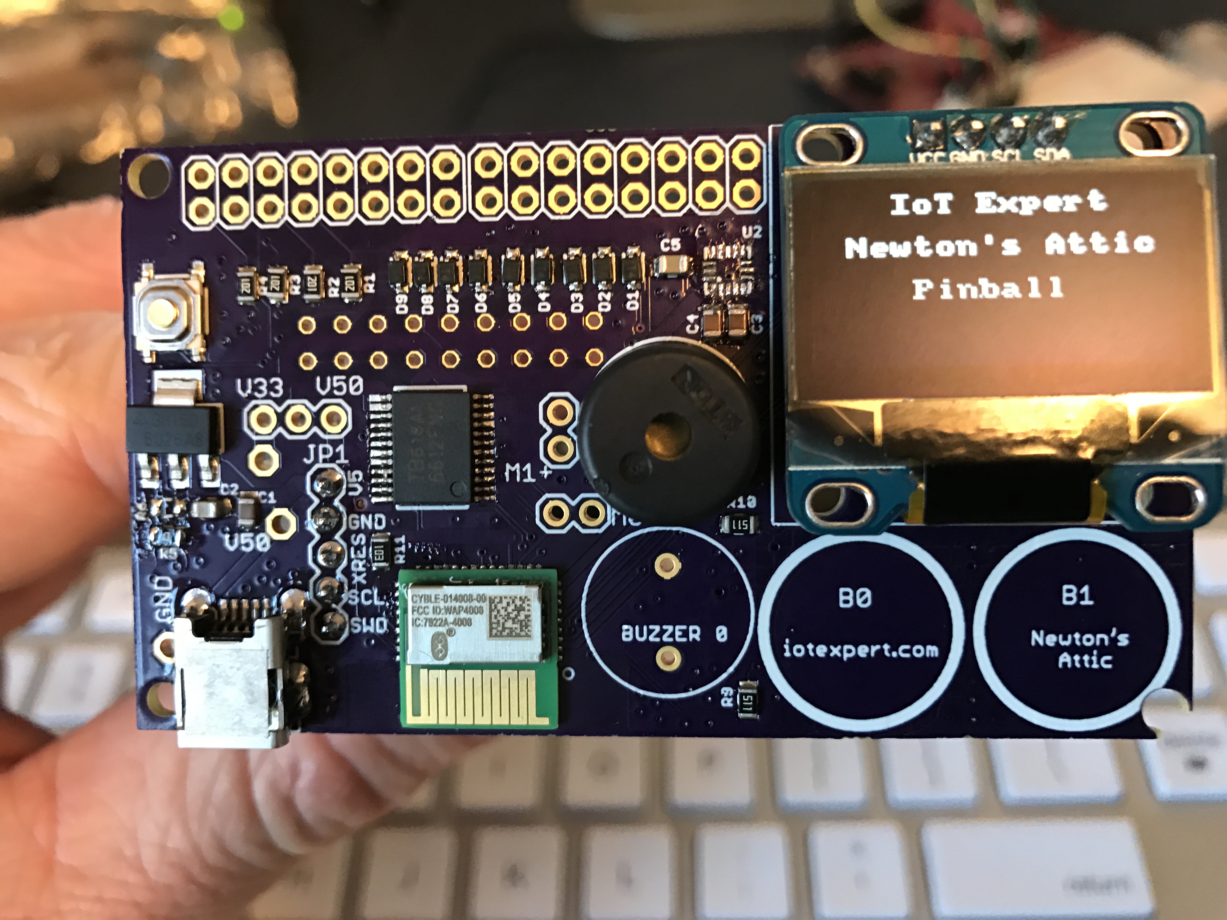
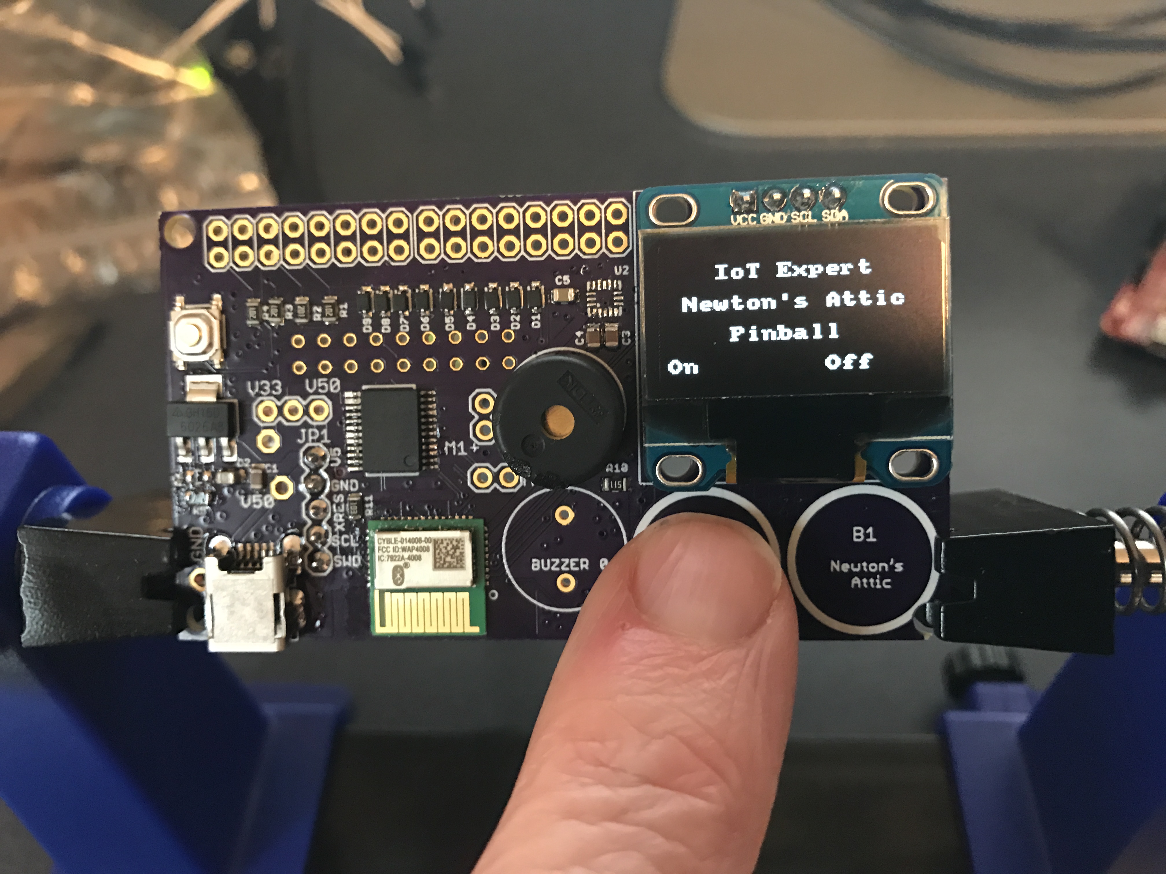
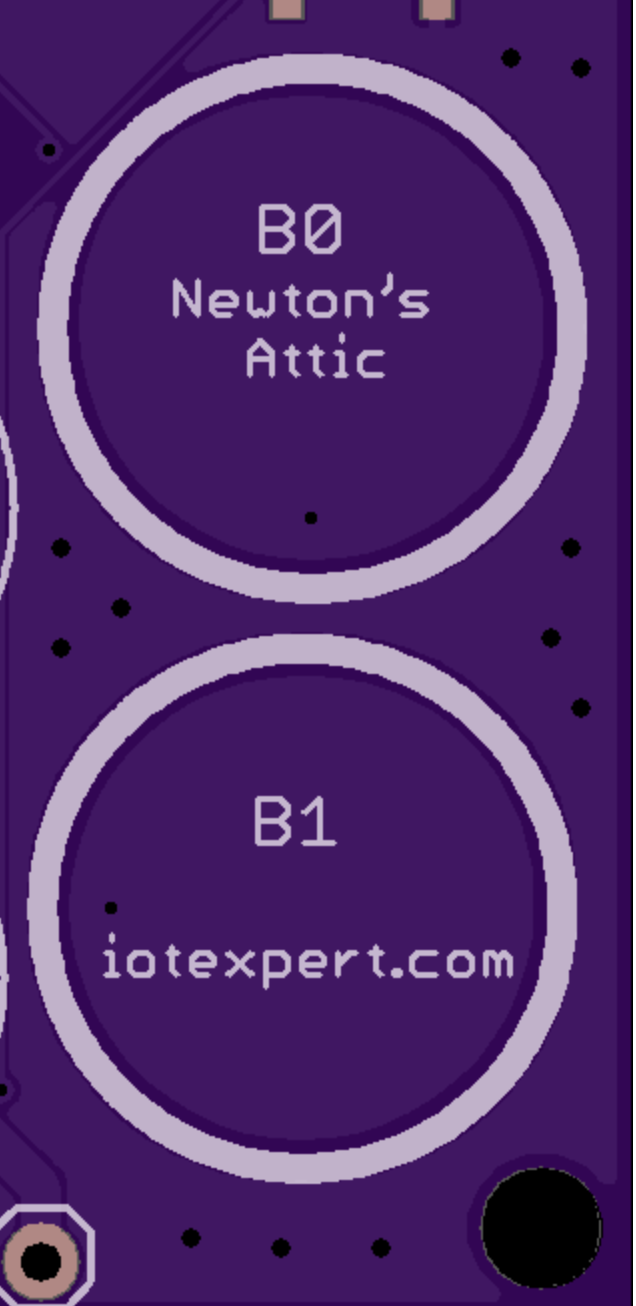
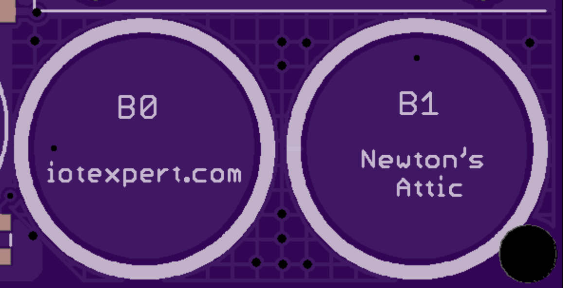
Silkscreen key information onto the board
You should definitely “comment” your board on the silkscreen with at very least:
- Name of the board
- Version number of the board
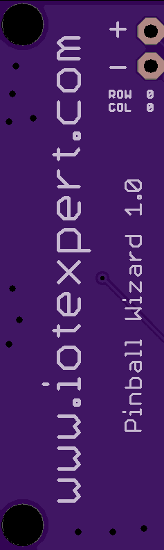
- Name of the maker e.g. www.iotexpert.com

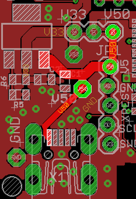
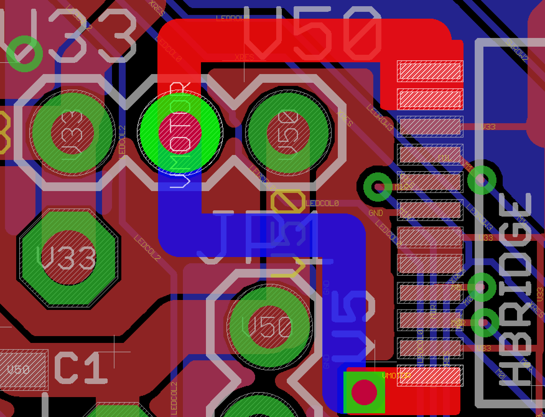
Put on Power Jumper
You should also put in a 2x100mil spaced jumpers with a 0 ohm resistor shorting them in the path of the power so that you can measure the power supply current.
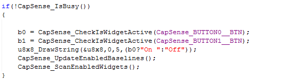
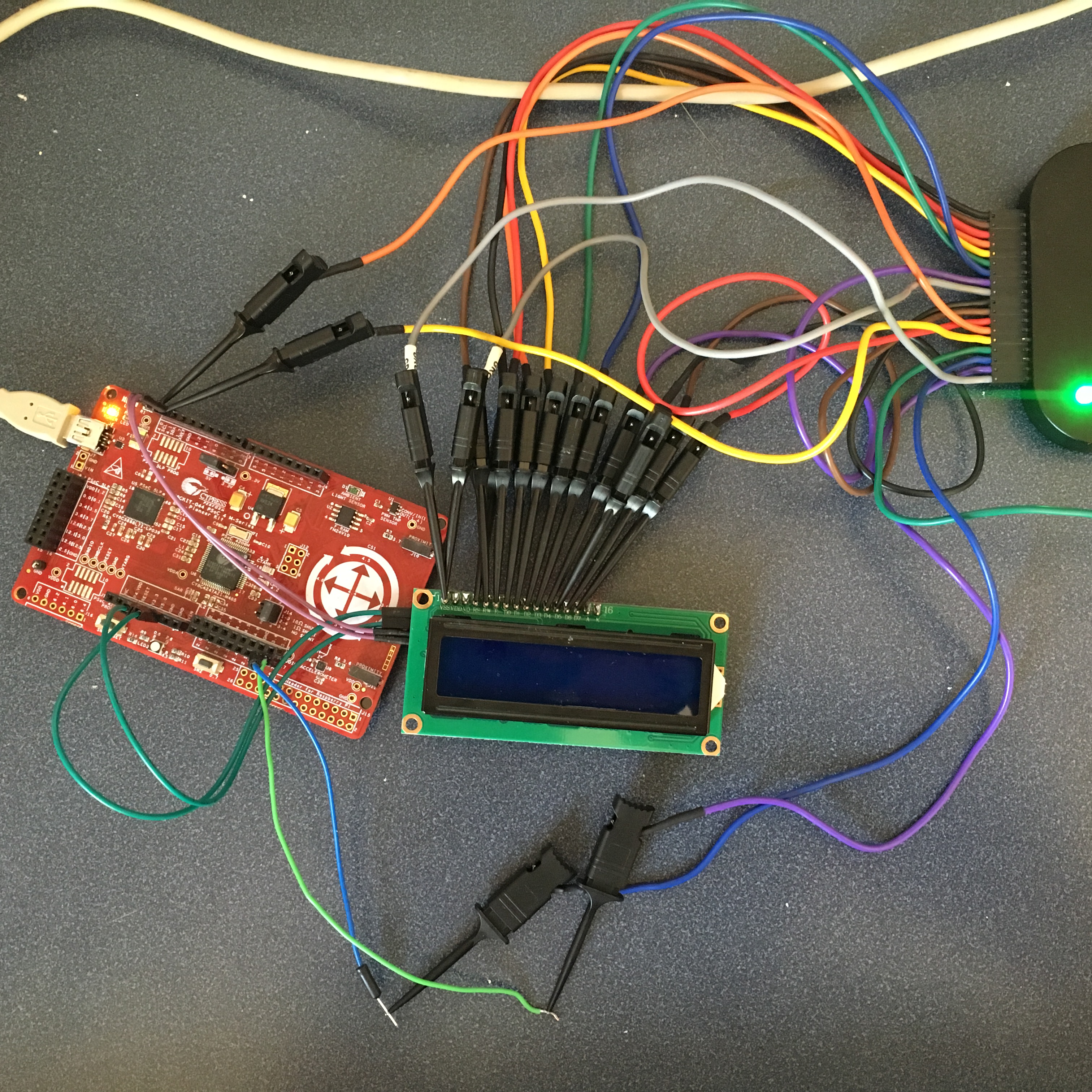
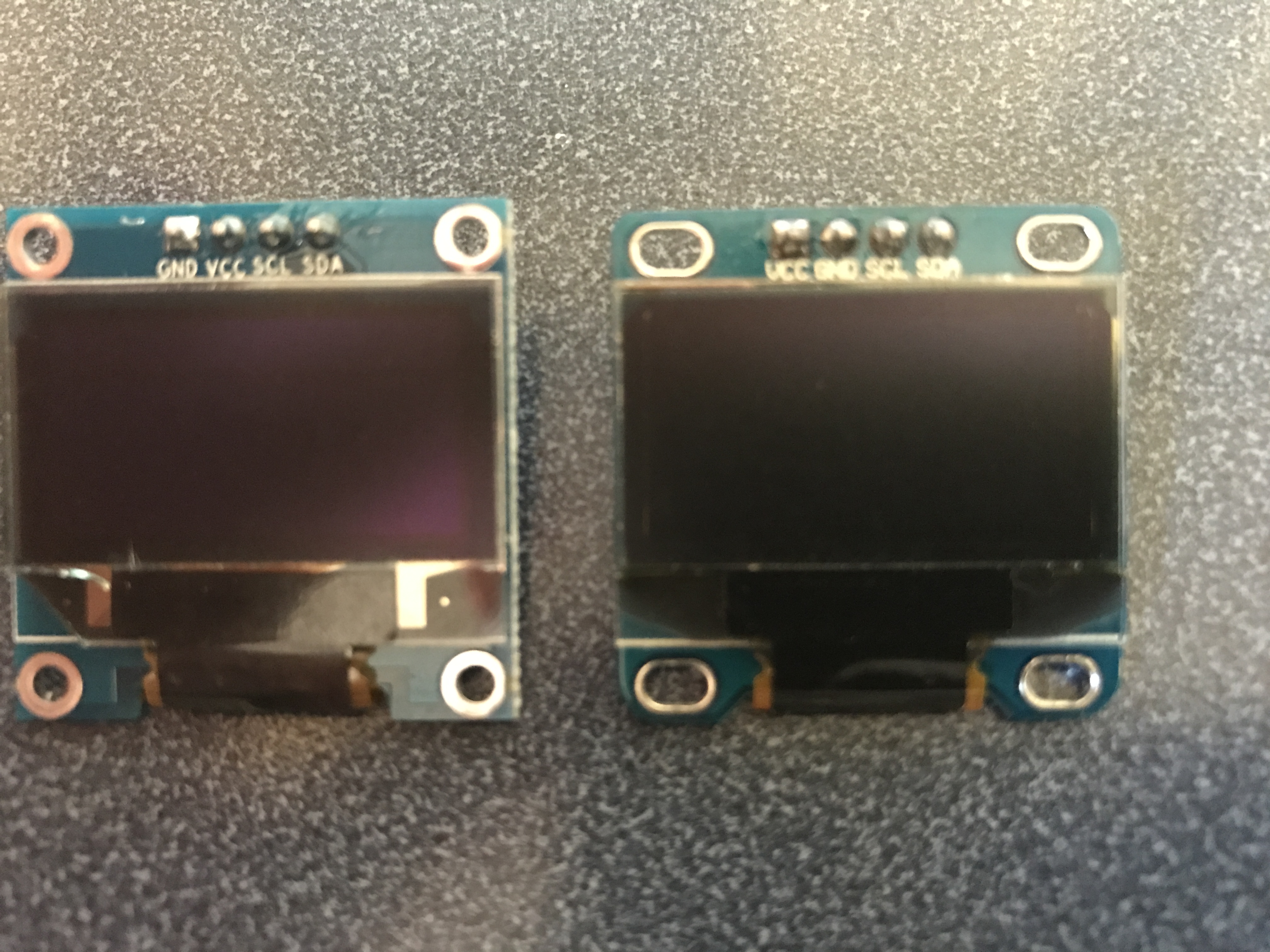
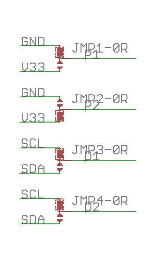
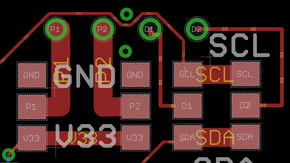
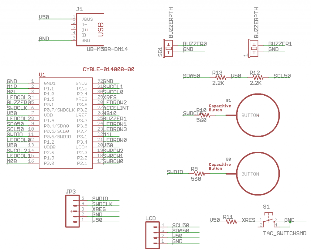
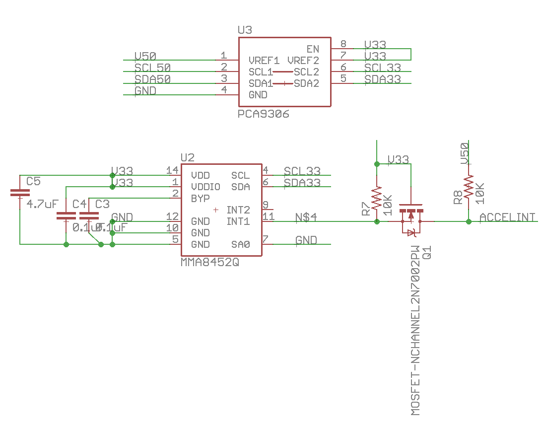
If there is I2C then put in a blank header to connect a mini-prog-3
If you have an I2C bus in your design, and you have room on the board, you should provide a place to plug in the 5-pin mini-prog3 to help you debug. This will let you interact with chips on the bus without having completed the firmware for the central MCU.
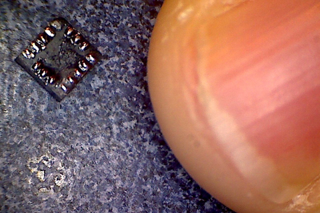
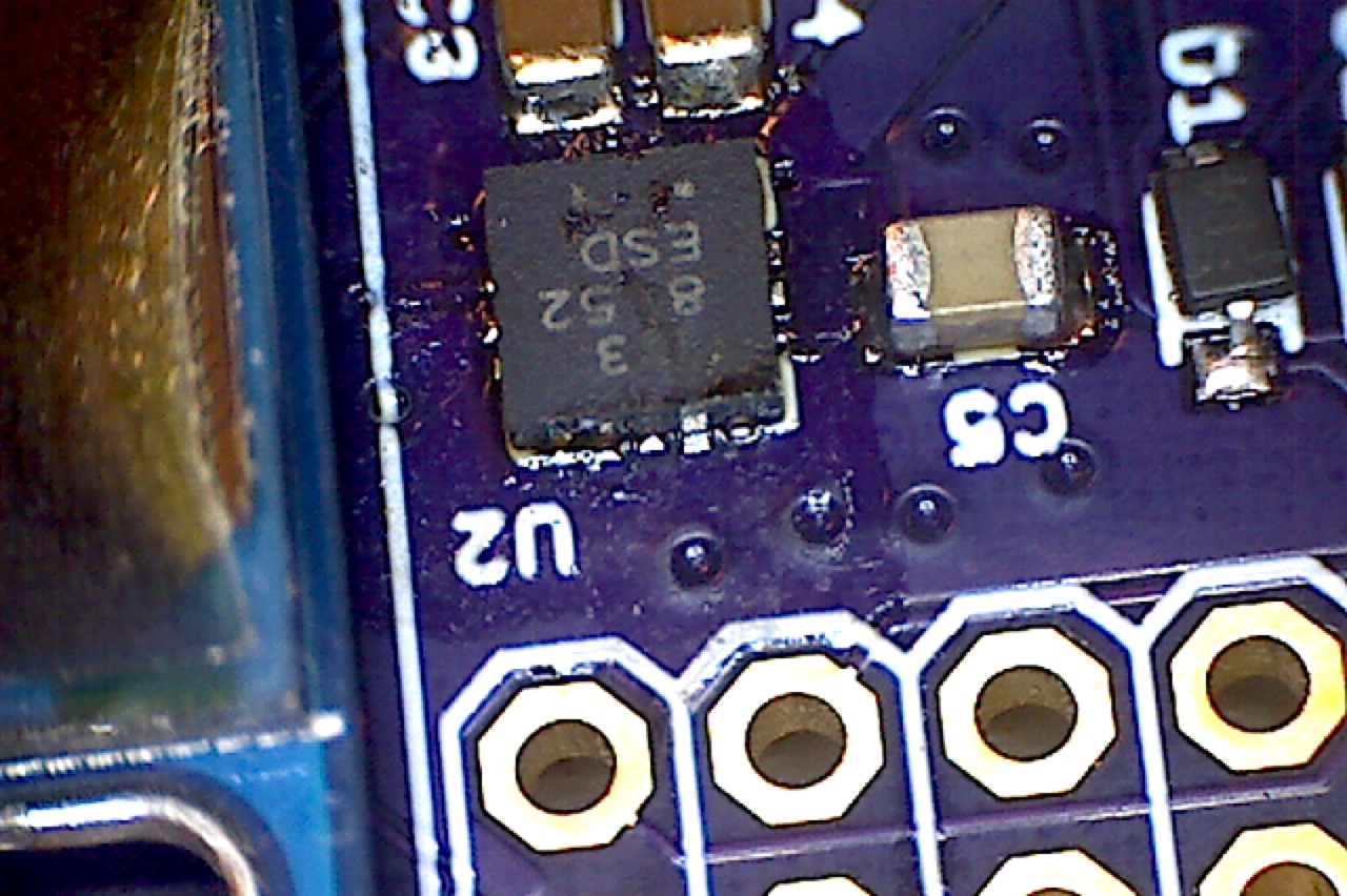
Extend the QFN footprints enough to be able to rework them
If you extend the edge of a QFN pad by 0.3mm past the edge of the chip, you will have some chance to be able to see that the original reflow worked (or didn’t). In addition you will give yourself a small chance to be able to rework it with a soldering iron. For example in the picture below you can see the pin one in from the left has no solder on it. I was able to successfully rework this pin with a soldering iron.
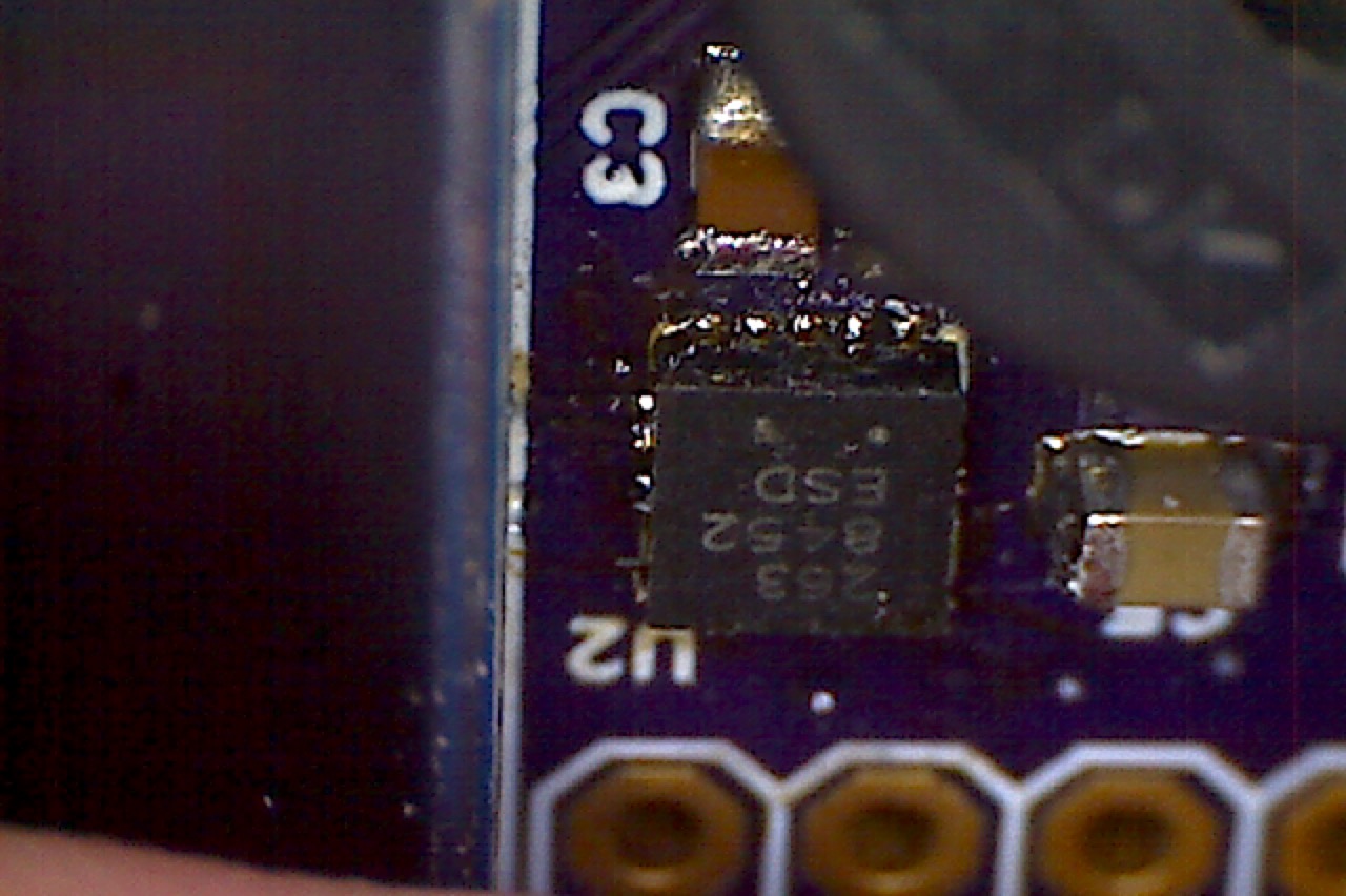
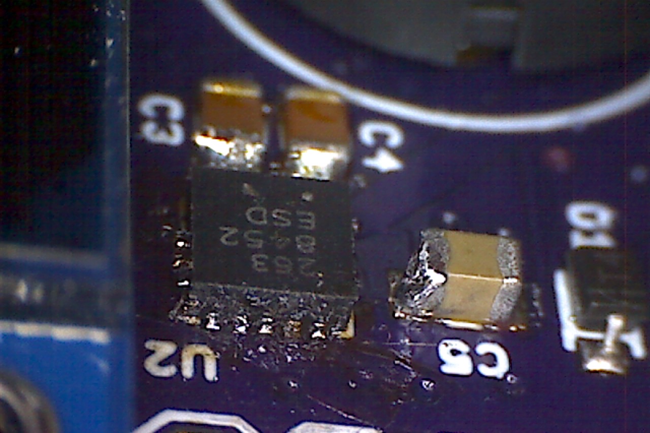
Try not to route under QFNs
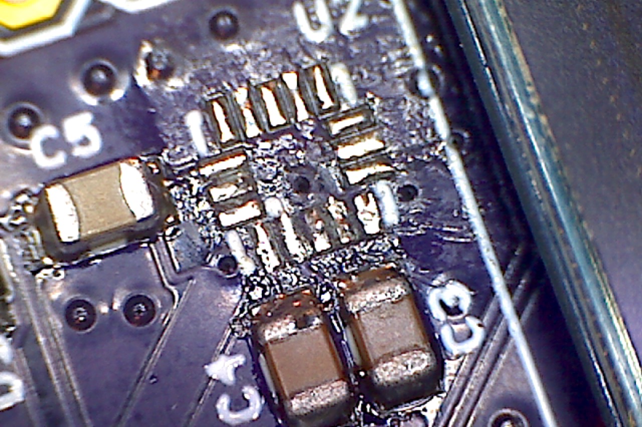
If you have all solder mask under your QFNs it will be much easier to do the original reflow as it will push solder out from under the chip. On tiny pitch QFNs if you have routing you may end up with a messy blob of solder. Here is an example of what not to do.
Try not to use QFN with 0.5mm pitch
Try to use 0.65mm pitch QFNs as they are much easier to reflow. If you use 0.5mm pitch QFNs you are going to struggle to get them correct. If you use a pitch less than 0.5mm then good luck to you.
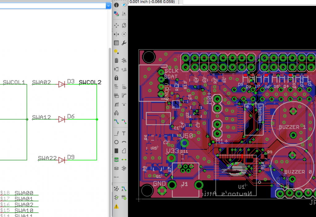
Use the eye tool to compare the schematic and layout
I always open up the schematic and layout in side by side windows. Then I click on each device in the schematic and look at the results in the layout. In the picture below I clicked on “SWCOL2”. This is called cross probing. You should look at each net one by one to make sure that nothing funky happened.
DRC
The Design Rule Checker (DRC) in Eagle PCB works pretty well. USE IT. You can get a rules file from OSH Park (for their two layer process) from their website
You can also use the freedfm.com website to check your files.
Two things that you should be aware of when you run your final DRC.
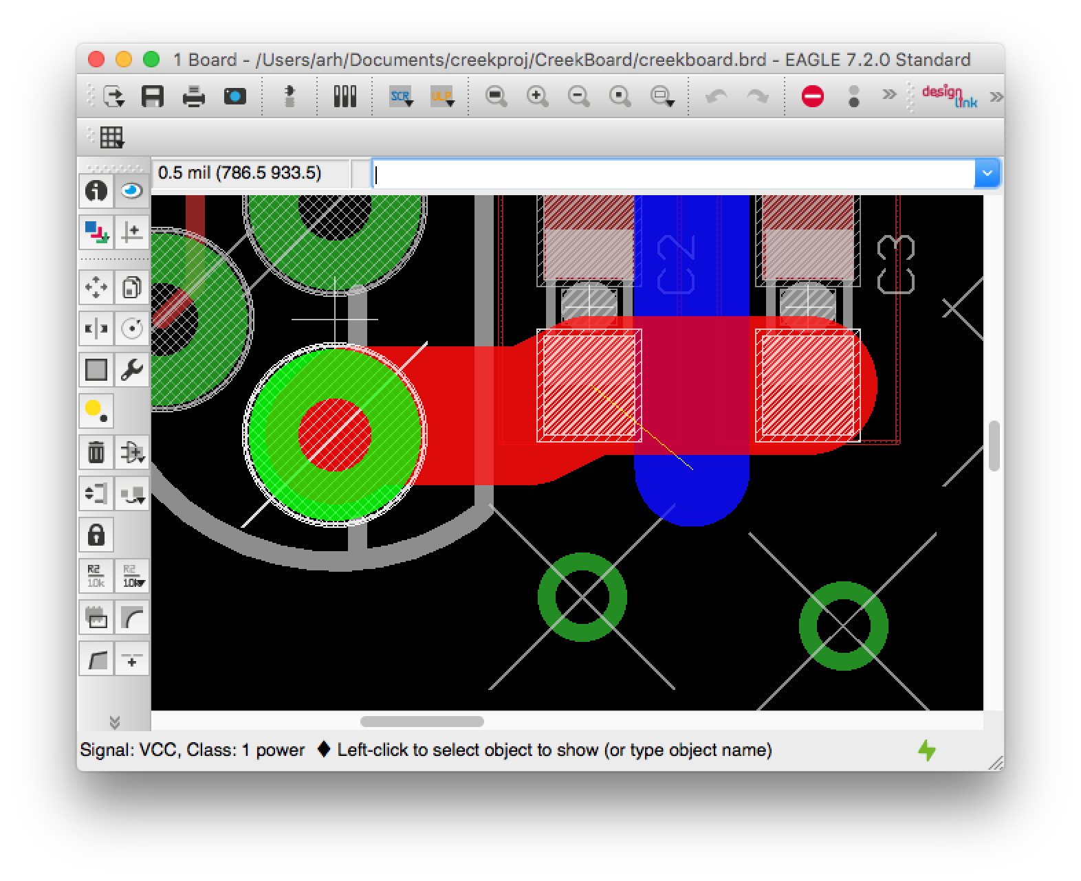
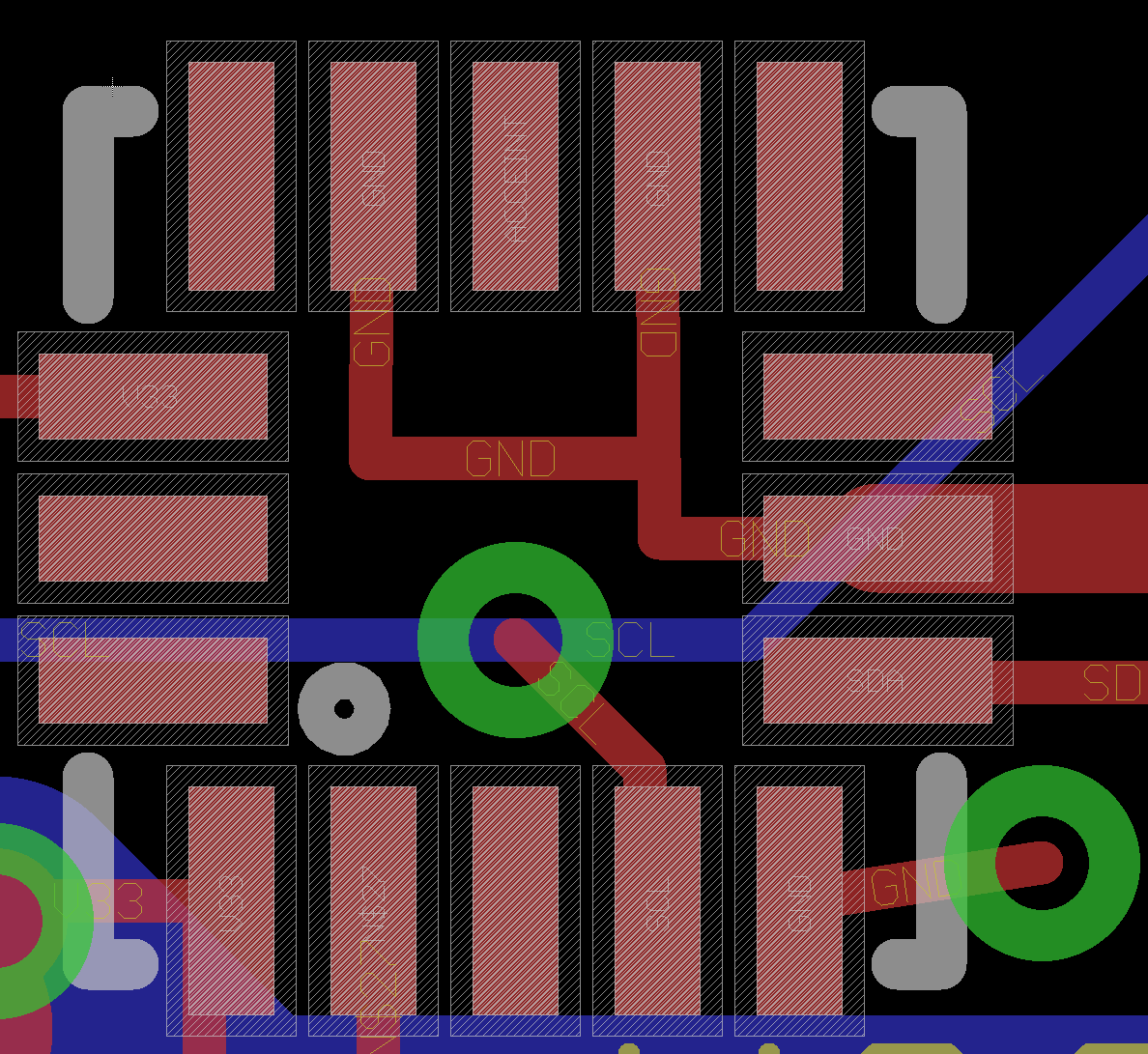
- If you setup a special rule for the power net-clasesses that is greater than the minimum rule you may want to turn it back to the minimum when you run the final DRC. For example, when I setup the ground layer as a power layer, I set the minimum rule to be 40. Before I run the final DRC I set it back to 6.
- For any polygon that is setup as a pour, you will need to set the minimum width of that polygon to be the same as the minimum for the layer. For example: the minimum top metal width at OSH park is 6mil. This means you need to set the minimum width of the ground pour to be 6mil. Here is a screenshot of the corner of the board:
ERC
The Eagle Electrical Rule Checker (ERC) typically catches some problems. By far my biggest problem with the schematics in Eagle is that I occasionally make two wires “connect” by touching, but Eagle doesn’t think that they are connected. The ERC seems to catch this problem pretty well. You should at least run it and go through the errors to make sure that they are false.
CAM Job
In order for OSH Park to make your PCB you need to make Gerber files. Actually, OSH Park can do that for you, but I recommend you do it for yourself so that you are sure what is going to get made. Gerber files are the lingua franca of the PCB business. One file contains one layer for manufacturing, so you will need one file for each layer.
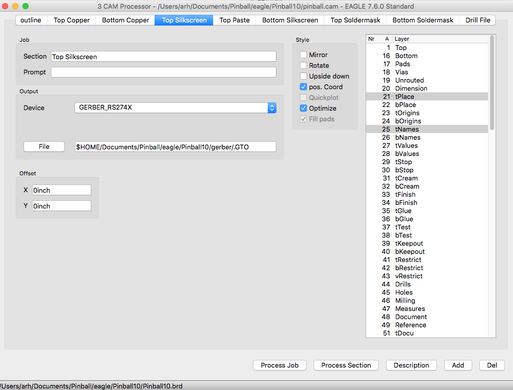
To do maker the Gerbers you need to run the “CAM Processor” which can be found on the tools menu. I reccomend that you start with a preexisting CAM job (like the one that you can download from OSH Park)
The CAM job will have one “tab” for each layer that it creates. In the picture below you can see that I am making the Top Silkscreen. That layer is created by combining “tPlace” and “tNames” onto one layer and then writing it to the file “…/…/…/gerber/.GTO” in the GERBER_RS274X format.
The file naming convention is:
| File Extension |
Description |
|---|
| .GTO |
Top silkscreen |
| .GTL |
Top copper |
| .GBL |
Bottom copper |
| .GTP |
Top Paste (aka the solder paste layer.. you make the solder stencil from this layer) |
| .GBO |
Bottom silkscreen |
| .GTS |
Top Solder Mask |
| .GBS |
Bottom Solder Mask |
| .TXT |
Drill file – used for CNC mill that drills the holes in your board.. this is not a Gerber file |
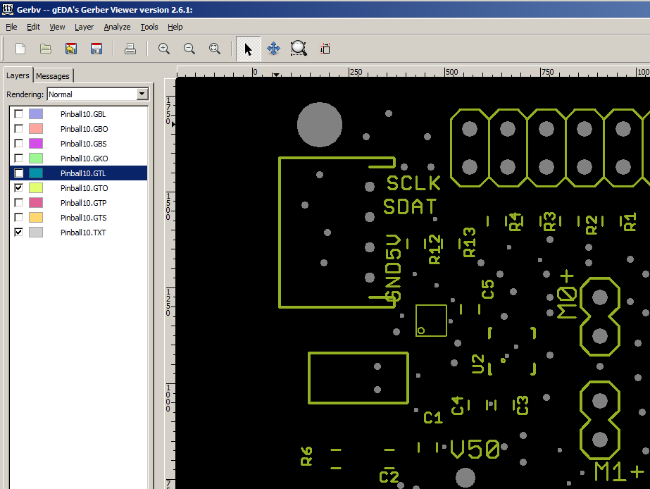
After you have the Gerber files you can look at them in gerbv which is an open source tool.
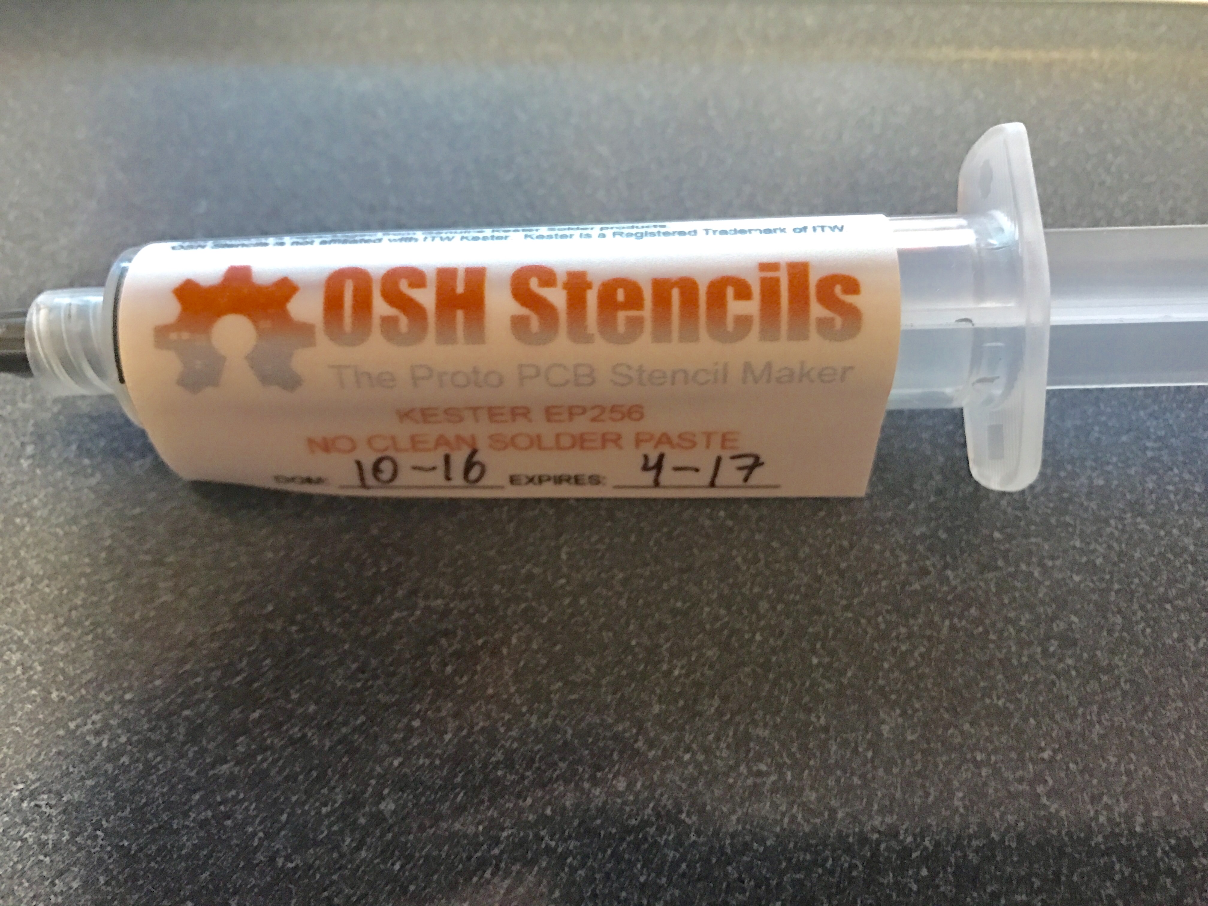
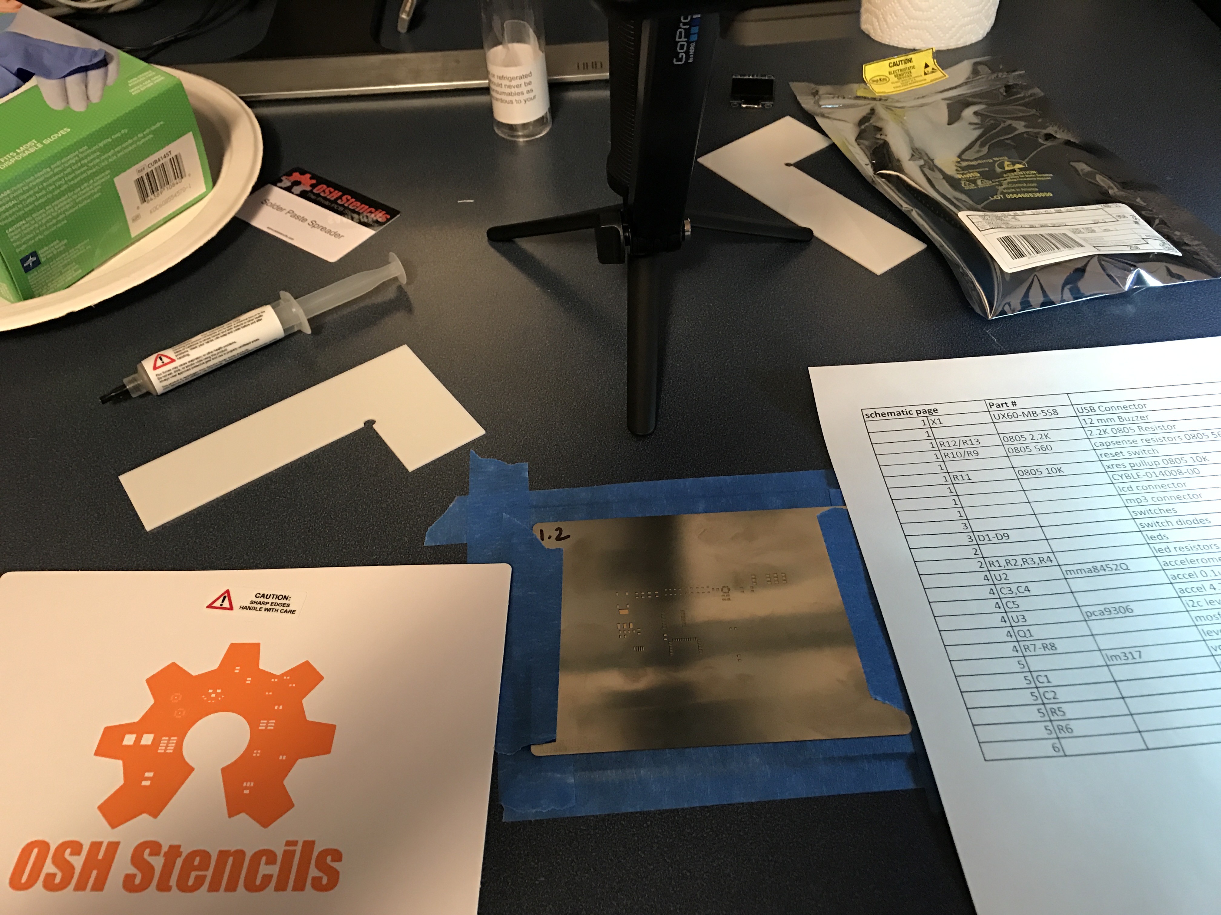
Stencils
Lastly, don’t forget your stencil. I buy mine from www.oshstencils.com which is linked to www.oshpark.com, so you can just select your solder mask from the project that you already uploaded.