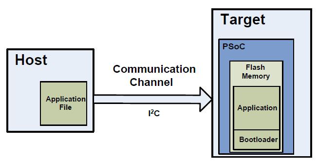
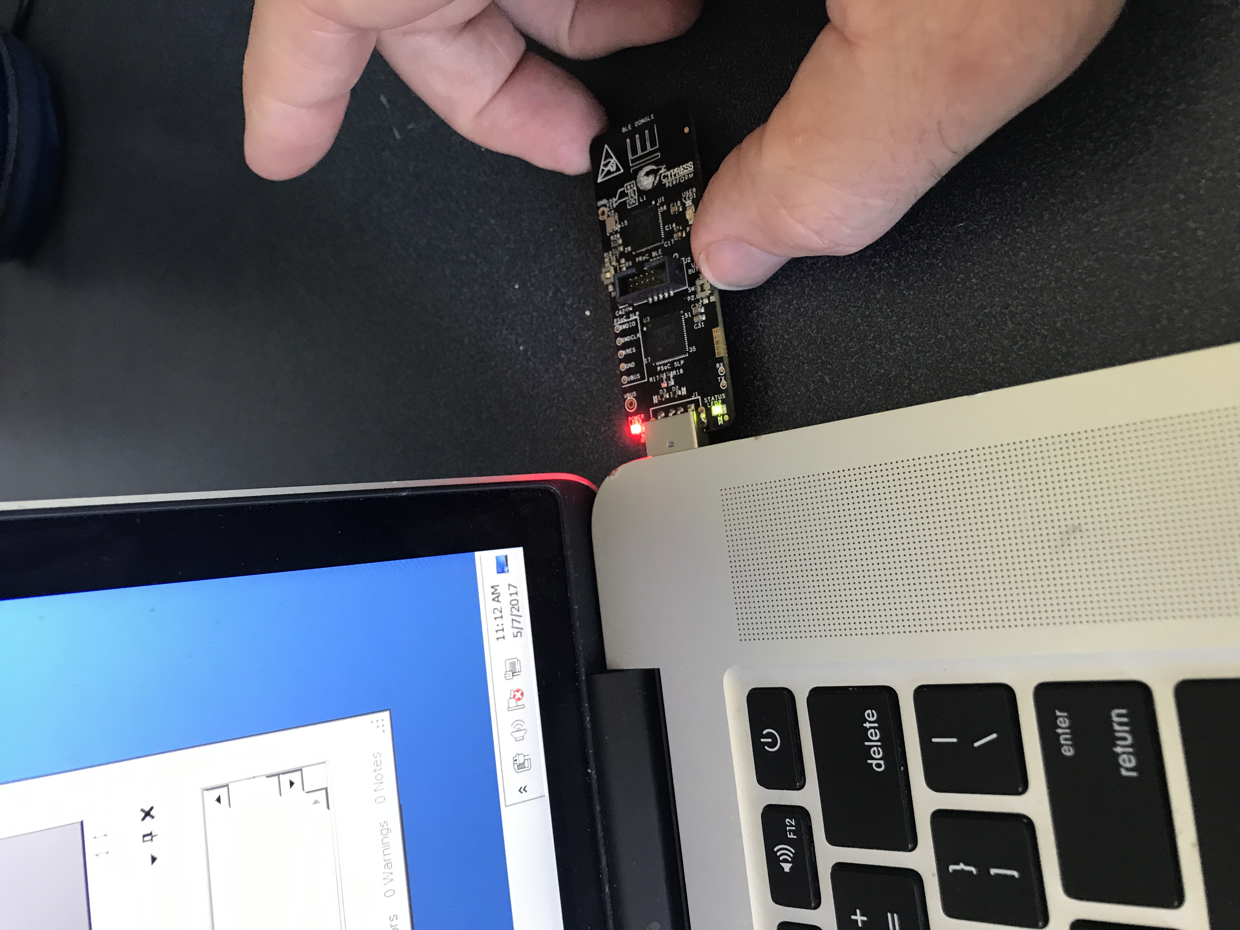
I use PSOC4 to invent all kinds of unique solutions for customers. Usually, they want them field upgradeable to deploy new features or fix bugs. Fortunately Cypress has a great I2C boot loader to meet this need, so I use the heck out of it.
Cypress has a great debugger built into PSOC Creator which fully supports all the ARM Serial Wire Debug protocols such as breakpoints, single step, memory, register viewing etc. However, when you are running a boot loader the debugger does not work! Why not? Because with a boot loader there are two applications resident in PSOC4: The boot loader and application. This is not supported by Cypress implementation of SWD.
Where does this leave you, the intrepid code developer, when debugging a boot loader project? Personally, I have used all kinds of methods: debug UART interface, debug I2C interface, bang out states on pins, debug Bluetooth interface … and on and on. You get the idea. All these methods burn a communications interface and require extra pins on the chip. Sometimes that’s not possible.
The issue recently came to a head when a customer very nearly in production experienced a boot loader failure. One system out of a few thousand was “bricked” when they tried to field update in the lab. Their pinout is frozen, they can’t add new hardware so how do we look inside PSOC4 and see what’s going on?
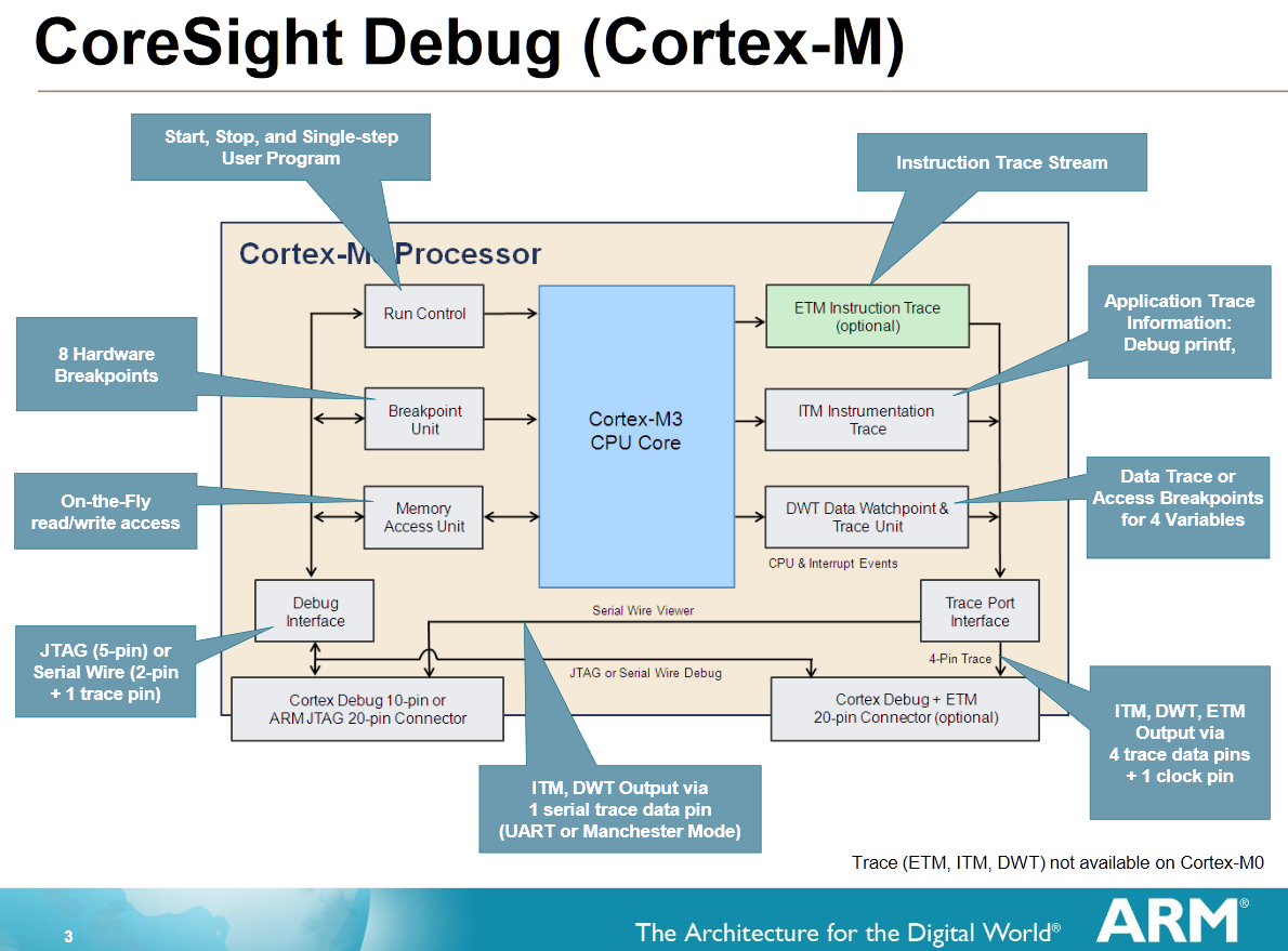
I woke up at 2 AM and thought “Ah Ha! SWV!” (Yes, I Am A Geek) Serial Wire View is an ARM native debug protocol that let’s you XRAY the insides of any ARM MCU with the right interface. SWV is a protocol which runs on the SWD pins (clock and data) but also needs the Serial Wire Output (SWO) pin. Cypress left the SWO pin and associated IP off of PSOC4 to save die cost, foiling my great idea. Brief interlude to drink and bang head on desk.
Fortunately, I don’t give up easily. At least my subconscious does not. Woke up the next night thinking “Ah Ha!” again. Wife was mildly annoyed, but tolerates my idiosyncrasies.
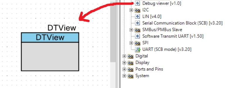
Cypress has a nice software UART transmitter implementation. I shamelessly stole it, modified for my purposes and created a custom component. (It’s pretty easy to do this by the way) Baud rate was modified to 230 KBps and the output pin forced to a specific pin with a control file.
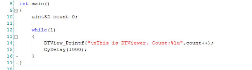
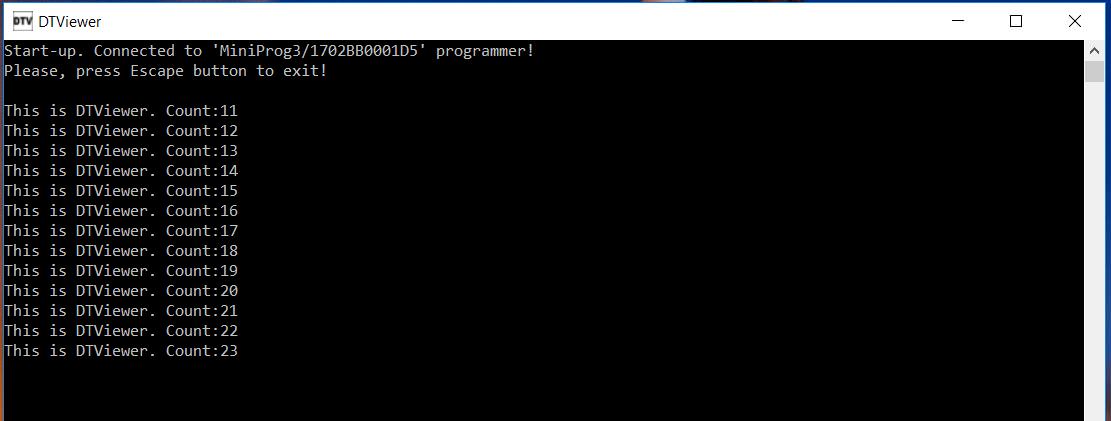
Once the component is in place, you can use its _DView_Printf( ) API call to display any debug data. Here is an example:
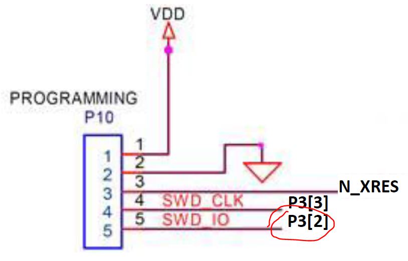
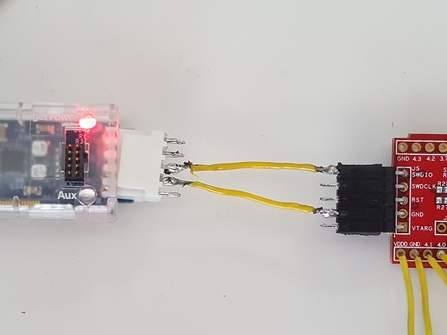
More about that output pin. Cypress sells a tool for programming and debugging PSOC called CY8CKIT-002, aka MiniProg3. The programming connector consists of VDD, GND, reset, SWD clock and SWD data as shown below.
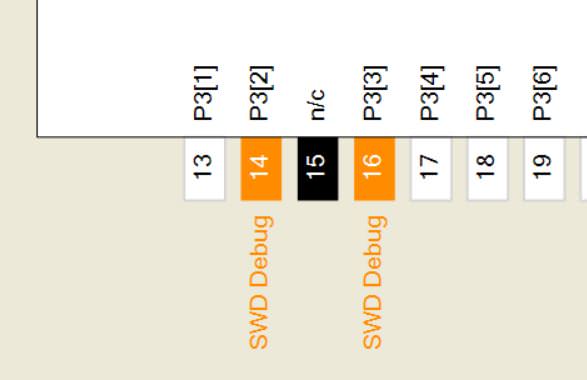
Since we can’t use SWD protocol for debugging anyway, we can change the pins from SWD to normal GPIO. The pins still function for programming. By default they are in SWD mode as shown.
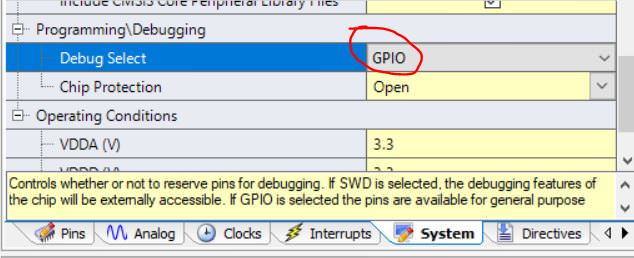
Going to the system tab of the .CYDWR file, we can change them to GPIO.
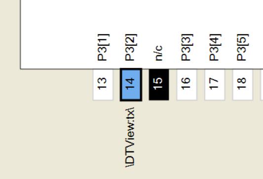
Once we do that, the pins look like this. Here’s the trick. We now assign the TX output of our DTView component to pin 3[2], which is available on the SWD programming header, pin 5.
Can you see where we are going with this? Printf( ) data is now coming out of PSOC4 on pin 3[2], easily accessible on our debug header. This is where MiniProg3 comes in. It can actually receive data as a 230 KBps RX UART on its XRES pin. Weird, right? By building a simple interface cable we can get the data from your debug header into MiniProg3.
MiniProg3 XRES —— SWD HEADER pin 5
MiniProg3 GND —— SWD HEADER pin 2
However, MiniProg3 does not show up as a COM port on your PC, so how do we the data? It needs to be accessed by a host application running the PP_COM API. This is documented under PSOC Programmer Component Object Model COM Interface Guide, Cypress specification 001-45209. If you installed PSOC Creator or Programmer, this document is actually on your PC under C:\Program Files (x86)\Cypress\Programmer\Documents. Engineers don’t like to read instructions. Amazing what you can find when you do.
I wrote a simple console application which opens MiniProg3 using PP_COM, retrieves data from the serial RX pin via USB and displays it like a simple terminal program. Voila! You now have a serial debugger that works for any PSOC4 project using MiniProg3 as your USB to serial dongle.
Customer was really happy with this. We were able to immediately see his problem and fixed it in about 5 minutes.
Finally, here are all the source files
DTView Firmware : PSOC Creator example project and DTView component
Last week I got a question from a customer about how to write into the PSoC 4 Flash. I sent him a fairly straight forward email message explaining the process in English… but after reflecting a little bit, I decided to write an example project as “C’ is often much clearer. And yes I know that this article it doesn’t have much to do with IoT, but hopefully it is helpful to someone. In this article I will explain:
The organization of the PSoC 4 Flash
The risks and issues of writing to the PSoC 4 Flash
A program that demonstrates reading and writing the PSoC 4 Flash
How to protect rows of the PSoC 4 Flash
Organization of the PSoC 4 Flash
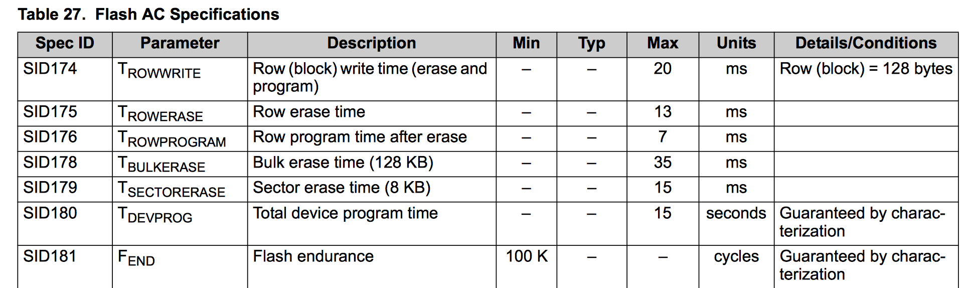
The PSoC 4 Flash is organized into an array that starts at memory address 0x00 and has 128 byte rows. Different versions of the chip will have different numbers of rows and possibly two arrays (in the case of PSoC 4 BLE II). The exact configuration of your part is knowable in the firmware by a set of #defines that are built for you by PSoC Creator. Here is a snapshot from the PSoC 4 System Reference Guide Chapter 8.
You can use that information along with the System call CySysFlashWriteRow() to write into the flash of your device.
Risks and Issues Writing the PSoC 4 Flash
There are several risks that you must take into account when performing a PSoC 4 Flash write (or for that matter writing Flash in any other MCU).
You must write a complete row at a time. In PSoC 4 that is 128 bytes. So, even if you want to write only 1 byte, you will need to read in all of the data surrounding that byte in the row and make sure you don’t overwrite something important.
You can easily write someplace bad and brick your part (e.g. if you overwrite your program, or exception vectors, or …). You need to be very careful that you are writing in the correct place
It takes 20ms, which is a long time in the context of MCU speed, to write a row of flash and the MCU comes to a standstill while that is happening (all of the interrupts are off etc.)
The Flash will eventually wear out. If you look at the data sheet for PSoC 4 you will find that the endurance of the Flash is 100K writes. If you are continually updating a place in the memory, you will eventually wear it out
A PSoC 4 Flash Write Demo Project
To demonstrate the process of a PSoC 4 Flash write I created a project that:
Initializes a 128 byte array in the Flash (aligned to a complete row) with 0’s
Lets you read the Flash array into a RAM array by pressing a key on the keyboard
Lets you printout the values of the Flash array
Lets you printout the values of the RAM array
Lets you increment the values of the RAM array
Lets you write the RAM array into the Flash
Normally when you declare a variable in C it will be assigned to the RAM somewhere (either on the Stack or in the Data or BSS section of the RAM). In order to have my array be assigned to the Flash, I declare the array to be “const”. The first time I did this I did not include the “={0}” in the declaration, and the compiler decided to put the array in the RAM, but when I initialized one of the elements it assigned it to the Flash. The CY_ALIGN() macro tells the linker to put the start of the “row” array on a 128 byte boundary. In other words completely aligning to a Flash row.
// Allocate 1 row of flash... make it aligned to the row size
// and initializde it with 0's
// the const keeps it in the flash (not in the data segment)
const uint8_t row[CY_FLASH_SIZEOF_ROW] CY_ALIGN(CY_FLASH_SIZEOF_ROW) = {0};
At the start of main, I declare array called “data” which will reside in the RAM. I will use this array as a buffer to read Flash data into, then change it, then write it back to the Flash.
We know that the Flash is arranged in rows of 128 bytes (well, actually rows of size CY_FLASH_SIZEOF_ROW). To calculate the row number of the my array “row”, I use the Address of the row divided by the row size. (the CY_FLASH_BASE is 0x00 because the Flash starts at Address 0x00)
    uint8_t data[CY_FLASH_SIZEOF_ROW];
    int rowNum;
    // calculate which row in the flash that the "row" array resides
    rowNum = ((int)row - CY_FLASH_BASE) / CY_FLASH_SIZEOF_ROW;
To make things a bit easier I create a function called “dump” which just prints the values of a “size “of memory in hex format. The function just takes an address that you want to start dumping to the screen.
// This function dumps a block of memory into rows of hex ...16 bytes long in hex
void dump(uint8_t *array, int size)
{
    int i,j;
    j=0;
    for(i=0;i<size;i++)
    {
        dbgprintf("%2X ",array[i]);
        j=j+1;
        if(j==16) // 16 values per line
        {
            j = 0;
            dbgprintf("\n");
        }
    }
    UART_UartPutString("\n");
}
In order to test this whole thing I use a UART to read from the keyboard and display to the screen. The main function is just a loop that reads keys and then does a big “switch”.
When you press ‘f’ it dumps the Flash “row”
When you press ‘r’ it copies the Flash “row” into the array “data” (which resides in the RAM)
When you press ‘i’ it increments the values in the “data” array
When you press “R” it dumps out the values in the “data” array
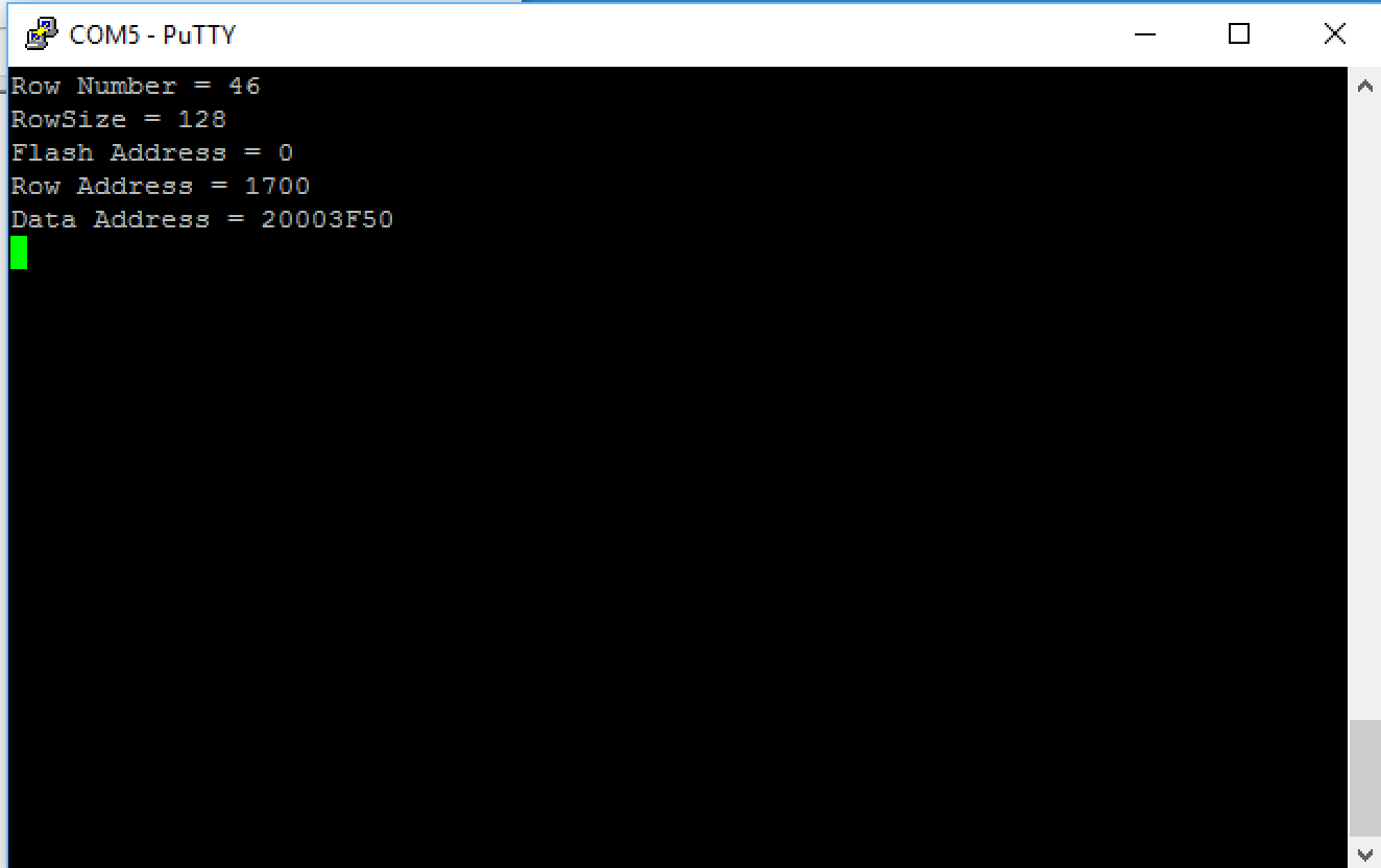
When you press ‘q’ it prints out information about the rowNumber, row size etc.
   for(;;)
    {
        char c;
        c = UART_UartGetChar();
        switch(c)
        {
            case 'f':
                UART_UartPutString("Dumping Flash\n");
                dump((uint8_t *)row,CY_FLASH_SIZEOF_ROW);
                break;
            case 'r':
                UART_UartPutString("Reading Flash into RAM\n");
                memcpy(data,row,(int)CY_FLASH_SIZEOF_ROW);
            break;

            case 'i':
                UART_UartPutString("Incrementing RAM Array\n");
                data[0] = data[0] + 1;
                for(i=1;i<(int)CY_FLASH_SIZEOF_ROW;i++)
                {
                    data[i] = data[i-1]+1;
                }
            break;
            case 'R':
                dbgprintf("Dumping RAM Array\n");
                dump(data,CY_FLASH_SIZEOF_ROW);
            break;

            case 'q':
                dbgprintf("Row Number = %d\n",rowNum);
                dbgprintf("RowSize = %d\n",CY_FLASH_SIZEOF_ROW);
                dbgprintf("Flash Address = %X\n",CY_FLASH_BASE);
                dbgprintf("Row Address = %X\n",(unsigned int)row);
                dbgprintf("Data Address = %X\n",(unsigned int)data);

            break;
When you press ‘w’, it writes the “data” array into the “row” array in the Flash using the “CySysFlashWriteRow()” system call
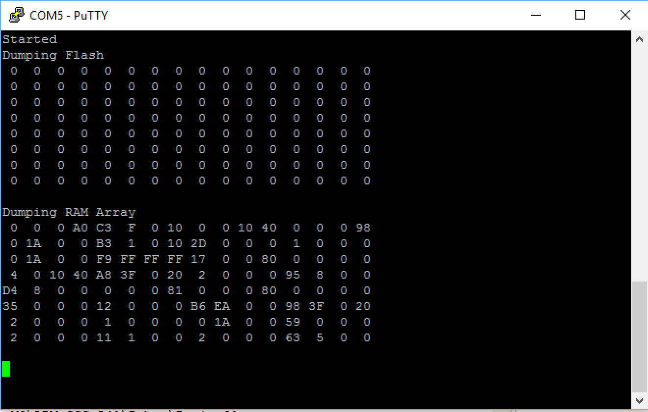
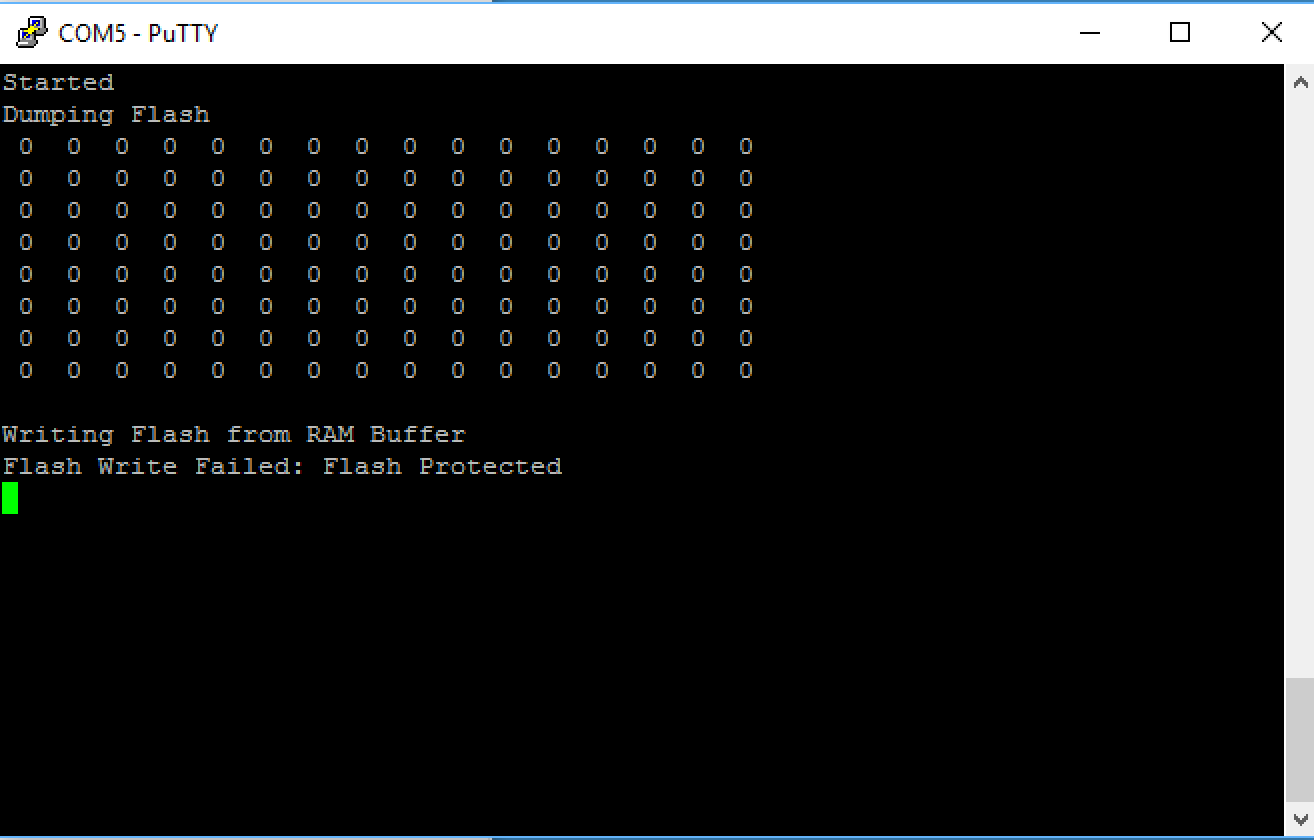
After I program the device, I first press “q” to find out the information about the PSoC 4 Flash array. You can see that my “row” is the 46th row in the Flash and resides at address 0x1700 (as I type this I wish that I hadn’t mixed decimal and hex … and that I had called my “row” variable something other than “row”). You can also see that the rows are 128 bytes and that the Flash array starts at address 0x0. All that is good.
When I press ‘f’ to dump out the Flash array, you can see that my row has all 0’s in it. Then I press ‘R’ to dump out my RAM array and you can see that it has garbly-gook in it (which makes sense as I didn’t initialize the array)
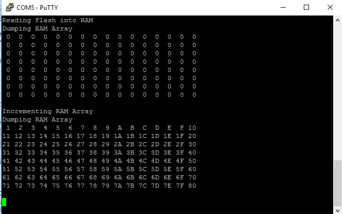
Next, I press ‘r’ to copy the PSoC 4 Flash array into the RAM buffer. Then I press “i” to increment the values in the RAM array, then I dump it out. Lastly, I press ‘w’ to write it to the PSoC 4 Flash.
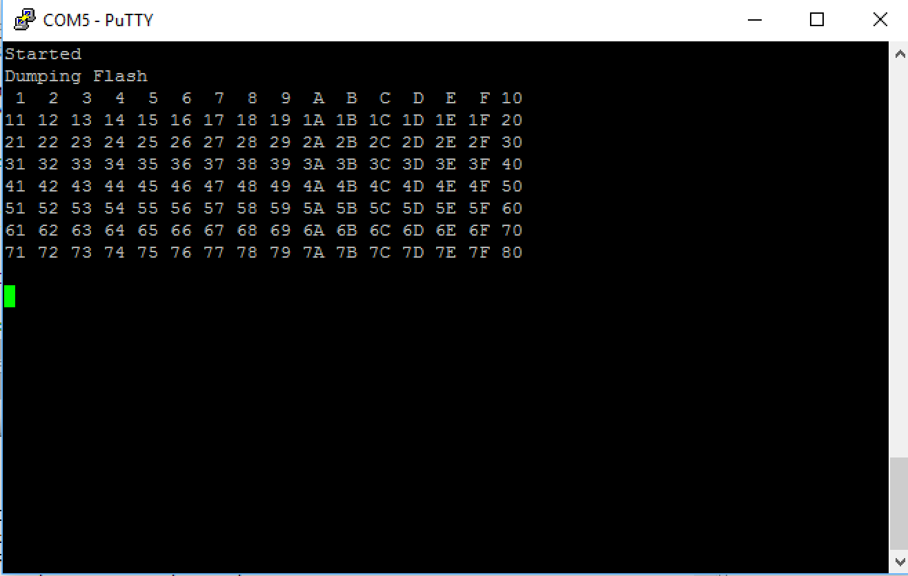
Then I hit reset on the board and press ‘f’ to printout the PSoC 4 Flash array. And I see success, the values were retained in the PSoC 4 Flash even after resetting the device. (or for that matter power cycling it)
Protecting Rows of the PSoC 4 Flash
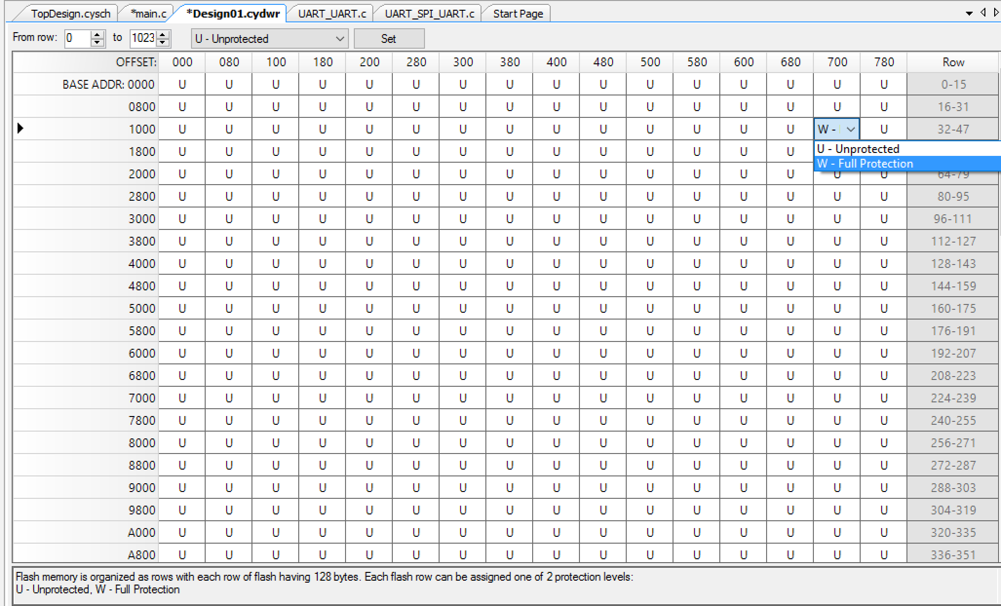
One cool feature of the PSoC 4 Flash is that you can write protect it on a row by row basis. Meaning that you can make it so that the PSoC 4 Flash writing hardware will not overwrite rows. You do this by going to the “Flash Security” tab of the Design Wide Resources. Then you have 1 box for each row in the flash where you can pick “W” for Full Protection and “U” for Writable. In the screen show below you can see me changing the row “ox1700” to Write protection. This is the row where my Flash array resides.
After reprogramming my device I try to press ‘w’ and you can see that the Write fails.
As always my projects are available on the IoT Expert GitHub site git@github.com:iotexpert/PSoC4-Flash-Write-Example.git
In the previous article I showed you how to build PSoC4 BLE Central firmware to talk to a BLE Peripheral. When I did that firmware I built it to program into a CY8CKIT-042-BLE kit. What I should have done was made the firmware work with the CySmart Dongle. An error that I will fix in this article.
In this article I give you an introduction to the CySmart dongle, then I will show you how to:
Update the firmware on the dongle (both KitProg and the PRoC)
Use the PC to debug a PSoC4 BLE Peripheral
Modify the PSoC4 BLE Central Project to work on the CySmart Dongle
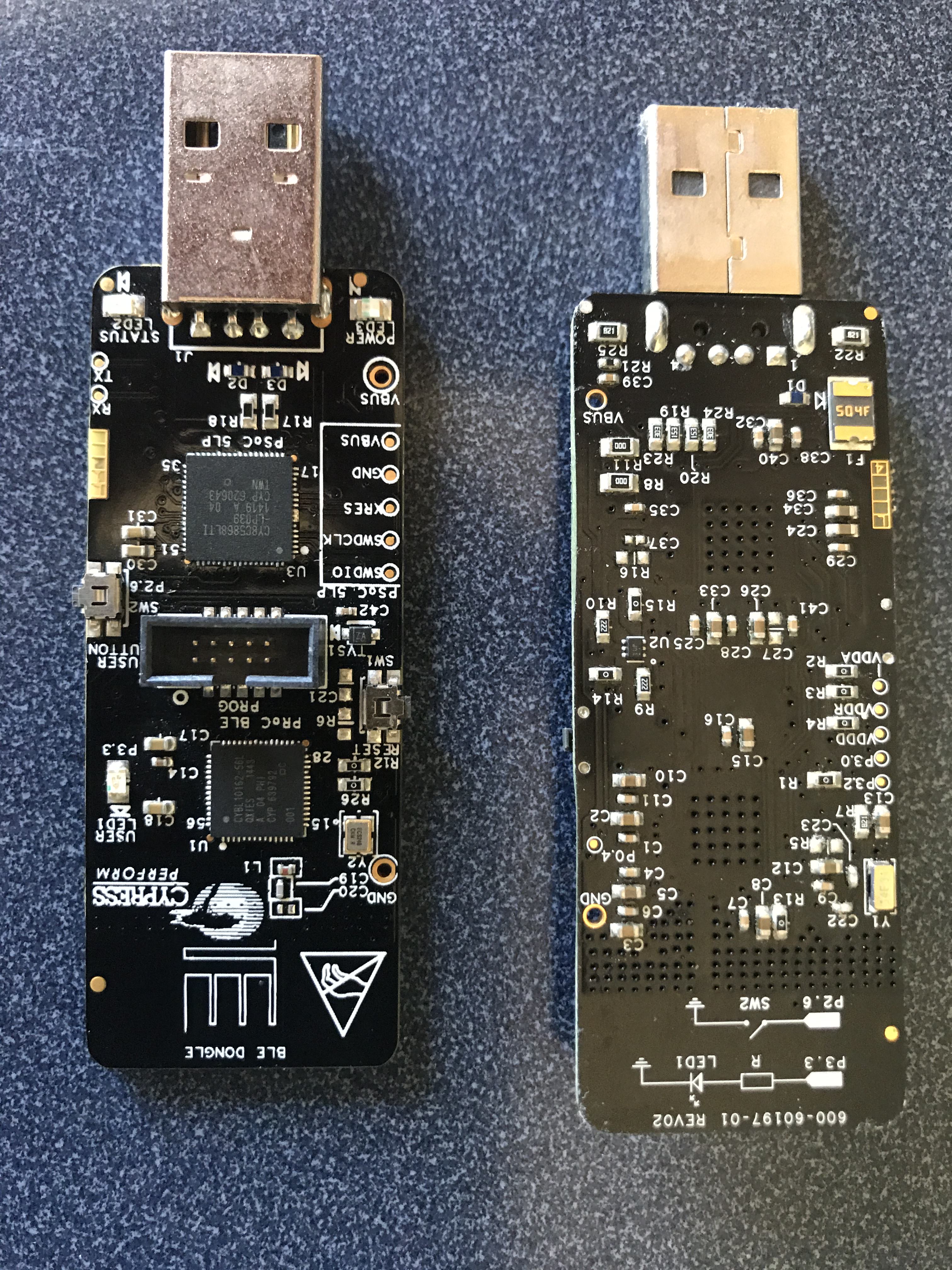
CySmart Dongle
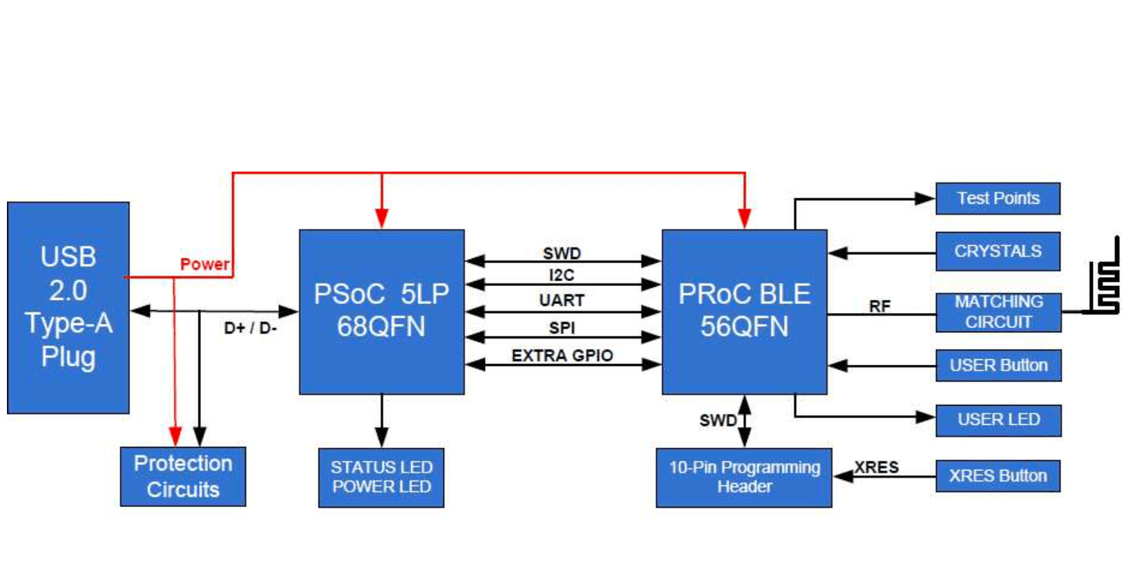
As you can see in the picture above, the CySmart dongle is a USB dongle with a PRoC BLE Radio on it. It uses a PSoC5 programmed with the KitProg firmware to bridge from the PRoC to the PC. In the diagram below you can see that it can bridge SWD, I2C, UART and SPI. In addition the dongle has 1 user button and 1 user LED. This is perfect for the PSoC4 BLE CapSense LED GAP Central Project that I built in the previous article.
You get the CySmart dongle as part of the CY8CKIT-042-BLE Kit. The dongle comes programmed with the CySmart Firmware which enables you to connect to the CySmart PC Program (more later in this article).
There are two version of the dongle
CY5670 with PRoC & 128K of Flash
CY5671 with PRoC & 256K of Flash
Update the CySmart Dongle
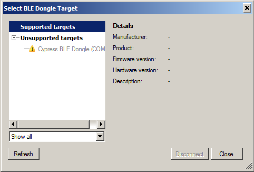
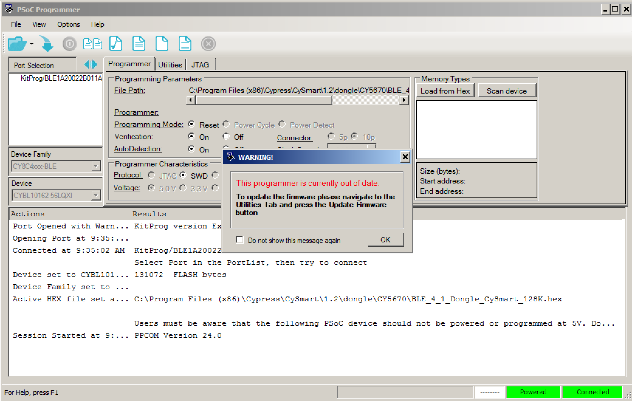
Literally (well almost) every time I plug in a CySmart dongle, I get this message telling me that it is an “Unsupported Target”. This means that the firmware is out of date and needs to be updated.
In order to fix the firmware, you need to quit the CySmart program, then start the PSoC Programmer software. And, I also find that every time I start PSoC Programmer that the KitProg firmware is out of date. To fix this press OK.
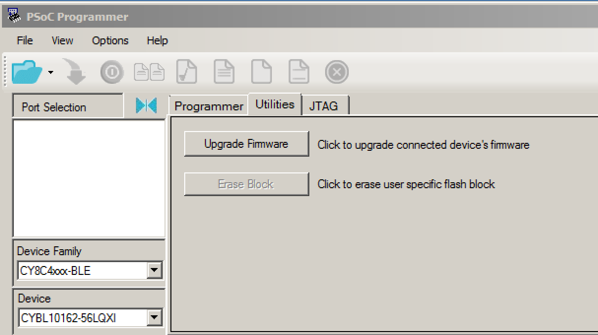
Then click the “Utilities” tab, then “Upgrade Firmware”
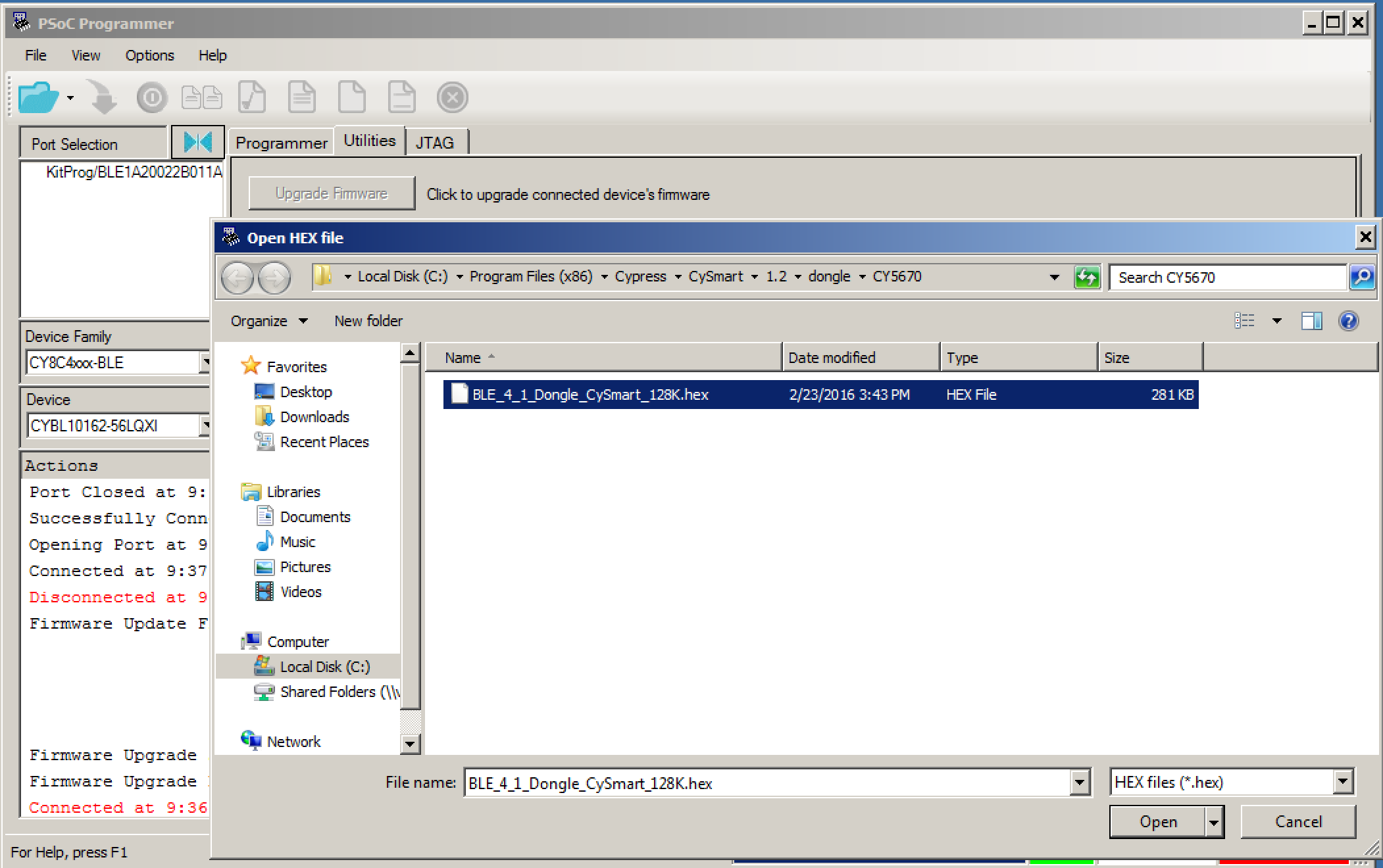
Once the KitProg firmware is up to date, you can then program the CySmart firmware. Press the “folder” button, then navigate to the firmware which lives in Program Files(x86) –> CySmart –> 1.2 –> dongle –> CY5670. Then press the “down arrow” which means “download the firmware”. Once that is done, you are good to go with running CySmart (quit PSoC programmer so that it can talk to the dongle).
Use the PC CySmart to Debug a PSoC4 BLE Peripheral
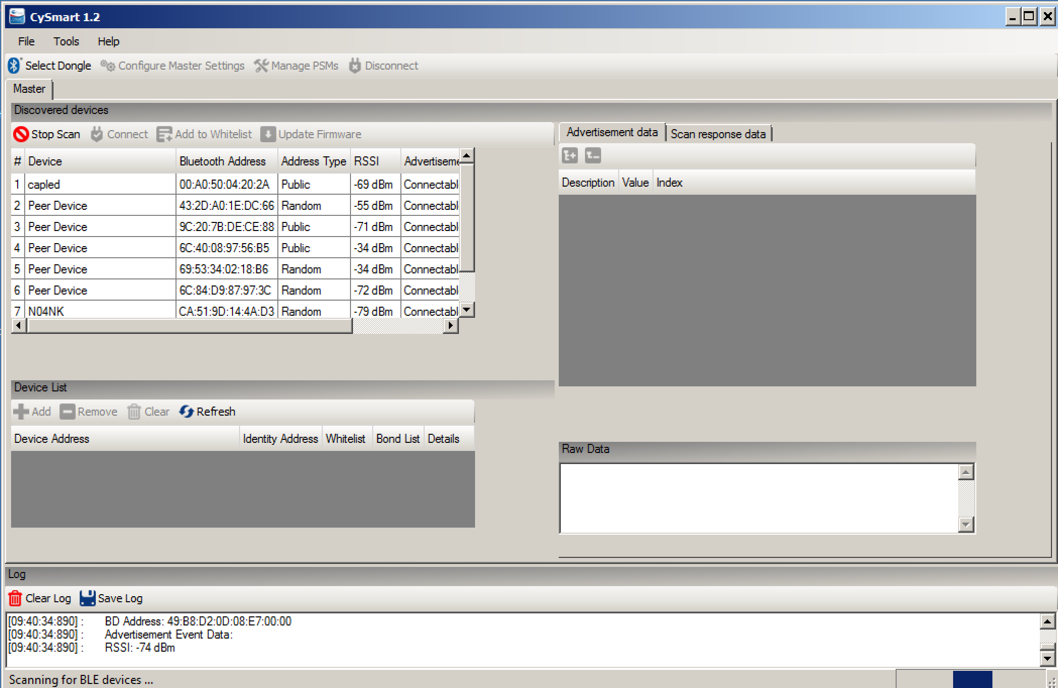
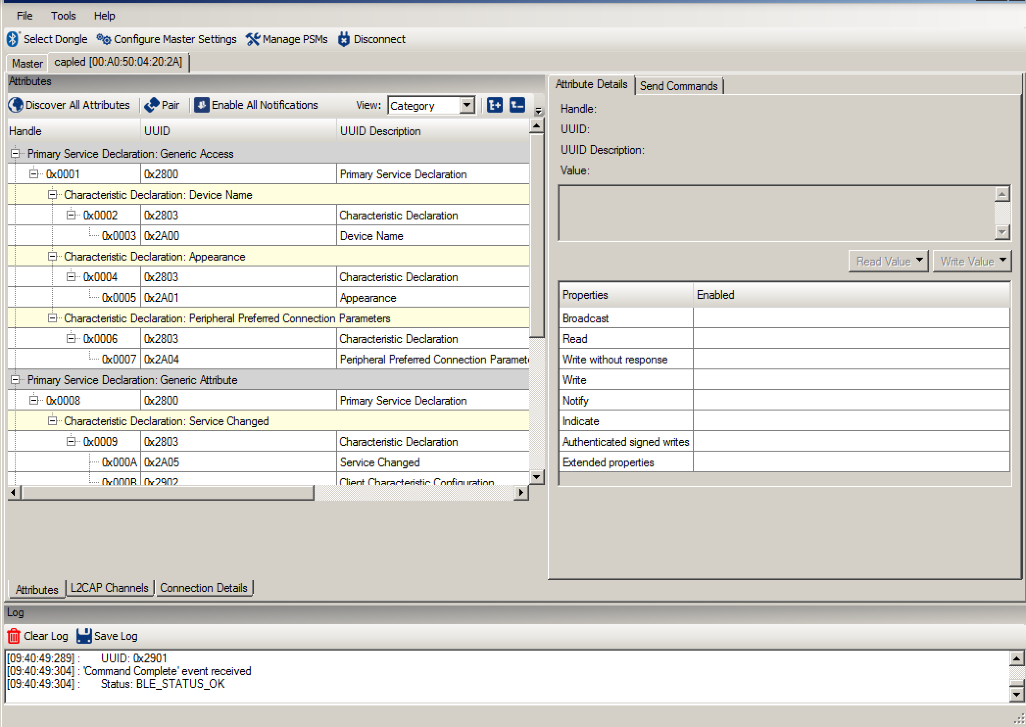
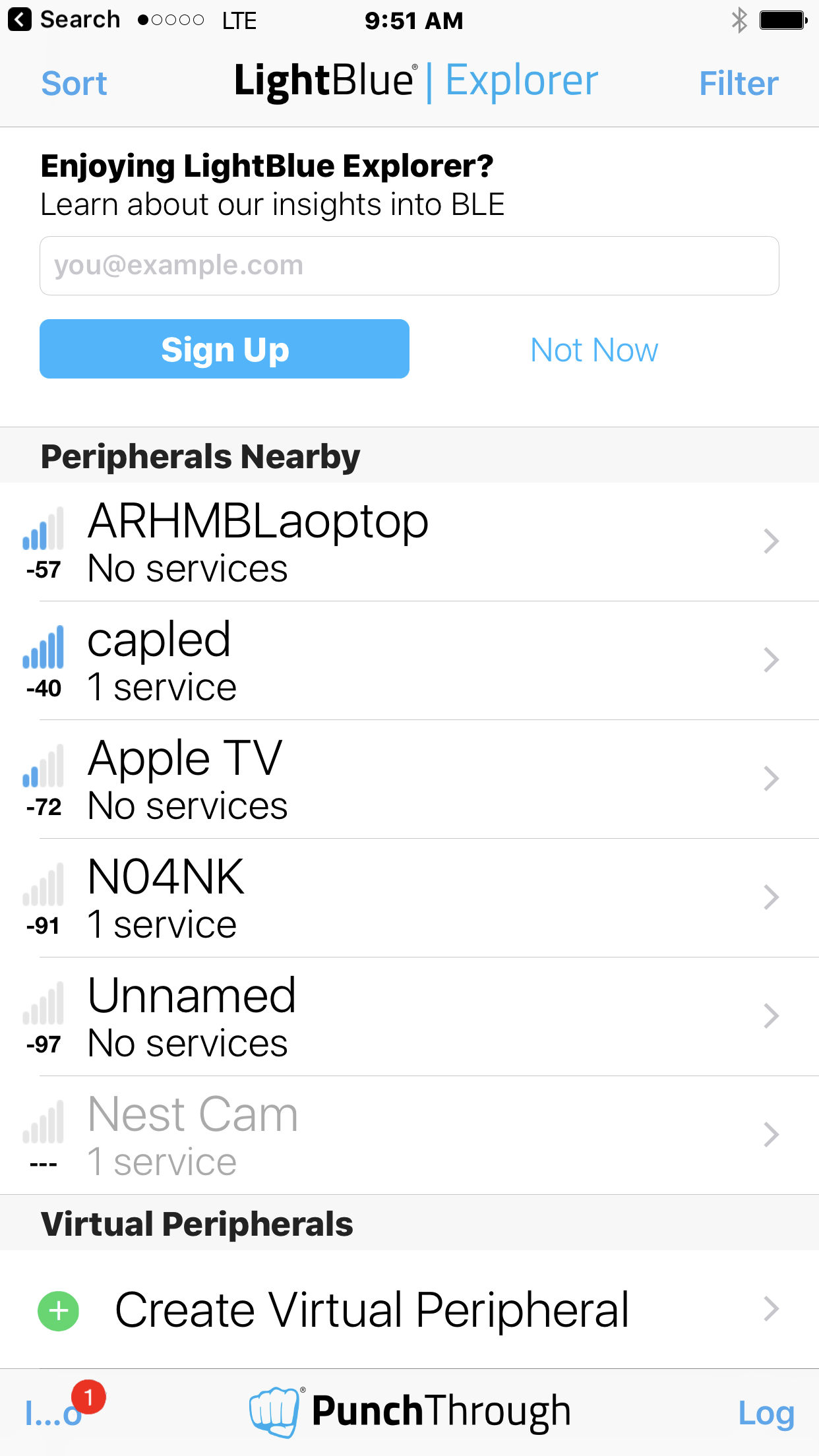
Now that I have a functional CySmart dongle, I can run CySmart. This is a Windows PC Version of a GATT browser (like the CySmart iOS/Android App or the LightBlue app that I used in the previous article). In CySmart press “Start Scan”. In the picture below you can see all of the BLE peripherals that CySmart can see, including the “capled” project.
Once I click on “capled” and then “connect” and finally “discover all attributes” I will get a window that looks like this. You can see all of the GATT Database.
After that I can Read and Write attributes (like the LED Attribute) by typing the value I want to write into the box on the upper right, and pressing “Write Value”. For example you can turn on the LED by writing a “1” into the LED characteristic.
Modify the PSoC4 BLE Central Project to work on the CySmart Dongle
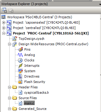
Next, lets modify the original project so that it can work on the dongle. I will start this whole process by doing a copy/paste of the “centralled” project. Then renaming it to “PROC-Central”
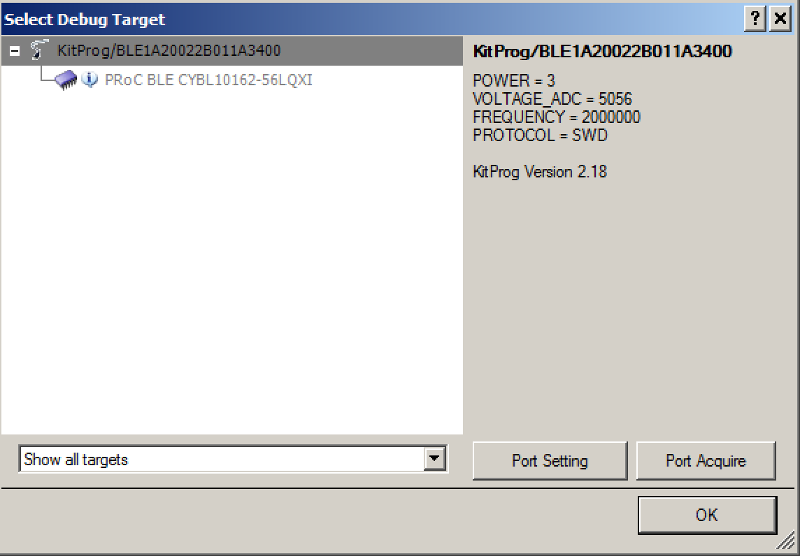
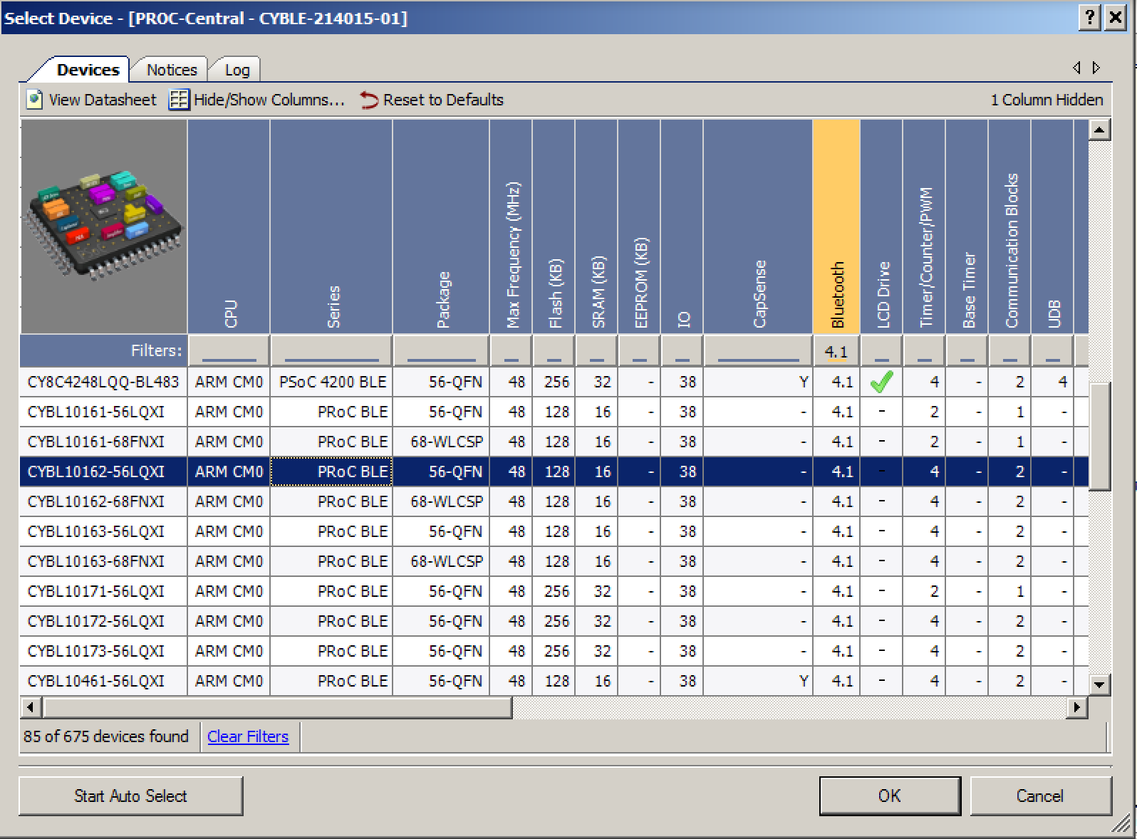
The dongle has a PRoC instead of a PSoC4 BLE. This means you need to run the device selector and change the target device. I can never remember which version of PROC is on the dongle. So, to figure it out I click the program button, which brings up this screen that says my project isn’t compatible with the target. It also tells me that this dongle has “CYBL10162-56LQXI”
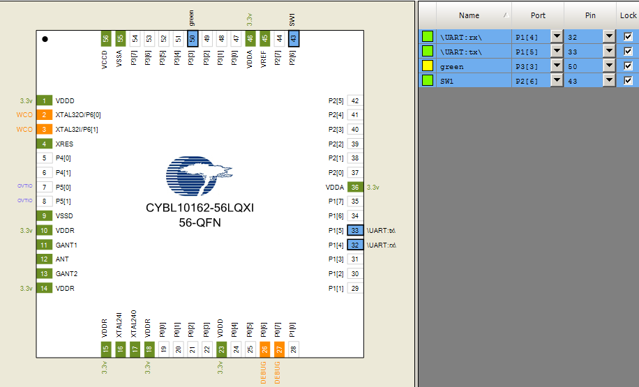
Now go to “Project –> Device Selector” and change to the “CYBLE10162-56LQXI”
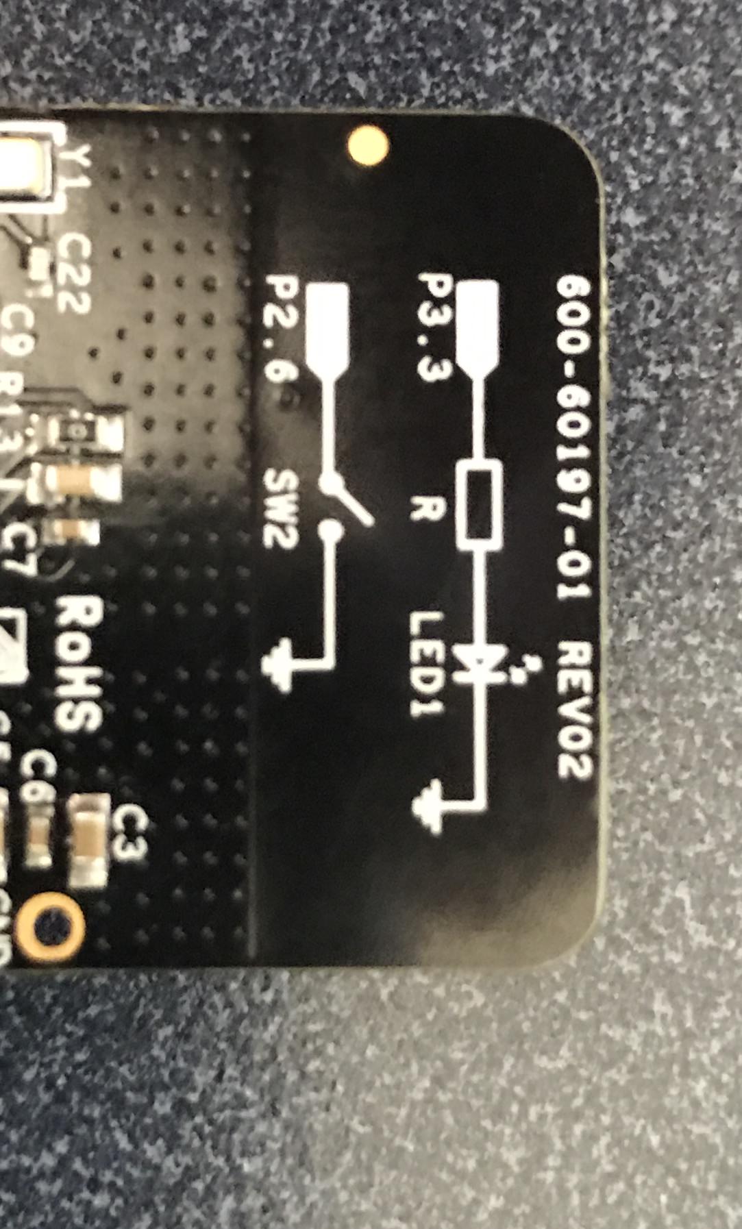
The pin assignments are a little bit different. On the back of the board you can see that we put a handy-dandy picture showing the arrangement for the LED and the button.
But unfortunately we didn’t show you the pins for the UART on the silkscreen. But you can find those in the schematic (which can be downloaded from the website)
Now you can assign the correct pins (noticed that I deleted the red/blue LED pins because they don’t exist on the dongle)
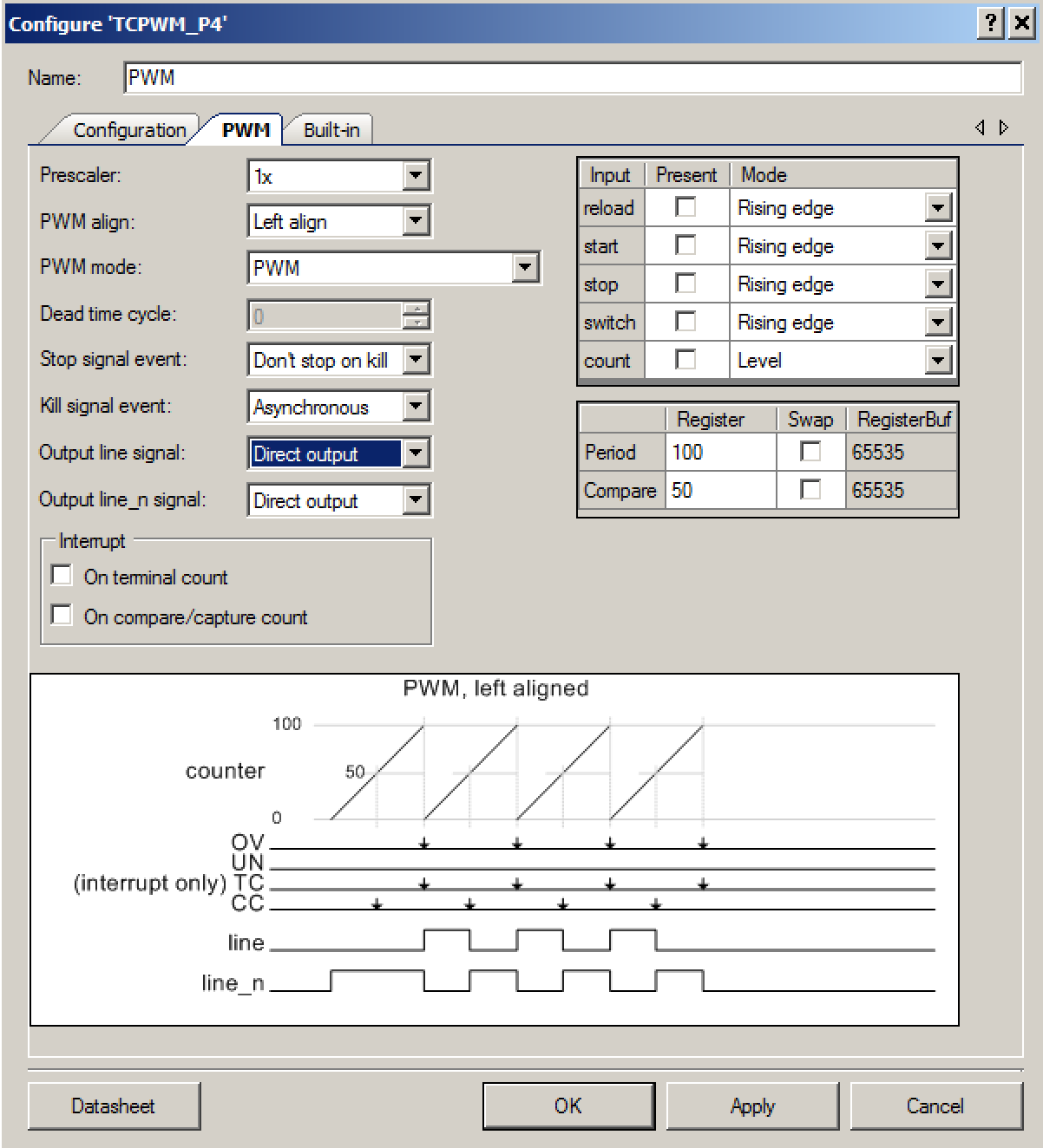
Finally you need to change the PWM to be active high instead of active low.
Now program and test it. The user switch is the tiny little button under my thumb.
As with the previous article you can find all of this source code on the IoT Expert Github site or git@github.com:iotexpert/PSoC4BLE-Central.git. In the next article I will start the process of building a GATT Browser inside of a PSoC4 BLE.
Last week I got a nice email from a Cypress customer in Italy (I think). He asked about implementing a PSoC4 BLE Central. I replied that it was pretty easy. Over the weekend I thought about it a little bit more and realized that I had never implemented the Central a.k.a. the “other” side of a BLE connection in a PSoC. I had always built the Central side in an iPhone application written in Swift or Android application written in Java. So it seemed like a good thing to do to implement it in C. It turned out to not be quite as easy I had hoped because of some problems in the Cypress documentation. In the next several articles I am going to show you how to implement a PSoC4 BLE Central.
I am going to use the project from the video series called “capsenseled” as the GAP Peripheral and then I am going to show you how to write the GAP Central code. You can learn about the GAP Peripherals in the video series called “PSoC® 4 BLE 101 Video Tutorial Series: How To Create Products Using PSoC 4 BLE“. Here is the first video from YouTube.
In that series of videos I showed you how to build a custom GATT profile for Capsense and an LED. The GAP Peripheral has an LED that you can control from the GAP Central, and it has a Capsense slider that you can read its value from the GAP Central. You can “git” all of the source for this project from the IoTExpert Github website or git@github.com:iotexpert/PSoC4BLE-Central.git
In this article I will show you:
The GAP Peripheral and GATT Database
How to build the schematic for the GAP Central
How to configure the BLE component for the GAP Central functionality
The steps required in the firmware to read and write the GAP Peripheral
The GAP Peripheral and GATT Database
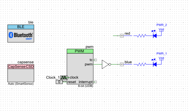
To start the process I will “git” the source code for this GAP Peripheral from the IOT Expert Github site. Then, I open the project called “capsenseled” in PSoC Creator. The schematic has:
The Capsense component which controls the slider
A PWM that drives the blue LED to serve as a notification of the state of the BLE (blinking means advertising)
A red LED which can be turned on/off from the GAP Central Side
The BLE Component
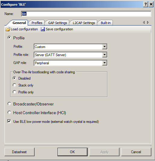
The BLE Component is configured to be:
A GAP Peripheral
with a GATT Server
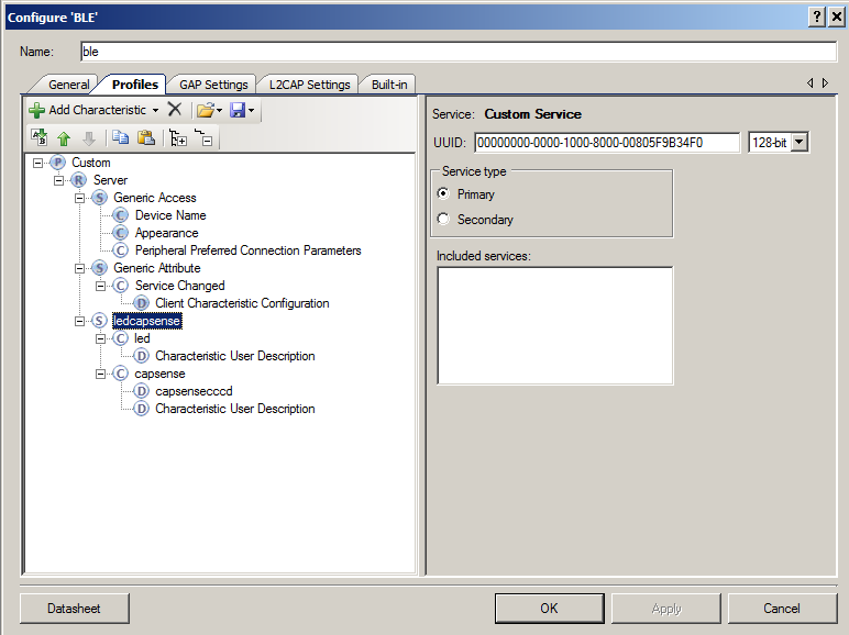
The GATT Database is setup to have:
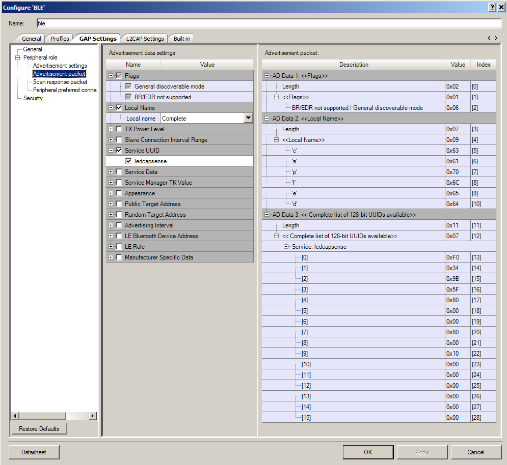
A custom service called “ledcapsense”
A custom characteristic called “led” (a uint8)
A custom characteristic called “capsense” (a uint16)
The advertising packet is setup to advertise
The name of the device “capled”
The fact that it has a GATT Service called “ledcapsense”
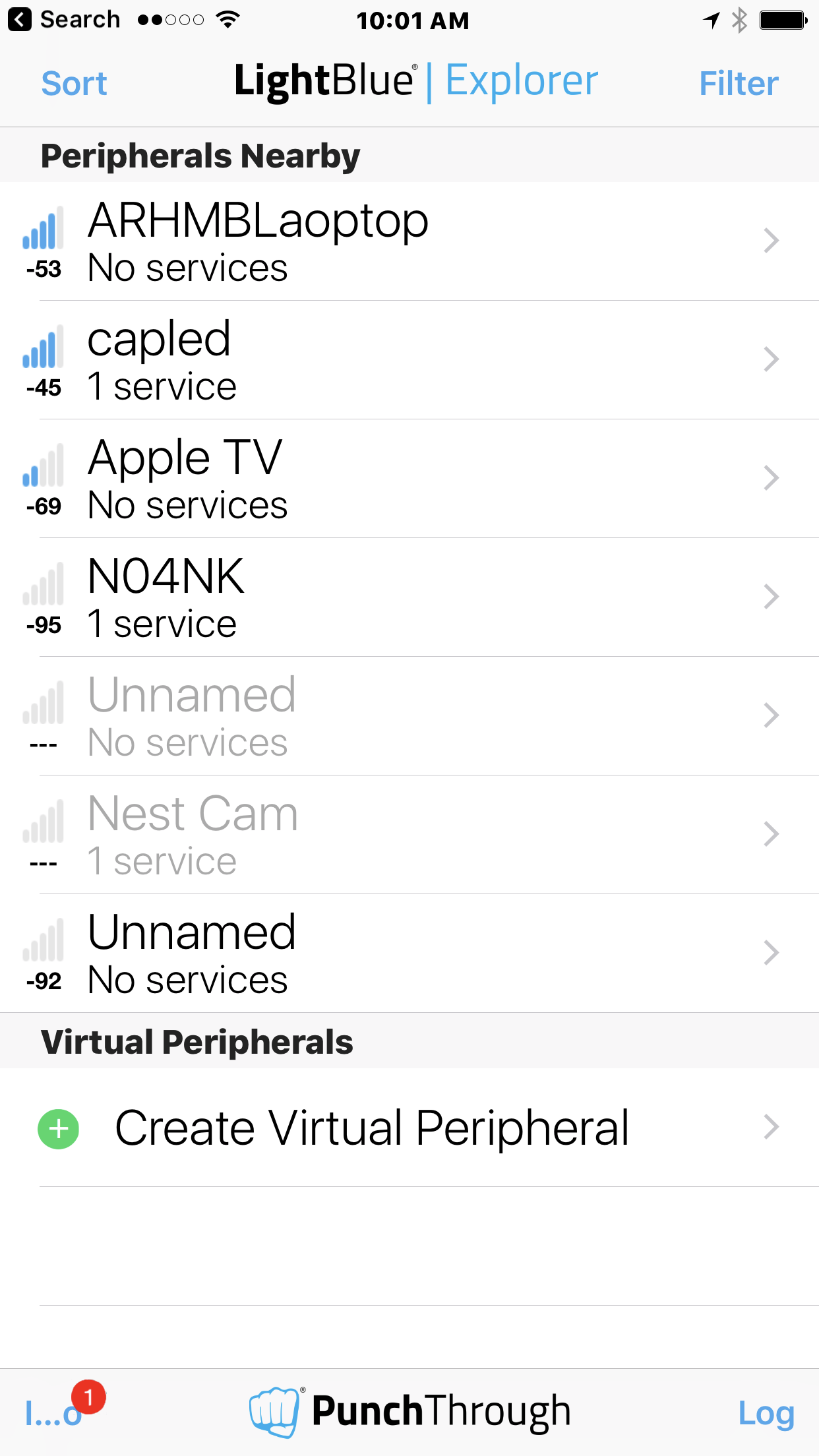
When you program this project you will get a blinking blue LED (that says the BLE is advertising). When I run “lightblue” I can see the “capled” advertising:
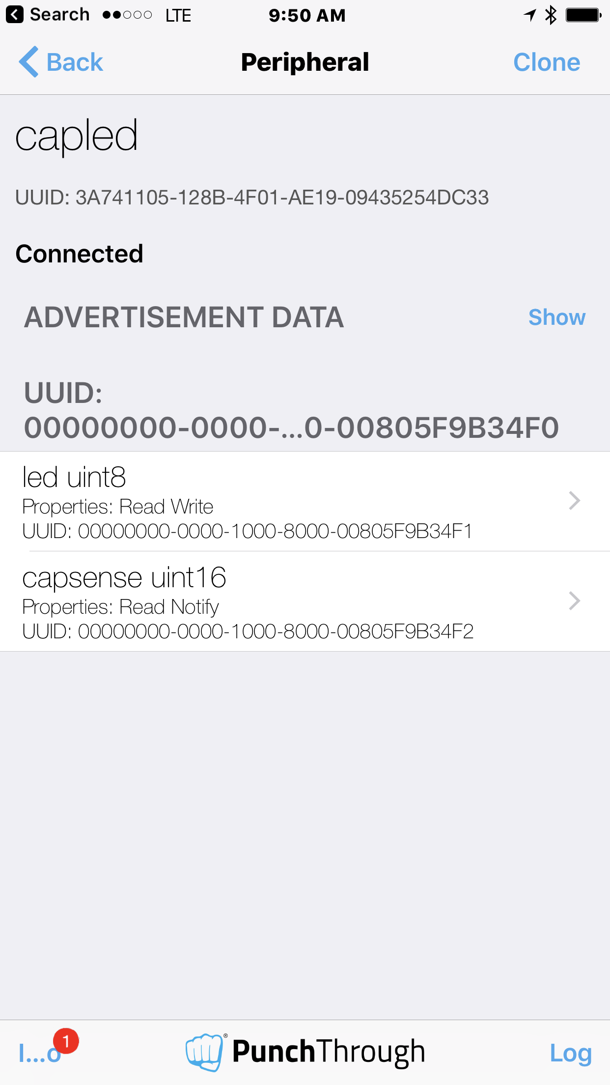
After I connect the device I can see the UUID of the custom service & the two characteristics:
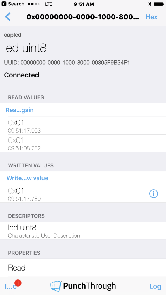
Finally I can read/write the led characteristic.
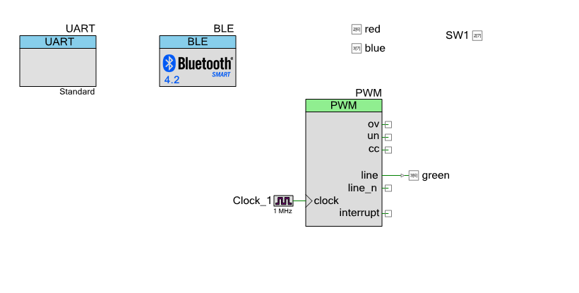
PSoC4 BLE Central Schematic
To make my PSoC4 BLE Central I build a project for the CY8CKIT-042-BLE (you can see all of the source code in the project called “centralled”
Start by building a schematic with
A debug UART (I will print to the terminal program)
The red/blue/green led pins
The mechanical button pin (called SW1)
A PWM to drive the green LED (it will vary the brightness of the LED based on the capsense value on the GAP Peripheral)
The BLE Component
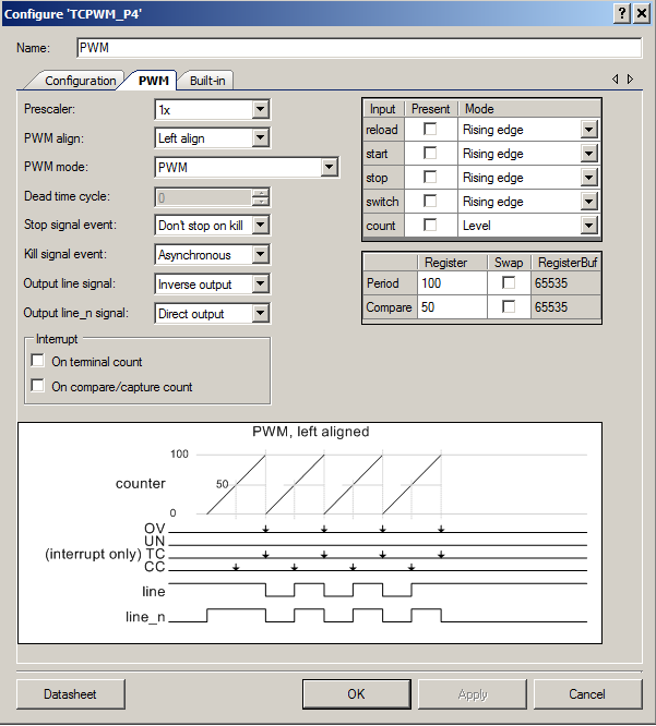
Configure the PWM (to vary between 0 and 100% brightness) with inverted logic (because the LED on the board is active low)
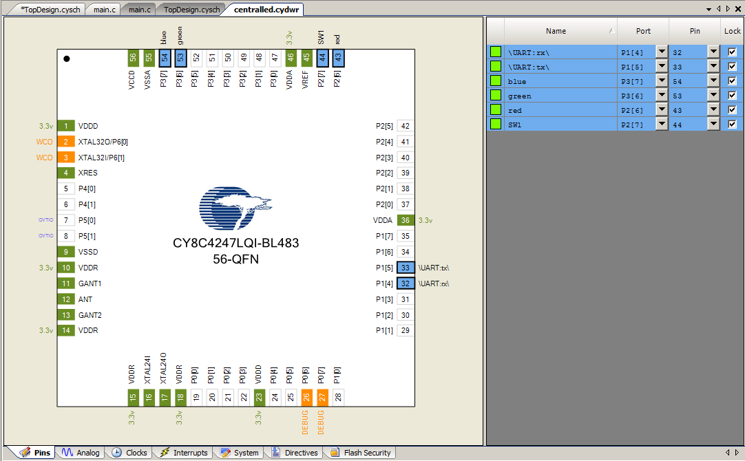
Assign the Pins:
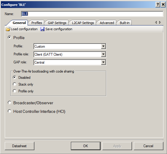
You will need to configure the BLE to be a:
A GATT Client
A GAP Central
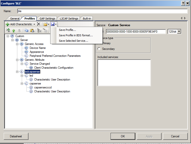
If you tell the BLE Component what the GATT Server configuration looks like (on the GAP Peripheral side) it will make the service discovery firmware much simpler. To do this, go to the GAP Peripheral project and export the “ledcapsense” service from the Peripheral into an xml file (see the Save Selected Service…)
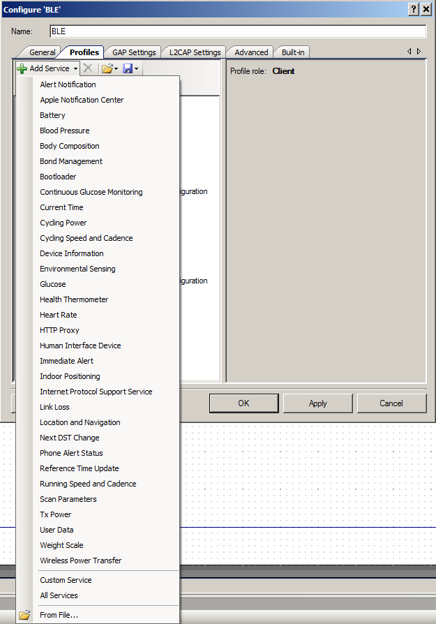
Then go back to your PSoC4 BLE Central project and add a new service “From file” (see at the bottom of the menu)
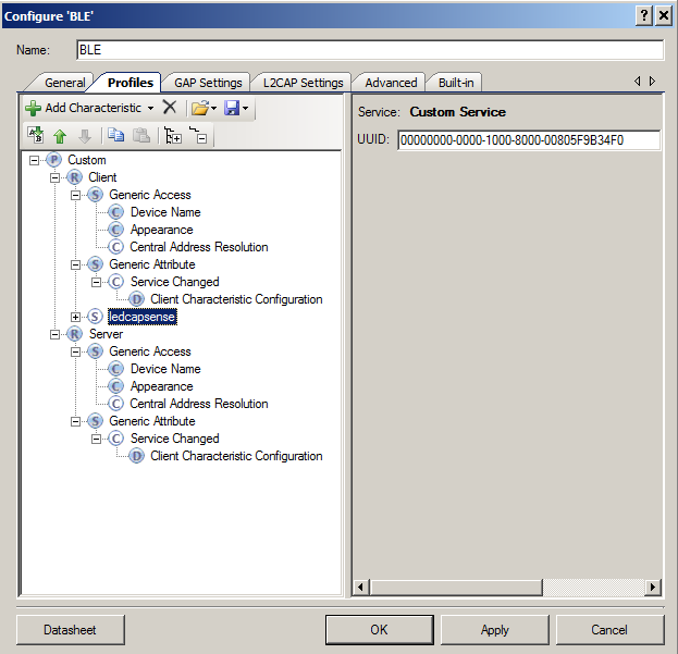
After all that you will end up with something that looks like this. You can see the “ledcapsense” service is listed under the “client” section of the GATT configuration.
PSoC4 BLE Central Firmware
The firmware for the PSoC4 BLE Central needs to:
Initialize the PSoC
Scan for GAP Peripherals that are advertising the “ledcapsense” service
Connect to the GAP Peripheral & Discover its services
Turn on notifications for the Capsense characteristic
Loop
If the users changes the state of the button then send over a LED on/off
If you receive a notification of a change in capsense then update the PWM Compare value (to change the intensity)
Most of the Cypress BLE APIs will create an “event” that you will need to process in the BLE loop. The interesting events are:
Event
Description
CYBLE_EVT_STACK_ON
The BLE Stack has turned on and you can start advertising
CYBLE_EVT_GAP_DEVICE_DISCONNECTED
The GAP Peripheral you were attached to has disconnected. Start scanning for another GAP Peripheral to attach to
CYBLE_EVT_GAP_DEVICE_CONNECTED
You have successfully completed a connection to a GAP Peripheral
CYBLE_EVT_GAPC_SCAN_PROGRESS_RESULT
You received an advertising packet from a GAP Peripheral
CYBLE_EVT_GAPC_SCAN_START_STOP
You either stopped or started scanning for advertising packets from GAP Peripherals
CYBLE_EVT_GATT_CONNECT_IND
The GATT Connection is complete. This event occurs before the CYBLE_EVT_GAP_DEVICE_CONNECTED EVENT so you don't need to do anything
CYBLE_EVT_GATTC_DISCOVERY_COMPLETE
The service discovery is complete. You can now set the CCCD and turn on the PWM
CYBLE_EVT_GATTC_HANDLE_VALUE_NTF
You received a notification of a change in the Capsense from the GAP Peripheral.
CYBLE_EVT_GATTC_WRITE_RSP:
Your write succeeded. For this application there is nothing to do
To make all of this work, I created a state machine using an enumerated datatype.
// Modes for a statemachine
typedef enum SystemMode {
    SM_INITIALIZE,          // Startup state
    SM_SCANNING,            // Looking for a Peripheral
    SM_CONNECTING,          // I have issued connected and waiting for it to complete
    SM_SERVICEDISCOVERY,    // Started the service discovery and waiting for it to complete
    SM_CONNECTED            // Connection complete...
} SystemMode_t;

static SystemMode_t systemMode = SM_INITIALIZE; // Starting mode of statemachine
1. Initialize the PSoC4 BLE Central
The project starts with the normal turn on the PSoC components and stuff.
int main(void)
{
    CyGlobalIntEnable; /* Enable global interrupts. */
    UART_Start();
    PWM_Start();
    CyBle_Start( CyBle_AppCallback );
2. Scan for Peripherals that are advertising the “ledcapsense” service
Most everything that happens in the BLE sub-system triggers a callback to your “AppCallback” which you registered when you started up the BLE component. The AppCallback has two parameters, which event and a generic void* style argument which can be one of a bunch of things.
(Lines 73-79) After you turn on the power to your central and the BLE subsystem you will need to start scanning for peripherals that are advertising. To do this you call “CyBle_GapcStartScan”. The “Gapc” part of the API name means GAP Central. The other time you need to start scanning is when you have been disconnected.
(Lines 81-93) When you receive an advertising packet you can look in the packet and figure out if it is a GAP Peripheral that you want to attach too. In this case I:
Only look at packets that are 29 bytes long (which I looked up in the BLE GAP Peripheral project)
And.. if the packet has the UUID of the capsenseled service
Then I save the Bluetooth Device Address (BD address) and stop scanning. When the scanning is stopped the BLE subsystem will issue and event called “CYBLE_EVT_GAPC_SCAN_START_STOP” (the next section)
       case CYBLE_EVT_STACK_ON:
        case CYBLE_EVT_GAP_DEVICE_DISCONNECTED:
            systemMode = SM_SCANNING;
            enabledCapsenseNotifications = 0;
            CyBle_GapcStartScan(CYBLE_SCANNING_FAST); // Start scanning for peripherals
            PWM_WriteCompare(0); PWM_Stop();          // Turn off the LED
        break;

        CYBLE_GAPC_ADV_REPORT_T* scanReport;
        case CYBLE_EVT_GAPC_SCAN_PROGRESS_RESULT:                     // Advertising packet
            scanReport = (CYBLE_GAPC_ADV_REPORT_T*)eventParam;
            if(scanReport->dataLen != 29)                             // Number of bytes in ledcapsense advertising packet
                break;
            if(memcmp(&CapLedService,&scanReport->data[11],sizeof(CapLedService))) // if service is in packet
                return;

            // Setup for the connection
            remoteDevice.type = scanReport->peerAddrType;          // setup the BD addr
            memcpy(&remoteDevice.bdAddr,scanReport->peerBdAddr,6); // 6 bytes in BD addr
            systemMode = SM_CONNECTING;
            CyBle_GapcStopScan();                                  // stop scanning for peripherals

        break;
3. Connect to the Peripheral & Discover the Services
(lines 97-100) When the BLE either starts or stops scanning it issues the “CYBLE_EVT_GAPC_SCAN_START_STOP” event. I use the state machine to determine what to do. Basically if the mode of my system is “SM_CONNECTING” then I attempt to make a connection to the remote device.
(lines 102-105) Once the device is connected you need to do a service discovery to find out what services are on the GAP Peripheral and more importantly what are the handles of the characteristics. The CyBle_GattcStartDiscovery issues requests to the GAP Peripheral to tell the services and characteristics on the peripheral, to which it responds with events. Cypress provides code in BLE_custom.h and BLE_custom.c to process those responses. Once the discovery is complete you are then ready to talk to the device.
        case CYBLE_EVT_GAPC_SCAN_START_STOP: // If you stopped scanning to make a connection.. then launch connection
            if(systemMode == SM_CONNECTING )
                CyBle_GapcConnectDevice(&remoteDevice);
        break;

        case CYBLE_EVT_GAP_DEVICE_CONNECTED:              // Connection request is complete
            CyBle_GattcStartDiscovery(cyBle_connHandle);  // Discover the services on the GATT Server
            systemMode = SM_SERVICEDISCOVERY;
        break;
4. Turn on notifications for the Capsense characteristic
We are interested in getting notified when the Capsense characteristic on the GAP Peripheral changes. To enable getting a notification you need to write a “0x01” into the Client Characteristic Configuration Descriptor or CCCD. In order to accomplish this you need to know the handle of that descriptor. The handle is discovered automatically by the BLE_custom.c functions. If you look in BLE_custom.h you will find #define(s) that are the indexes of the things you need to know from the service discovery array.
/* Below are the indexes and handles of the defined Custom Services and their characteristics */
#define CYBLE_CUSTOMC_LEDCAPSENSE_SERVICE_INDEX   (0x00u) /* Index of ledcapsense service in the cyBle_customCServ array */
#define CYBLE_CUSTOMC_LEDCAPSENSE_LED_CHAR_INDEX   (0x00u) /* Index of led characteristic */
#define CYBLE_CUSTOMC_LEDCAPSENSE_LED_CHARACTERISTIC_USER_DESCRIPTION_DESC_INDEX   (0x00u) /* Index of Characteristic User Description descriptor */
#define CYBLE_CUSTOMC_LEDCAPSENSE_CAPSENSE_CHAR_INDEX   (0x01u) /* Index of capsense characteristic */
#define CYBLE_CUSTOMC_LEDCAPSENSE_CAPSENSE_CAPSENSECCCD_DESC_INDEX   (0x00u) /* Index of capsensecccd descriptor */
#define CYBLE_CUSTOMC_LEDCAPSENSE_CAPSENSE_CHARACTERISTIC_USER_DESCRIPTION_DESC_INDEX   (0x01u) /* Index of Characteristic User Description descriptor */
To set the CCCD you create a “CYBLE_GATTC_WRITE_REQ_T” and fill it in with the information required. Specifically, the value and the handle which you find on line 57. Then you write it to the GAP Peripheral.
/***************************************************************
 * Function to set the Capsense CCCD to get notifications
 **************************************************************/
void updateCapsenseNotification()
{
    CYBLE_GATTC_WRITE_REQ_T 	tempHandle;
    uint8 cccd=1;
    enabledCapsenseNotifications = 1;

    tempHandle.attrHandle = cyBle_customCServ[CYBLE_CUSTOMC_LEDCAPSENSE_SERVICE_INDEX]
    .customServChar[CYBLE_CUSTOMC_LEDCAPSENSE_CAPSENSE_CHAR_INDEX]
    .customServCharDesc[CYBLE_CUSTOMC_LEDCAPSENSE_CAPSENSE_CAPSENSECCCD_DESC_INDEX].descHandle;

  	tempHandle.value.val = (uint8 *) &cccd;
    tempHandle.value.len = 1;

    CyBle_GattcWriteCharacteristicValue(cyBle_connHandle,&tempHandle);
}
5. Main Loop
The main look is simple. Basically if you are in the SM_CONNECTED state, then call the function which updates the state of the Remote LED.
   for(;;)
    {
        switch(systemMode)
        {
            case SM_INITIALIZE:
            case SM_SCANNING:
            case SM_CONNECTING:
            case SM_SERVICEDISCOVERY:
            break;
            case SM_CONNECTED:
                updateLed();
            break;
        }

        CyBle_ProcessEvents();
        CyBle_EnterLPM(CYBLE_BLESS_DEEPSLEEP);
    }
}
5. Main Loop (Write the state of the LED)
This function looks at the state of the switch, then if it has changed, sends the updates state to the Peripheral. The switch is active low (a 0 means that it is pressed) but we want a “1” to mean turn on the LED.
Just like the updateCapsenseNotification() function, you look in the cycle_customCServ array to find the handle of the LED characteristic.
/***************************************************************
 * Function to update the LED state in the GATT database
 * Based on state of swtich
 **************************************************************/
void updateLed()
{
    static int previousState = 10;       // The first time it is called send the data
    uint8 state;                         // A place to hold the state of the switch
    CYBLE_GATTC_WRITE_REQ_T tempHandle;  // A handle to call the BLE API

    state = !SW1_Read();                 // Active low switch
    if(state == previousState)           // If nothing has changed dont send anythign
        return;

    previousState = state;
    tempHandle.attrHandle = cyBle_customCServ[CYBLE_CUSTOMC_LEDCAPSENSE_SERVICE_INDEX]
        .customServChar[CYBLE_CUSTOMC_LEDCAPSENSE_LED_CHAR_INDEX]
        .customServCharHandle;

  	tempHandle.value.val = (uint8 *) &state;
    tempHandle.value.len = 1;

    CyBle_GattcWriteCharacteristicValue(cyBle_connHandle,&tempHandle);
}
5. Main Loop (Capsense Notifications)
The last bit of code updates the state of the PWM driving the LED when you get a notification from the GAP Peripheral that it has been updated.
        CYBLE_GATTC_HANDLE_VALUE_NTF_PARAM_T *capsenseNTF;
        case CYBLE_EVT_GATTC_HANDLE_VALUE_NTF:                                 // Capsense Notification Recevied
            capsenseNTF = (CYBLE_GATTC_HANDLE_VALUE_NTF_PARAM_T *)eventParam;
            if(capsenseNTF->handleValPair.value.val[0] == 0xFF)                // Turn off the LED in no touch
                PWM_WriteCompare(0);
            else
                PWM_WriteCompare(capsenseNTF->handleValPair.value.val[0]);
        break;

        case CYBLE_EVT_GATTC_WRITE_RSP: // Sucesfull write - nothing to do
        break;
In the next Article(s) I will show you how to use the CySmart dongle. I am also planning on showing you the firmware to create a GATT Browser.
In the previous Pinball post, I wrote about getting the OLED going and getting the footprint onto my printed circuit board. Now I need to make PSoC firmware to drive the display. I turns out that there are a number of different driver chips out there including at least SSD1306, SH1106, LD7032, SSD1325, and ST7920 that handle multiplexing the columns/rows, managing frame buffers, power management, etc. To make matters more fun, these chips support I2C, 3&4 wire SPI and a couple of different parallel interfaces (6800, 8080). I certainly didn’t want to go down the rathole of building up a complete driver library. But I didn’t have to, as it turns out that that Oliver Kraus built and open-sourced a very nice library that you can get at www.github.com/olikraus/u8g2. This library (and its predecessor u8glib) seem to be in pretty wide use in Arduino and Raspberry Pi.
In order to make the library work with the PSoC I had to do several things
Download it from GitHub (git clone git@github.com:olikraus/u8g2.git)
Created a new PSoC4200M project for the CY8CKIT-044 (which was the devkit that I happened to have sitting next to my computer)
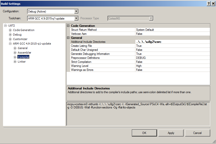
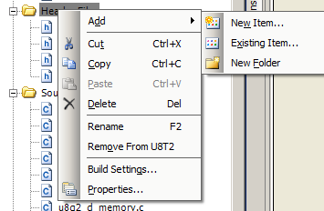
Change the build settings (right click on the project and select building settings) then add the directory in “Additional Include Directories” and include the “u8g2/csrc” directory.
Add the header files to the project by right clicking and selecting “Add->Existing item” so that the project can f
Add the U8G2 C-Files to the project (same as step 4 but add the C files)
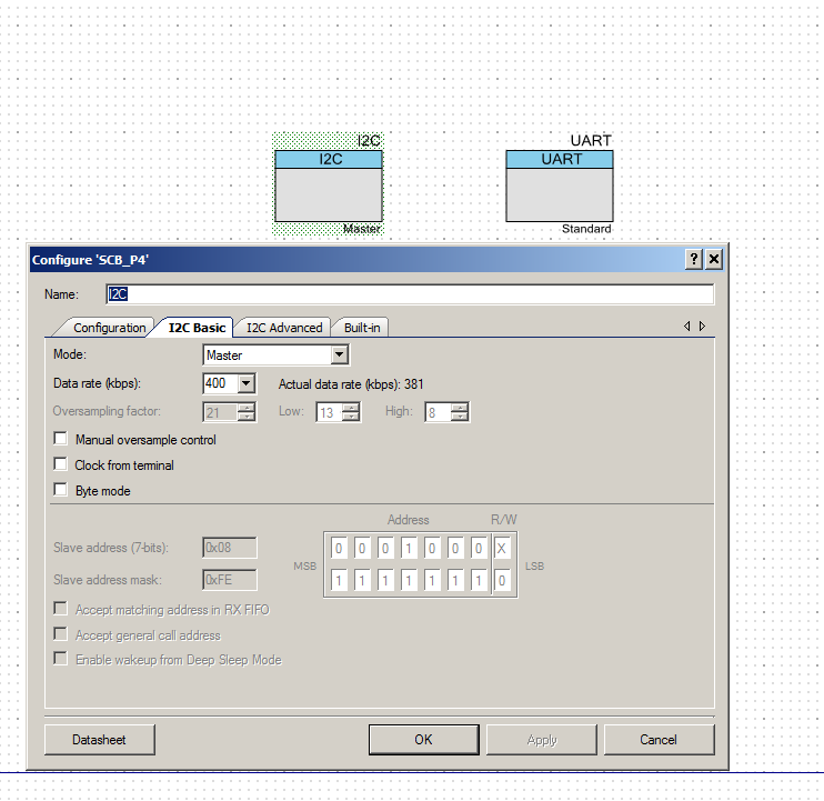
Build a schematic which has an I2C (for the display) and a debugging UART. The I2C is configured as a master with 400kbs data rate. The UART uses the default configuration.
Assign the pins
Now I am ready to build some firmware that will drive the display. In order to use the library with a PSoC I need to create two functions for the U8G2 HAL to use as an interface to the PSoC hardware. You initialize the U8G2 system with a call to the u8x8_Setup function. In that call you need to provide function pointers too the two HAL functions
The GPIO and Delay Interface
The byte oriented communication interface
This is an example of the setup required:
The GPIO and Delay interface is used by the byte oriented communication functions to read/write the GPIOs and provide delays. This function provides the underpinnings of a bit-banged I2C, UART, SPI etc. Because I am only going to use PSoC Hardware to provide the I2C interface I will only respond to the delay messages. All of the delay functions are implemented as busy wait loops, which I am not a big fan of. The input to the function is a “message” that is one of a sprawling list of #defines in the file u8x8.h. I believe that I found all of the possible cases, but I am not sure.
The first message, UX8X8_MSG_GPIO_AND_DELAY_INIT doesnt need to do anything because the GPIOs are configured correctly by the default.
I did not respond to the messages of the form U8X8_MSG_GPIO_X which are the read and write of the GPIOs as I am not going to use the bit-banged interface.
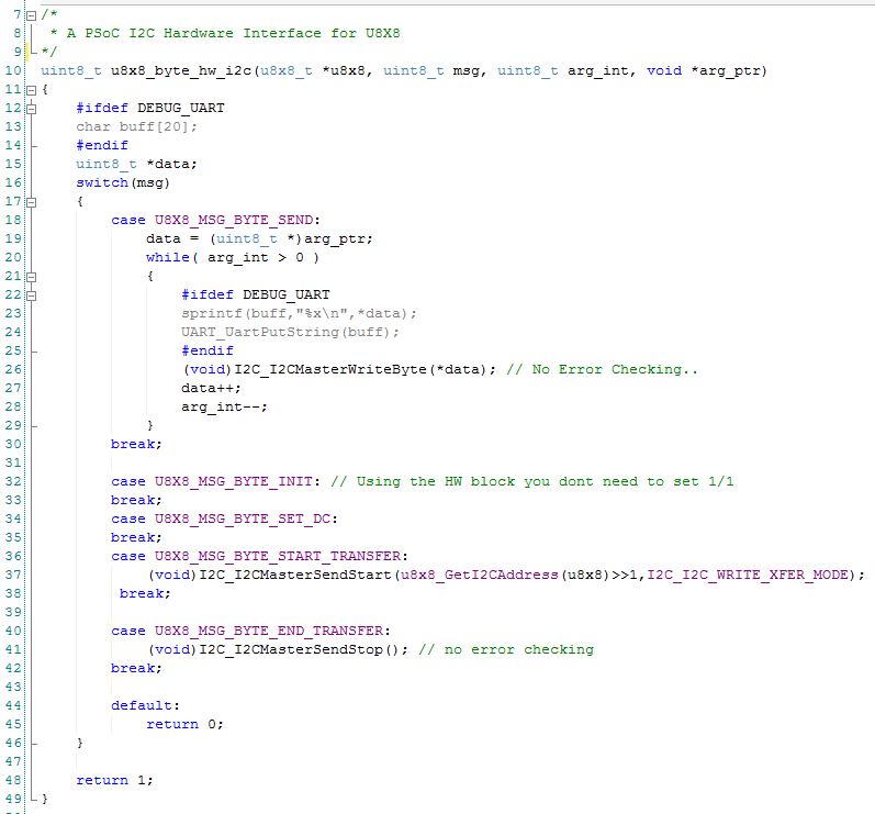
The other function that needs to be provided is the byte-oriented communication function. This function needs to respond to the messages to start, send, and end communication. I just mapped those messages onto the PSoC hardware APIs. While I was trying to understand what was happening with the system I implemented a debugging UART which you can see in the #ifdef DEBUG_UART sections.
You can find all of the source code and files at the IOTEXPERT site on github.
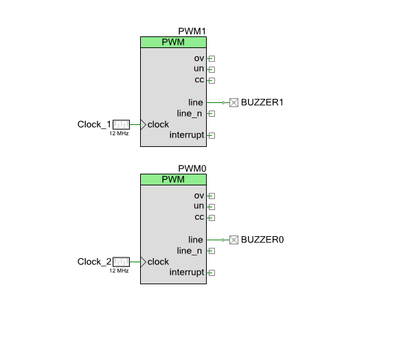
After a few days off (Im sorry) I am back to it. Every Pinball machine does lots of beeping, buzzing and music playing as will this one. A very inexpensive way to make sound is to use a piezo-electric buzzer. To make it “buzz”, you just drive a 50% duty cycle square wave into it at the frequency you want. This is a perfect task for the PSoC4 BLE Timer Counter Pulse Width Modulator (TCPWM). There are obviously limitations with this scheme, starting with you can only play one note at a time, and the notes can only be square (real sound has a much more complex waveforms). But all of that is OK because the buzzer work OK and, as I said… they are cheap. On the Pinball printed circuit board I have placed two buzzers, my thought was one would be used for buzzing and one would be used to play a song.
To make things easier for the main firmware I will build a component just like I did for the LEDs and the Switches. Start by creating a new component by:
Click on the components tab
Right click on the “Pinball Component” library project and select “Add Component Item…”
Select “Symbol Wizard”, give the component the name “MusicPlayer” (exactly like I did in the LED and Switches components)
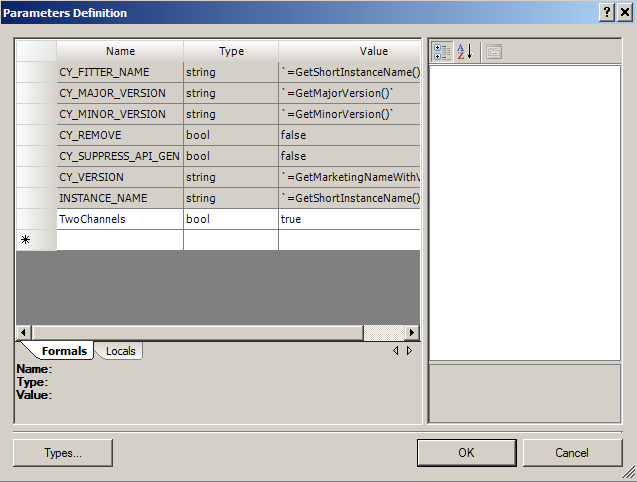
I thought that it would be nice for the MusicPlayer component to be able to select if it is a one or two channel player. So, right click on the blank part of the symbol editor canvas and select “Symbol Parameters”. Next add a bool parameter called “TwoChannels”
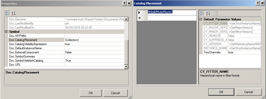
To put the component in the correct place in the Component Browser right click the blank canvas, select “edit properties”, edit the”Doc.CatalogPlacement” and enter the placement of “Pinball/MusicPlayer/”
Next, you need to create the schematic for the music player. You do this by right-clicking on the “Pinball Component” project and adding a “Schematic” implementation. Then add the default clocks, the TCPWMs and the pins.
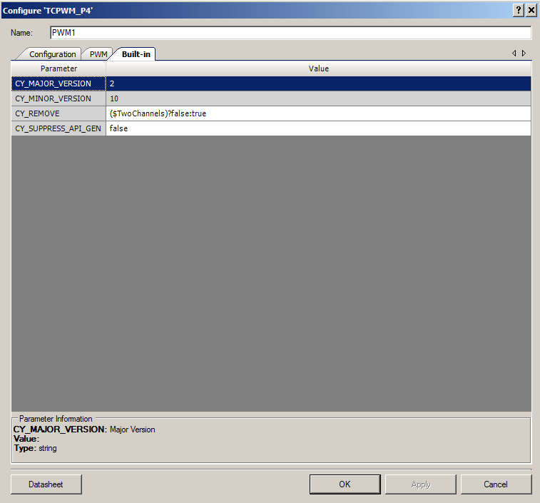
Earlier I added a component parameter called “TwoChannels”. When this parameter is false, I want to remove the extra components. With the help of the Cypress component manager I found out how to do this. And it is simple. Just add an expression to the TCPWM, Pin and Clock “CY_REMOVE” Parameter. This parameter shows up on the “Built-in” tab for these three components (in fact all Cypress components). When the value is “true” the component magically disappears.
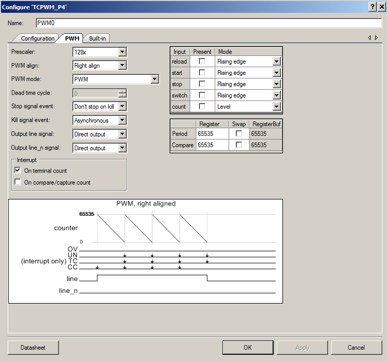
Next, I configure the TCPWM to have the prescaler turned on (which divides the input clock). This is used to reduce the default 12MHz clock down to an easier to control 93.75Khz.
In the next post Ill show you the firmware.
You can find all of the source code and files at the IOTEXPERT site on github.


 After that I can Read and Write attributes (like the LED Attribute) by typing the value I want to write into the box on the upper right, and pressing “Write Value”. For example you can turn on the LED by writing a “1” into the LED characteristic.
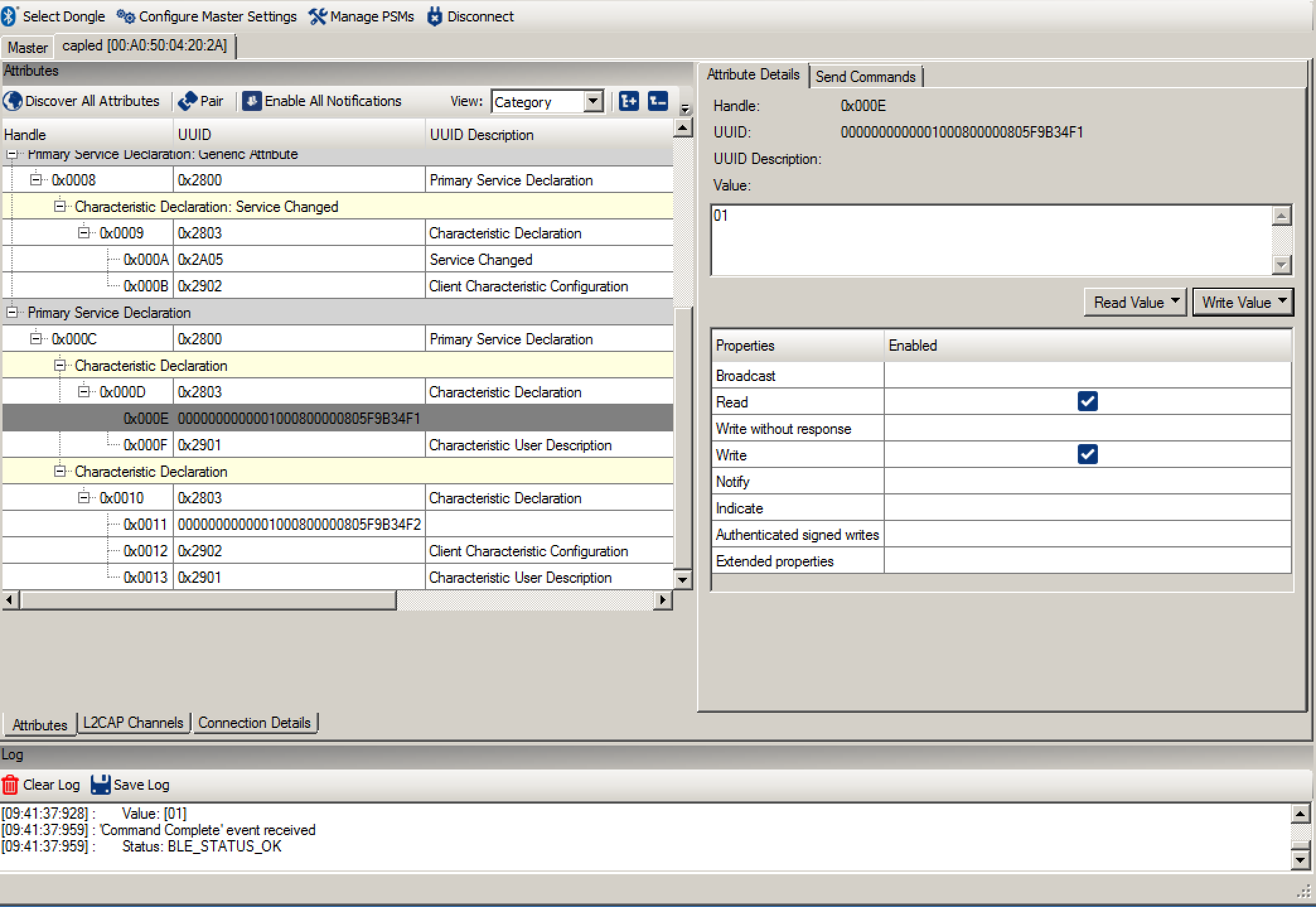


