ThingSoC PSoC4L: Using & Debugging the PSoC4 Clock

Pattern Agents are running a crowd funding effort for TSoC … here

Summary

In the previous post I told you that I immediately blew away the factory firmware on the TSoC4L board.  I’m like that sometimes :-).  In this post I am going to take you through the entire process of getting and reprogramming the factory firmware, then finding and debugging a PSoC4 clock problem.  The rest of this post is:

  1. Getting the correct firmware back on the TSoC4L Board
  2. Running into a bug in the beta version of the firmware
  3. Using the debugger to find the bug
  4. Explaining the functionality of Low Frequency Clocks and the Watch Dog Timer
  5. The Pattern Agents bug fix

Factory Firmware

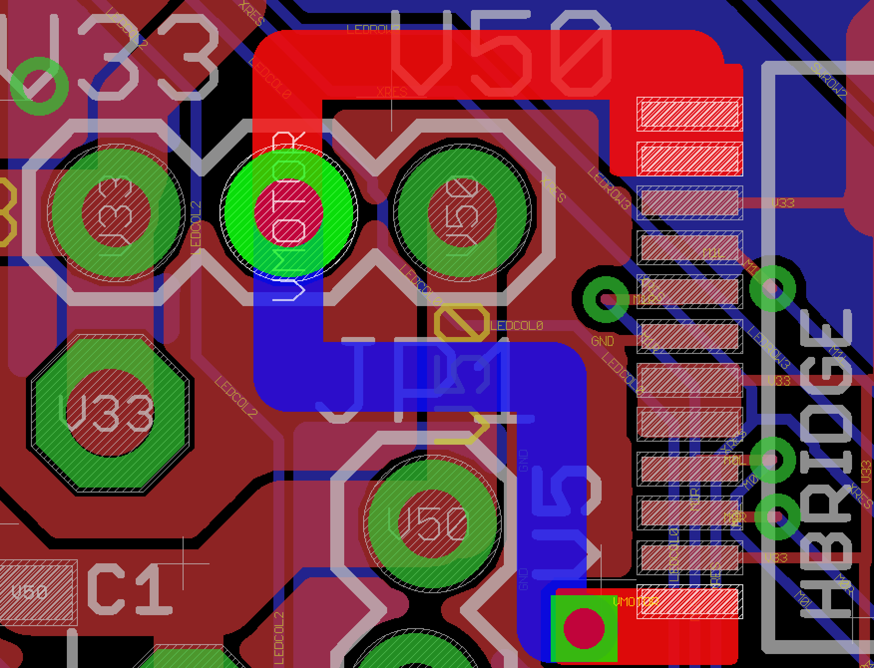
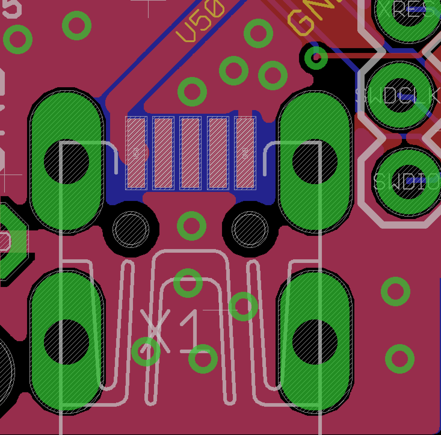
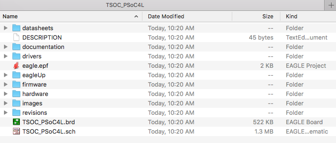
Getting things going again starts with “git”ing the firmware.  This can be done by “git clone git@github.com:PatternAgents/TSOC_PSoC4L.git”.  Once you have the repo cloned you will find a bunch of good stuff including:

  1. datasheets: All the datasheets
  2. documentation: The PatternAgents documentation (quick start)
  3. drivers: The windows USB <-> UART drivers
  4. eagleUp: JPG renderings of the PCB
  5. firmware: The PSoC Creator Project
  6. hardware: gerbers, boms etc
  7. images: renderings of the board, photos of the board etc
  8. revisions: old revisions of the Eagle project files
  9. The Eagle PCB Project including schematic and layout

TSoC4 L Files from GitHub

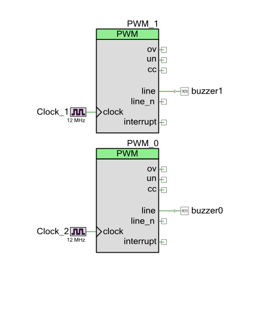
When you open the PSoC Creator Workspace you will find two projects

  1. A USB Bootloader – called “USBFS_Bootloader”
  2. The TSoC RSVP Firmware – called “rspvsis_4l_typ”

The system is supposed to

  1. Start the USB HID bootloader (so you could get new firmware).  Wait for 10 seconds for a bootloader host to start then if it doesnt … then start
  2. The RSVP Firmware

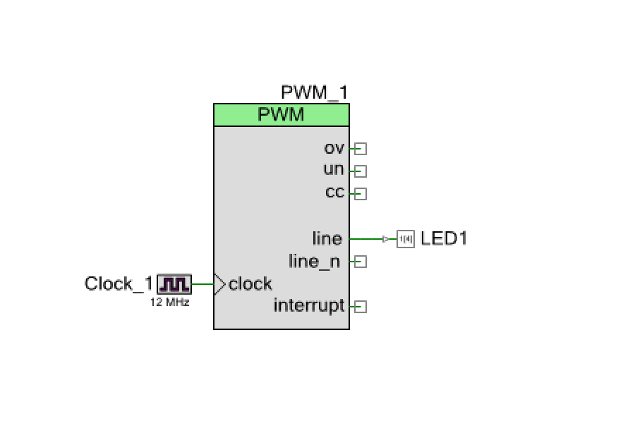
When you plug in the board you will see the TSoC4L enumerate as “Cypress ThingSoc Bootloader”.  Then, after 10 seconds, you should see it reboot, then enumerate as “Cypress USB UART”.  But, this was not happening for me.  Why?  I wasn’t sure.  The first thing that I did was add a blinking LED circuit that looked like this:

Blinking LED

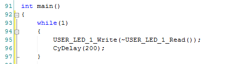
But the LED was not blinking.  That meant that the firmware was not even getting to main i.e. it was hanging BEFORE main in the PSoC boot code.  But where and why?

Using the Debugger to Find the Bug

How do you figure out where the system is stuck if you can’t even use the “blinking LED” or “printf” debug?  Simple.  Use the debugger.  Start by programming the PSoC with your firmware.  Then click “Debug->Attach to running target”.

Starting the PSoC Debugger

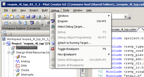
The debugger will start.  Then you will be able to press the “Pause” button. which will take you to a screen that looks like this:

PSoC4 Clock Busy Wait Loop

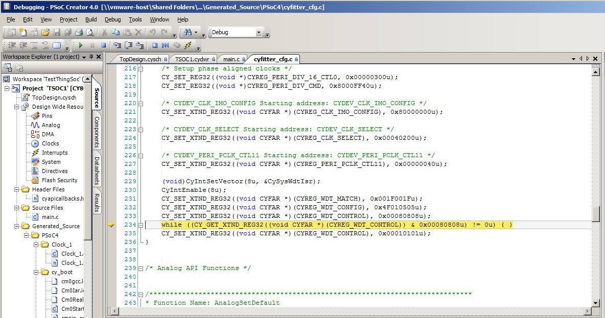
The chip is stuck on line 234.  What does line 234 do?  That is a busy wait loop.  It is waiting for the Watch Dog Control Register to clear.  To explain that, I will need to take you through the PSoC4 Low Frequency Clocks.  First you should notice that the file we are in is named “cyfitter_cfg.c”.  What is this file?  If you look at the top, this is what PSoC Creator says.

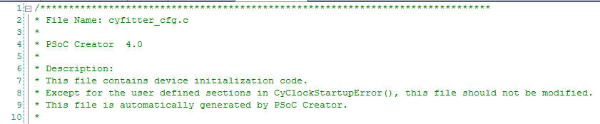
This means that the “cyfitter_cfg.c” file is synthesized by PSoC Creator when you do a build based on what you configured when you setup your project.  This file contains a bunch of the startup code including the code that gets the clock systems going.  Line 234 is inside of a function called “ClockSetup”.  All of this code is called BEFORE you get to main().

The PSoC4 Clock(s)

To explain why we are stuck there you first need to double click on the “Clocks” tab in the Design Wide Resources.  When you do that it will take you to this screen which contains a bunch of information about the clocking system in the PSoC.

PSoC4 Clock Setup

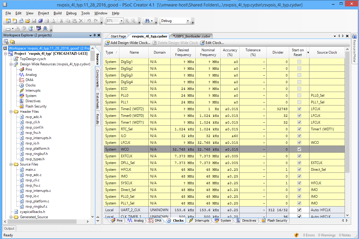
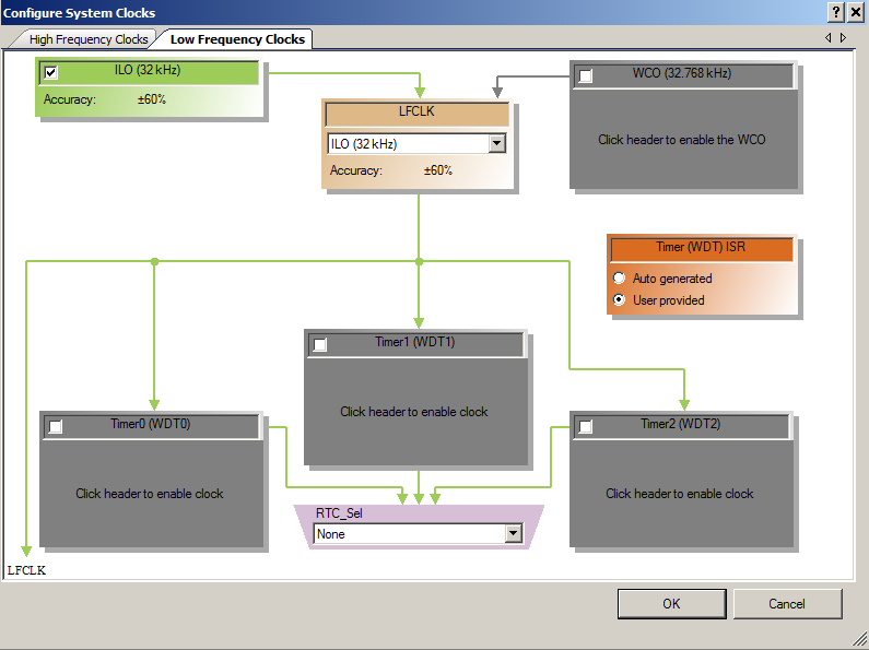
In the screen above, you can see that there are three Timers in the Watch Dog Timer system (WDT) that are clocked (i.e. have a Source Clock of) by the Low Frequency Clock (LFCLK).  The LFCLK has its source as the Watch Crystal Oscillator (WCO).  If you double click the WCO line it will take you to a screen that is much easier to see what is going on, specifically the “Configure System Clocks” screen:

PSoC4 Clock - Low Frequency

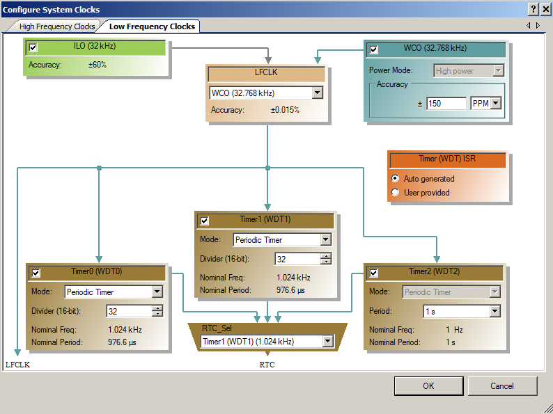
In the screen above you can see that the LFCLK has two choices of oscillator sources, the “ILO” or the “WCO”.  ILO stands for Internal Low Speed Oscillator.  The ILO is a fairly inaccurate (+- 60%) RC oscillator that is built inside of the chip.   It is designed to be very low power which is why it is so inaccurate.  If you need a more accurate oscillator, then you should use an external oscillator, specifically a Watch Crystal Oscillator or WCO.  A WCO is a 32.768KHz crystal oscillator.  These watch crystal oscillators give you very precise clocks that can be used to drive real time clocks accurately.

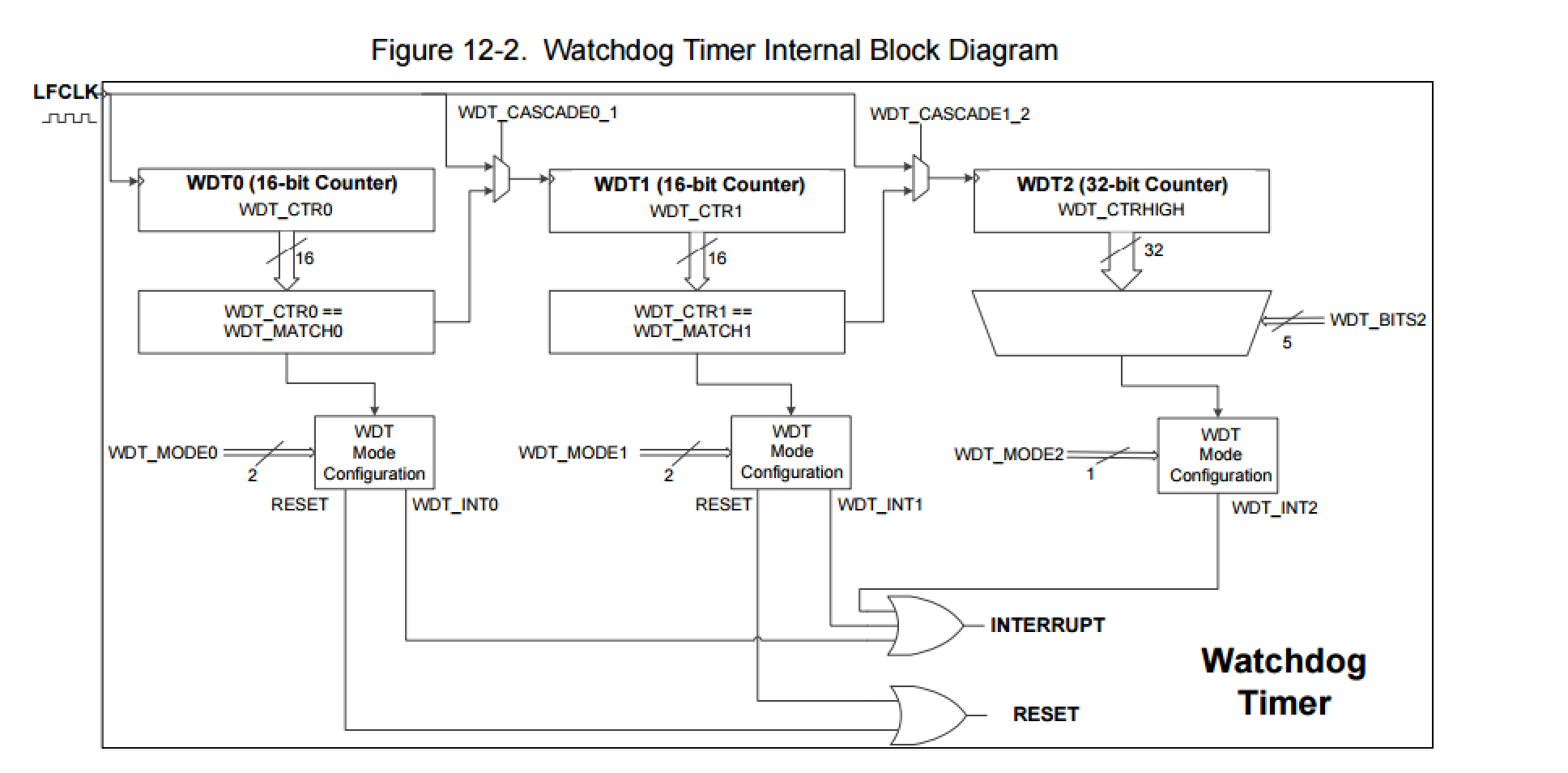
The next thing to see is there are three Watch Dog Timers (WDT) numbered 0-2.  These times are driven by the “LFCLK”.  Here is a picture from the PSoC Technical Reference Manual.


PSoC4 Clock - WDT Block Diagram

So what is the “CYREG_WDT_CONTROL”?  You can find that by looking in the PSoC4 Registers TRM.

PSoC4 Clock WDT Control Register

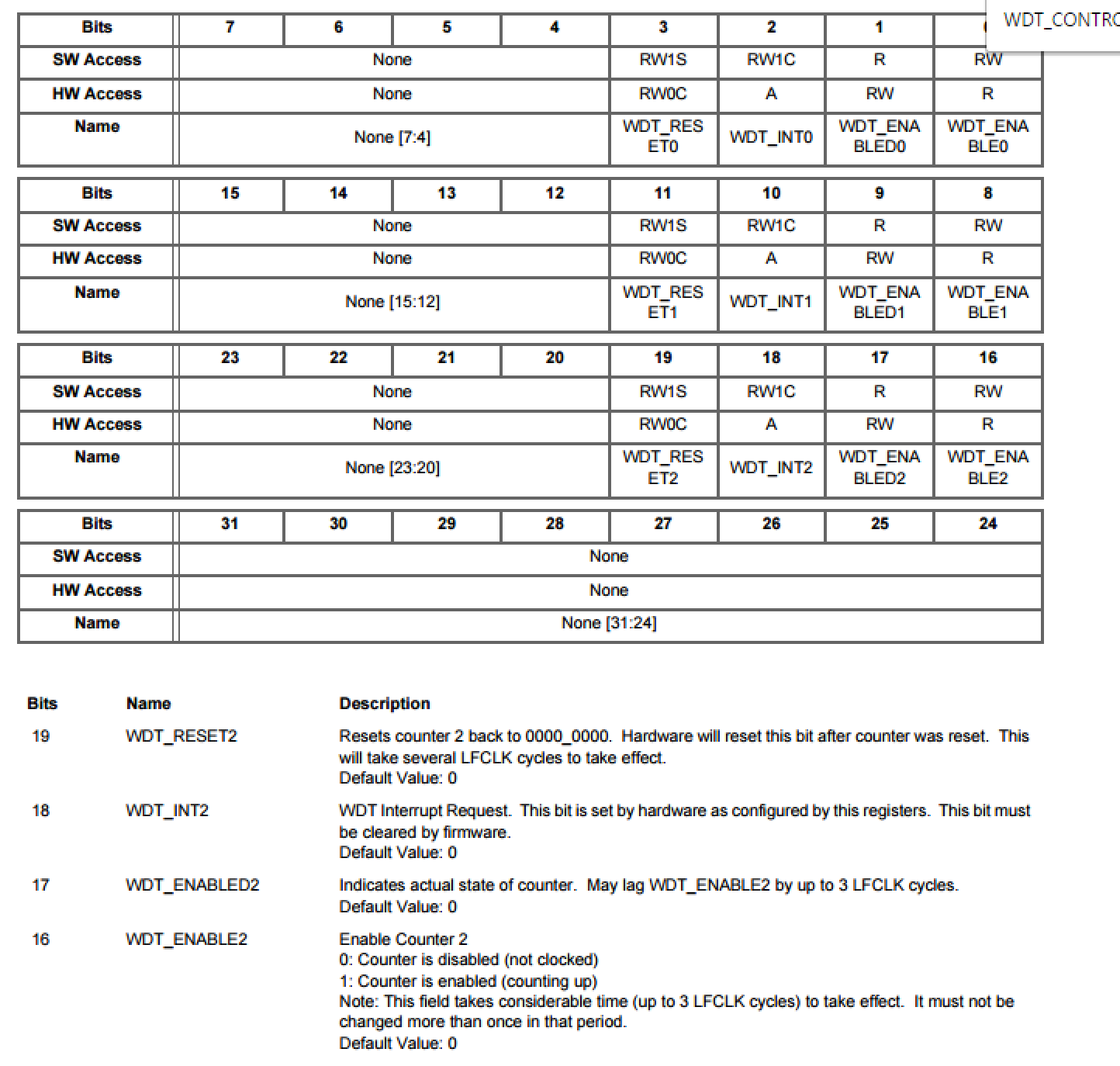
The busy wait loop is waiting for bits 19,11,3 to be cleared.  Those bits are “WDT_RESETx”  They become 0 when the three WDT timers are cleared which happens “several LFCLK cycles” after the reset.  As a reminder, here is that block of code:

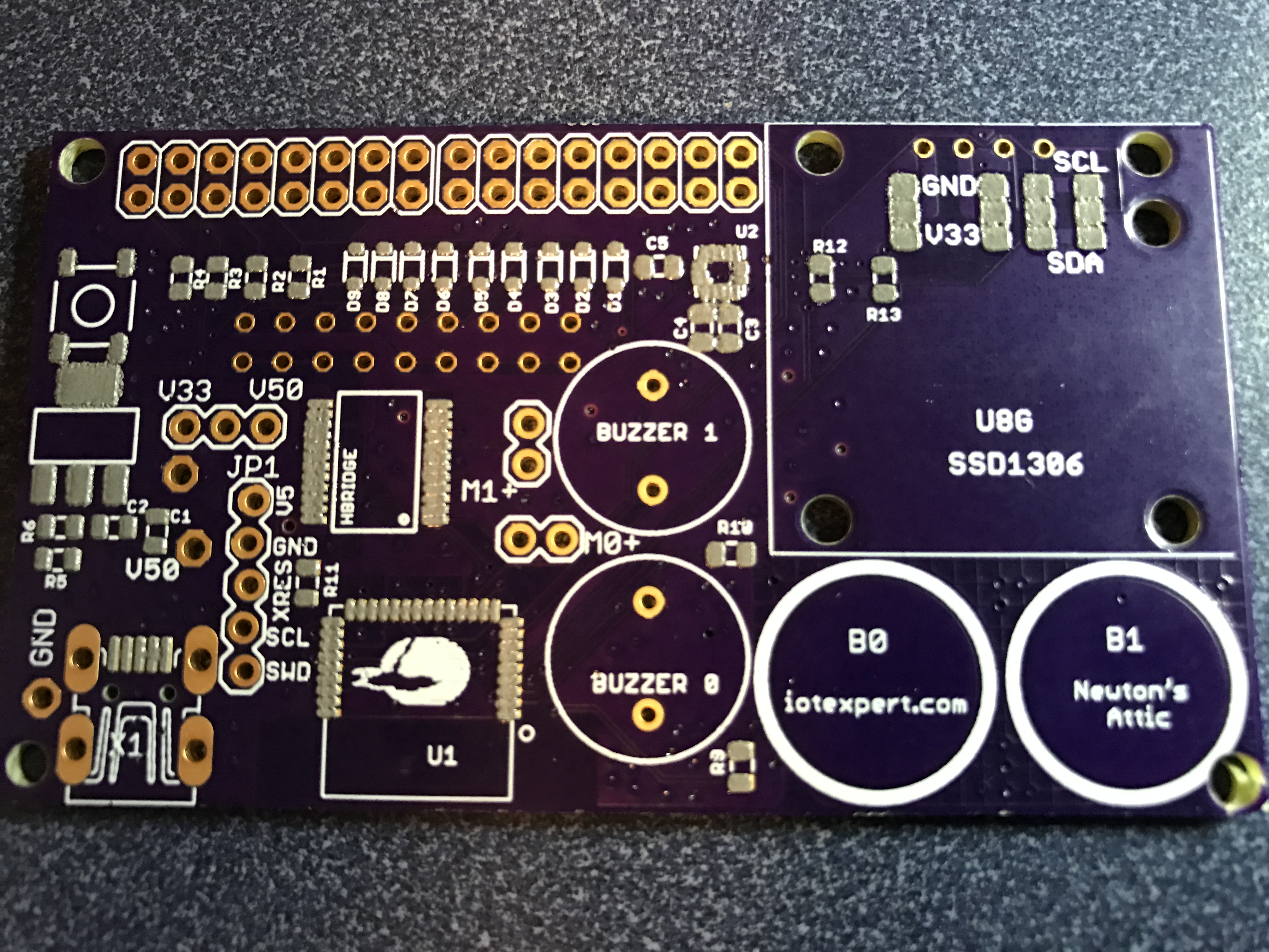
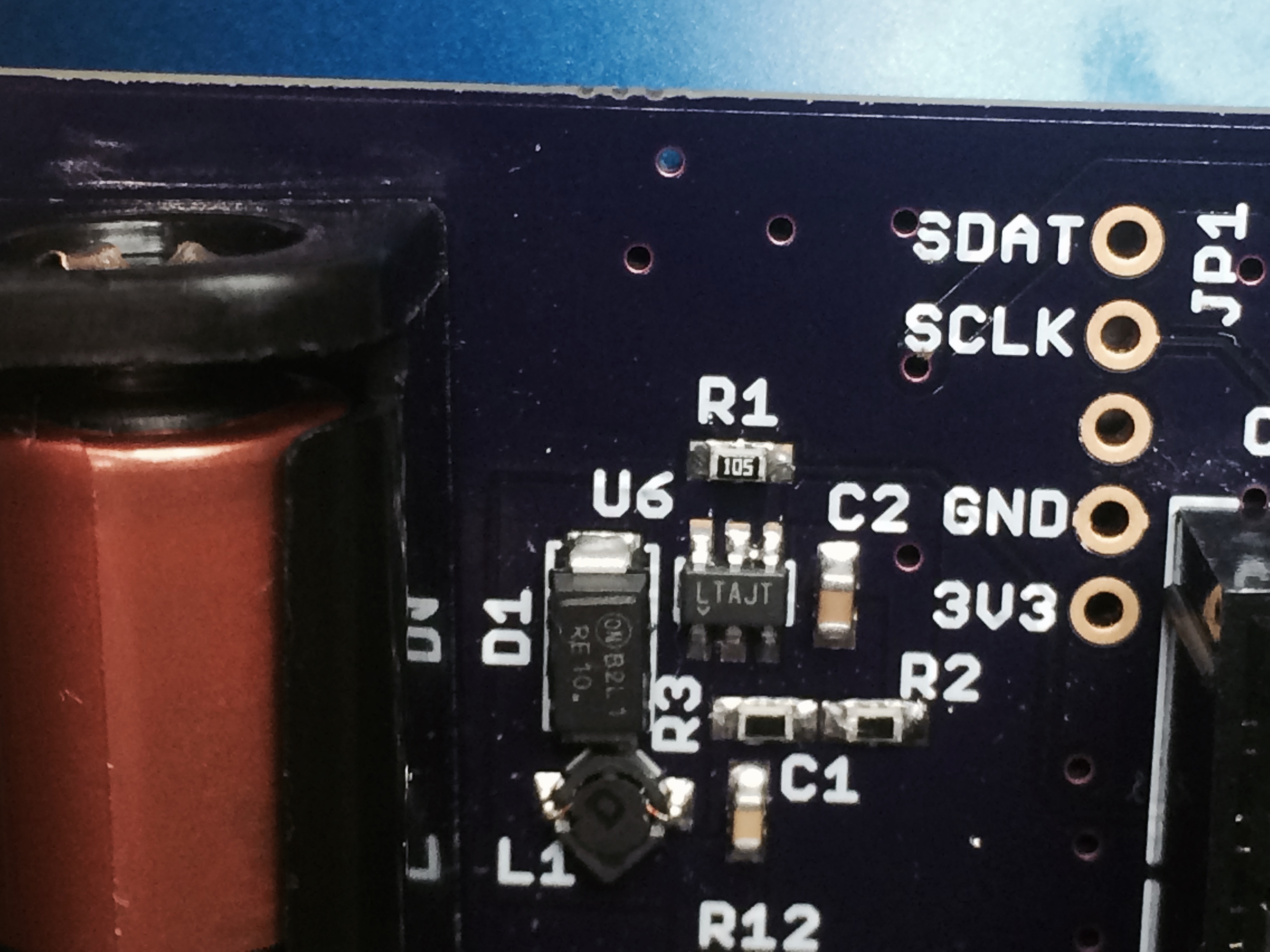
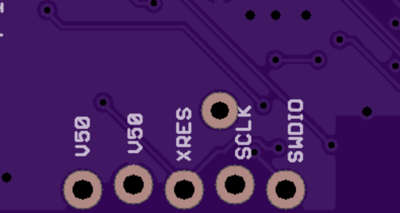
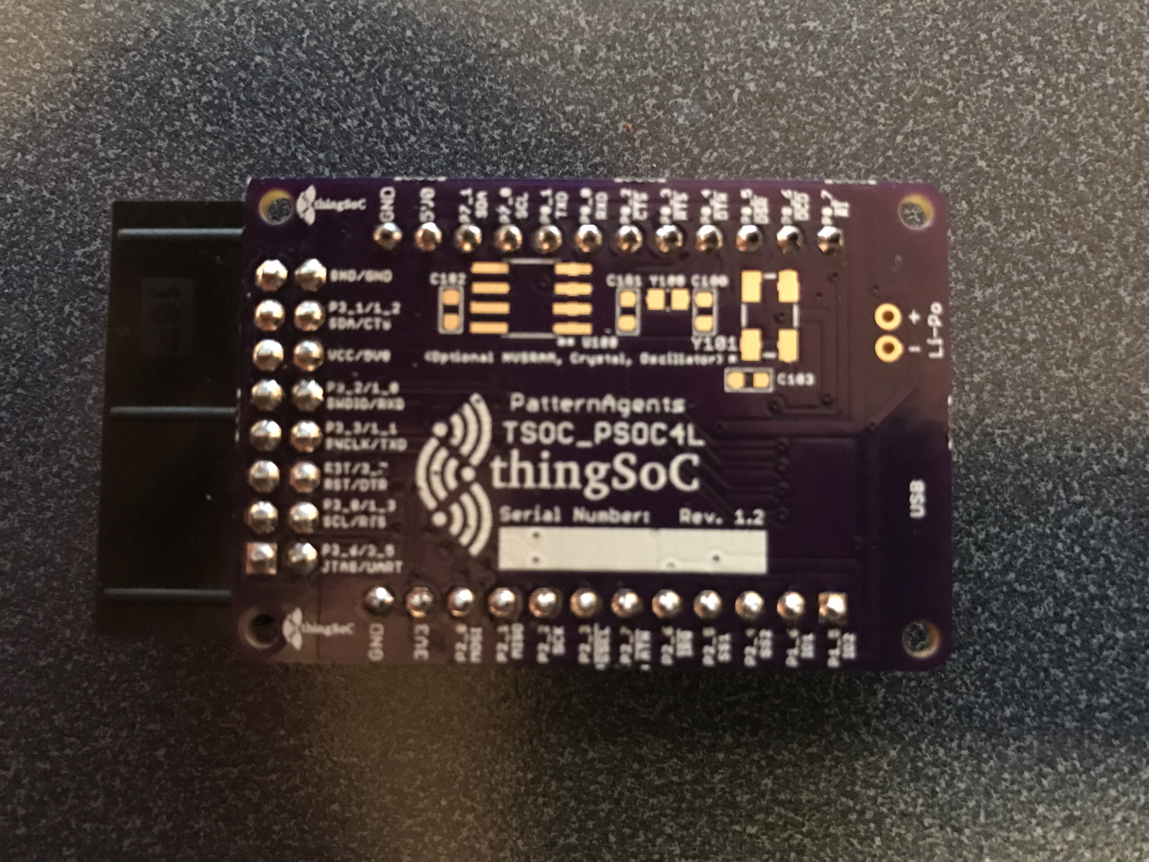
This still leaves us with the question, “What is the problem?”.  If you look on the back of the ThingSoC4L board you will see there is no Crystal populated on this board. (the blank footprint on the right side of the back).  The WCO is an optional feature from Pattern Agents.  If you need the more accurate timing, you need to solder on your own Crystal.

Backside of ThingSoC4L PCB

If there is no WCO crystal, then the WDT timer reset will never happen because LFCLK isn’t doing anything.  And, the busy wait loop will never end.  Mystery solved.

The Pattern Agents Bug Fix

To fix the startup problem, the Pattern Agents guys changed the clock configuration to

  1. Turn off the WDTs
  2. Use the ILO as the source of the LFCLK

PSoC4 Clock - Low Frequency Setup

You can find all of the projects in the TSoC Series at my GitHub ThingSoC repository git@github.com:iotexpert/ThingSoC.git

Index Description
ThingSoc: TSoC PSoC4L Development Kit from PatternAgents Introduction to ThingSoC
ThingSoC PSoC4L: Using & Debugging the PSoC4 Clock Debugging a beta firmware problem
ThingSoC: The TSoC GROVEY I2CHUB : I2C Hub/Switch Evaluating the ThingSoC I2C Hub
ThingSoC: Multiple I2C Displays Using the I2CHUB and U8X8 Library A project using ThingSoC I2C Hub & 4 OLED Displays

ThingSoC: TSoC PSoC4L Development Kit from PatternAgents

Pattern Agents are running a crowd funding effort for ThingSoC TSoC4L … help them here

Summary

Last week I got a box in the mail from my friend Tom Moxon in Oregon.  He runs a company called Pattern Agents.  I was excited when I saw the box because I love new development kits.  I was even more happy when I opened the box and found a ThingSoC PSoC4L kit.

Tom sent me three boards

  1. A ThingSoC PSoC4L
  2. A MiniProg Adaptor
  3. A ThingSoC I2C Hub

ThingSoC PSoC 4L Packaging

ThingSoC PSoC4L

The ThingSoC complies to a new open source stackable footprint called the ThingSoC Open Source Socket.  This ThingSoC board is driven by a PSoC4L.  The PSoC4L is the largest and most capable of the PSoC4 family.  This chip “completed” the high end of the PSoC4 family by adding more IOs, more Flash, more RAM and a USB controller.  The PSoC4L serves as the base MCU in the stack as well as providing a bridge to the PC via a USB <–> UART Connection.  The board also has a connection for a 3.7V LiPo battery to power the system.  In the picture below you can see the base board (on the left) with the programmer attachment (on the right).  The programmer attachment lets you attach a MiniProg-3 or a Uart Bridge or an ISSP connection (like a MiniProg-1).

thingsoc 4200l

Here is a picture of the backs of the boards.  On the back of the ThingSoC PSoC4L board you can see a place to solder a Cypress NVSRAM as well as a footprint for a Watch Crystal.

The backs of the ThingSoC PSoC4L

The Blinking LED

The first thing I did with the board (and no, reading the instructions wasn’t the first thing) was program the chip to blink the LED.  Obviously with a PSoC the best thing to do was make a schematic with a PWM driving the USER LED pin:

I used the default clock of 12MHZ, then I used the PWM pre divider to get the frequency down to something that I could see.

Lastly, I wrote a tiny bit of firmware to get things going.  Notice that I use the CySysPmSleep to put the CPU to sleep.  It never wakes up from this sleep (because there are no interrupt sources to wake it up).  But, if it did, it would go right back to sleep because of the loop.

After programming the board, the LED started right up.  That is good as it means everything makes sense.

When I programmed the Blinking LED project I overwrote Tom’s default firmware which is called “RISC”.  In the next post Ill talk more about the architecture of the ThingSoC PSoC4L.

You can find all of the projects in the TSoC Series at my GitHub ThingSoC repository git@github.com:iotexpert/ThingSoC.git

Index Description
ThingSoc: TSoC PSoC4L Development Kit from PatternAgents Introduction to ThingSoC
ThingSoC PSoC4L: Using & Debugging the PSoC4 Clock Debugging a beta firmware problem
ThingSoC: The TSoC GROVEY I2CHUB : I2C Hub/Switch Evaluating the ThingSoC I2C Hub
ThingSoC: Multiple I2C Displays Using the I2CHUB and U8X8 Library A project using ThingSoC I2C Hub & 4 OLED Displays

Pinball: Testing the Eagle PCB

Summary

In the previous post I talked about my process for assembling the Pinball PCB.  In this post I will take you through all of the steps that I took while testing the Eagle PCB functionality.  I have not yet written the full Pinball game firmware, so I used a small test program, an Oscilloscope and a multimeter to test each of the subsystems.  In order these are the systems that i tested:

  1. Power Supply
  2. I2C OLED LCD Screen
  3. CapSense (creator bug)
  4. Buzzers
  5. Motor Driver
  6. LEDs
  7. Switches
  8. Accelerometer
  9. Bluetooth

Test the Power Supply

My first step was to plug in the Eagle PCB and see what happens.  There was no smoke, but when I measured the power supply I got this:

fluke power supply measurement

Not perfect and I wondered why I got 4.1v instead of 3.3v.  But, the system will work at 4.1v so I deferred solving the problem until later.  [Edit: It turns out that I did something really stupid and then got lucky.  I will post soon about exactly what happened and how I fixed it.]

Test the OLED LCD Screen

Before I soldered in the LCD display, I decided to measure the I2C pins to make sure they were what I was expecting.  Unfortunately, when I measured them, I had about 800 ohms of resistance between the VCC and Ground which didn’t make a bit of sense.  To make matters worse the SDA and SCL were essentially shorted to ground.  After thinking about it for a while, I decided that the most likely culprit was the QFN accelerometer (which is also attached to the I2C bus).  That tiny little chip, with no-visible leads and 0.5mm pitch pads is an absolute beast to solder (more on this problem in a future post).  The accelerometer looked “OK”, but I decided to remove it anyway using my hot air tool.  As soon as I got it off the board I could see a big blob of solder on the pads.  After I cleaned up the blob of solder with a copper braid and soldering iron, I retested all of the pins.  They were now fine.  So I went ahead and soldered the display into the board (which also turned out to be a bad idea).  You can see the (unpopulated) accelerometer footprint just to the left of the display.

OLED Screen Test

To test the display I ported Oliver Kraus’ U8G2 library to the PSoC.  This library lets you use an I2C to interface with a bunch of different small OLEDs.  You can read more about using the display in a future post.  Here is the block of code that makes the display work:

Test the CapSense

PSoC CapSense Test

In order to test the CapSense buttons I wrote a simple block of firmware to read the state of the buttons and display that state on the screen:

Test the Buzzers

In order to test the buzzers, I just connected them to the PWMs and drove a square wave of 262Hz and 440Hz.

Buzzer 0 PWM Test

Buzzer 1 PWM Test

Here is the schematic for that circuit:

Buzzer PWM Test Circuit

Test the Motor Driver

In order to test the motor drivers, I used a PWM to drive a 50Hz Square wave onto the output.  Unfortunately, I got this:

Motor Driver Oscilloscope Measurement

Something is wrong.  When I first saw this waveform I wasn’t too happy.  But after doing some digging I figured out how to fix it.  This will be the subject of an upcoming post.  The good thing about this waveform is that my daughter, Anna, is studying exponentials functions in Calculus right now.  She recently asked me if there was an useful application of f(x) = e^x.  This was a perfect way to show her a practical application of a differential equation.

Test the LEDs

To test the LEDs I used the switching LED matrix component program that I showed in an earlier post.  To make things easier, I just stuck an LED in each pair of holes to make sure that they were working.  Here is a picture:

Matrix LED Test

Test the Switches

To test the switches, I used the Switch Matrix Component that I talked about in detail in a previous post.  In order to see the switches in their on state, I just plugged in a wire.  Here is a picture of a few of them being tested.

Switch Matrix Component Test

Test the Accelerometer

As I mentioned earlier in this post, the accelerometer had a big nasty blob of solder under it which shorted SDA/SCL to ground.  I am going to dedicate an entire post to fixing this problem.

Test the Bluetooth

The very last sub-system to test is the Bluetooth.  I decided to put in enough firmware that the device could:

  1. Advertise
  2. Disconnect
  3. Restart advertising

And display all of that on the OLED.  Here is a picture:

OLED Display showing BLE Advertising State

iPhone Light Blue BLE Browser Showing Advertising Devices

Bluetooth Advertising Test

Light Blue BLE GATT Database Explorer

You can find all of the source code and files at the IOTEXPERT site on github.

Index Description
Pinball: Newton's Attic Pinball An introduction to the project and the goals
Pinball: Lotsa Blinking LEDs Everyone needs a bunch of LEDs on their Pinball Machine
Pinball: Matrix LEDs (Part 1) Saving PSoC pins by using a matrix scheme
Pinball: Matrix LEDs (Part 2) Solving some problems with the matrix
Pinball: Matrix LEDs Component How to turn the Matrix LED into a component
Pinball: A Switch Matrix Implementing a bunch of switches
Pinball: Switch Matrix Component (Part 1) The switch matrix component implementation
Pinball: Switch Matrix Component (Part 2) The firmware for matrix component
Pinball: Switch Matrix Component (Part 3) Test firmware for the matrix component
Pinball: The Music Player (Part 1) The schematic and symbol for a Music Player component
Pinball: The Music Player (Part 2) The Public API for the Music Player component
Pinball: The Music Player (Part 3) The firmware to make the sweet sweet music
Pinball: The Music Player (Part 4) The test program for the music player
Pinball: The Motors + HBridge Using an Bridge to control DC Motors
Pinball: The Eagle Schematic All of the circuits into an Eagle schematic
Pinball: The Printed Circuit Board 1.0 The first Eagle PCB layout of the printed circuit board
Pinball: The PCB Version 1.0 Fail Problems with the first version of the Eagle PCB layout
Pinball: PCB Layout 1.2 Updates using Eagle Fixing the errors on the first two versions of the Eagle PCB
Pinball: Assemble and Reflow the 1.2 PCB Assembling the Eagle PCB
Pinball: Testing the Eagle PCB Firmware to test the newly built Pinball printed circuit board
Pinball: Debugging the Motor Driver Fixing the motor driver PSoC project
Pinball: Hot-Air Reworking the Accelerometer Solder Using a Hot-Air Rework tool to reflow a QFN
Pinball: Debugging the LM317 Power Supply- A Tale of Getting Lucky Debugging the LM317/LM117 power supply

A New Logo Design Contest for IoT Expert (Part 1)

IoT Expert Logo Design Contest

When I created this blog, I looked around at a bunch of different websites.  After seeing what was out there, I bought a fairly plain WordPress theme, put it online, then started typing blogs.  This situation has been OK, but not ideal.  I realized last fall that I needed to do better.  But what?  I didn’t really know, nor have time to think about it.  Then in December, my friend John Turbek, sent me an email invitation to participate in a logo design contest for his boutique farm Fertile Pastures.

He was running a logo contest using a company called 99designs.com.  This company is associated with a bunch (like 100,000) of free lance designers.  You can create a design contest by describing what kind of things you like and what you are trying to do.  Then designers from all over the world submit their ideas.  You can refine the designs as part of a 2 stage design contest.  At the end you pick a winner, the designer gets paid, and you end up with a copyright for your new logo as well as the artifacts from the contest.

I thought that this would be an easy way to get what I needed for this website.  Turns out, I got what I needed, but it wasn’t easy.  The 99designs website works very well, but it was incredibly time consuming to look a the 724 designs that were submitted and rank/rate them and their creators.  Apparently, IoT is an interesting subject (who knew?) and I had an abnormally large number of designers and submission for my contest.  There were a bunch of really cool ideas and interesting people.

First, the winner is Ceasar Cuervo (not Jose).  Here is a link to his website. which has a bunch of really cool examples of his designs.  Here is his winning design:

I agonized for several days about the end result for the logo design contest as there where three other designers who stood out.  I was sorry not to choose them because they seemed to capable and creative.  I would recommend any one of them.

The best of the finalists was Ann Sir.  He has a super cool website with his portfolio.  I was very close to choosing this design as the winner because I thought that in many ways it the most creative.  Here is his design, which even now,  I am sad that I didn’t choose.

Ann Sir logo design contest submission

The next person is Ivek_design.  Ivo lives in Croatia and has won a bunch of these contests.  I thought that his submission to the new logo design contest was really creative.  Moreover, he “gets it” and I found him to be very responsive an intelligent.  Here is the Ivek Design:

Ivek Design logo design contest submission

The final person who I really liked is Kaylee CK.  Ms. Kalee CK was by far the most prolific of the designers who submitted to the new logo design contest.  She is super responsive and was the source of many many ideas that I thought were clever.  She is also a “go-getter” type and has won a bunch of these contests.  Here is one of her many designs which I also think is very clever.

Kaylee CK logo design contest submission

In an upcoming post, Ill talk about the whole process that I followed to get this chosen and deployed.

PSoC5 Digital VDDD noise couples to the analog domain

ZWave expert Eric Ryherd

I’ve been working on a PSoC5lp design that measures the voltage and current of a programmable VIO power supply. The PSoC5 board plugs into a Raspberry Pi and communicates over the UART. The board uses both the +5V which comes directly from the microUSB connector and the 3.3V power which is regulated on the RPi board and then shipped up the GPIO connector. I am able to measure the voltage going out (which can vary between 1.5 and 4.5V) just fine with the SAR ADC on the PSOC5. The problem is that the current measurement would vary by over 10% depending on when it was measured.

Measuring Voltage and Current

The voltage measurement is straightforward and simply measures the voltage across a 1/3rd voltage divider. The voltage divider is used to bring the input down to below the 2.048V input range of the SAR. There are lots of ways to do this but I found it was best to get the voltage down away from the rail for more accurate readings. The voltage reading works well because the input voltage swing is from .5 to  1.5V which gives plenty of range for a fairly accurate reading.

The current measurement is done by measuring the differential voltage across a 1 ohm resistor as shown in this schematic diagram. The current can vary between 0 and 250mA. With a 1 ohm resistor we’ll have a maximum of 250mV of voltage drop across the one ohm resistor. Plenty of resolution and most of the time I’ll be measuring currents in the 30 to 50mA so the voltage drop across the resistor isn’t an issue. The problem with measuring the current is that the voltage across the one ohm shunt resistor is relatively small – only 50mV and we need at least 1mA or 1mV resolution to be able to measure the current with any significant accuracy. What this means is that noise can play into this measurement and drastically reduce the accuracy.


Measuring Current is susceptible to VDDD noise

Initially the current reading was acceptable but seemed to vary sometimes but I couldn’t correlate exactly why – but it was close enough. I was using a Raspberry Pi2 Model B+ and the noise was small enough that it didn’t present a big problem but I did note that there was something not quite right. When I moved to the Raspberry Pi3 (which adds Wifi and Bluetooth and ups the GHz of the processor) the accuracy of the current measurement dropped to the point of being unusable. I had also gotten new PSoC5 PCBs so I thought my problem was on my new board. I spent a couple of weeks chasing noise down and adding 1000uF caps to try to clean things up but nothing worked.

To track down the culprit of the noise I used a PGA and the same inputs to the SAR and routed that out a pin of the PSoC. That’s the really great part of the PSoC – you can change anything on the fly, download new code and bring out signals that help to debug these squirrely issues. I quickly concluded that my noise problem was correlating with the VDDD power supply to the PSoC5LP. Why the DIGITAL power supply is having such a large impact on the ANALOG portion of the PSoC I’m not quite sure but clearly it is. The green trace here is the 3.3V VDDD at the pin of the PSoC (AC Coupled). The yellow trace is the output of the PGA which is connected to the VIOH and VIOL signals in the schematic above. The small spikes from the PGA are caused when the SAR samples the VIO H/L signals. I suspect I should put a buffer on them or more likely use the DelSig which has the input buffer and a PGA. The bigger problem are the wiggles from the VDDD supply. When the SAR samples these wiggles they resulted in variations of over 10% which of course makes the current measurement almost useless. Finally it occurred to me that I had changed too many variables and I should go back to using the RPi2 and VIOLA – the noise is was within acceptable ranges on the RPi2! The problem is caused but he RPi3 3.3V having a lot of noise on it and that is then feeding into the PSoC.

My immediate solution is to stick with the RPi2 but longer term I’ll have to switch to using regulators to provide clean power to the PSoC5. Then I should be able to measure the voltage and current with much greater accuracy.

Learning – PSoC VDDD has to be clean for accurate analog

My learning from this project is that the PSoC VDDD has to be clean as well as the VDDDA. I also learned that the RPi3 3.3V power supply is terrible. The 5.0V supply comes straight from the microUSB connector and it has a lot of noise on it and cannot be used directly if you need a clean supply. My plan is to add a couple of LDOs, one for the analog supply at 4.7V and the other a nice clean 3.3V both generated from the 5.0V from the RPi. I use a 5.2V USB power supply so I have almost a half volt of margin for the LDO at 4.7V.

I also learned that I need to move a few pins around. Specifically the OpAmps have to pass thru fixed output pins so if you want to use them, you can’t use those pins for other things. The Vref external cap pins for the two SARs and the DelSig should also be connected to caps as the Vref definitely improves a lot with even 0.1 uF caps on the pins.


My main job is a Z-Wave expert consultant developing wireless IoT devices. Check out my blog at DrZwave. If you have any Z-Wave questions – send me a note!

Pinball: PCB Solder Reflow the OSH Park – Eagle 1.2 Board

Summary of my PCB Solder Reflow Process

Getting the purple envelope from OSH Park is always exciting.  The big question is,  “After all those hours studying the Eagle PCB editor, did I make the same error three times in a row, or did I finally get it right?”  In this post, I will take you through all of the steps that I follow in in my PCB reflow solder assembly process.  I use a Qinsi QS-5100 PCB Solder Reflow Oven which I talked about in detail in a previous post.  One of the interesting things about this blog website is that it has driven me to write down some of my procedures and move away from the “just wing it” method.  I believe this will pay long term dividends for me.  So, Thank You!

My board assembly process is as follows:

  1. Take solder paste out of the refrigerator and let it warm up (probably at least 2 hours)
  2. Test fit the through hole and major surface mount components
  3. Print out the parts list to use as a checklist
  4. Setup all of the parts on the desk in some order (using checklist)
  5. Tape the board holders to the desk
  6. Make sure the solder stencil registers correctly
  7. Screen on the solder paste (video)
  8. Inspect the solder paste with a microscope
  9. Place all of the parts
  10. Reflow the PCB in the Qinsi QS-5100 oven
  11. Visually inspect the solder and clean up any solder balls
  12. Solder in the programmer connector and program the board
  13. Cleanup the disaster area

Take the Solder Paste out of the Refrigerator

You need to have solder paste at room temperature as cold solder paste does not spread very well.  I recommend that you take the solder paste out of the refrigerator at least two hours before you use it.  I use Kester EP256 solder which comes in a syringe or a tub.  In this case, I purchased it from OSH Stencils when I bought the original stencil.  In two of the videos I watched on the internet, the person put extra solder back into the tub but obviously that cannot be done with a syringe.  My experience has been that older solder paste that has been exposed to air will not reflow properly.  That will make you crazy, and is the reason why I have not gone down the road of saving extra solder.  I cannot emphasize enough to keep your solder cool and fresh.

Test Fit Components onto the OSH Park /Eagle PCB

When I get a new board, the first thing that I do is make sure that the major parts align to their footprint.  You don’t want to get down the road with paste on your PCB and find that you screwed up the size or placement of a component.  Here is a picture of my lab assistant test fitting the PSoC.

Parts Checklist

While I am designing the PCB in Eagle I always create a BOM spreadsheet with the names of the parts, the part number, the label on PCB silkscreen, etc.  I use this spreadsheet to ensure that I have all of the parts available to put on the board.  It sucks to get a PCB with solder paste on it, then be missing a part that you need.  Moreover, you need to move reasonably quickly once you have paste on the board (or the paste will harden) so making sure you have everything at hand is critical.

Setup all of the parts on the desk in some order

For some strange reason, it always feels stressful placing the parts onto the PCB.  In order to make the process smoother, I arrange the parts on my desk in some order.  In this case, all of the parts are by type i.e the resistors are all together.

Tape the PCB Brackets onto the Table

Once I have things setup, I use angled brackets (which came from oshstencils)  to hold the board.  I use blue painters tape from Lowes to hold it all together.  The other thing that I do during this step is remove the tabs from the PCB manufacturing process and file off the rough edges.  The file is just a finger nail file I bootlegged from my wife (don’t tell).

Make sure the Stencil Registers Correctly

The next step is to insure that the stencil registers properly with the board.  You need to verify that the stencil is aligned in both the x-y and angle directions.  It is easy to be “close” but twisted which will give you bad results.  For this build I am using a metal stencil from OSH Stencils.

Screen on the PCB Solder Paste

Once every is lined up, you screen on the solder page.  Here is a video of me doing it for this PCB.

When I was originally trying to figure out how to make this whole process work I found this video from SparkFun which was very useful.

Inspect the PCB Solder Paste with Microscope

Once you have the solder paste screened onto the board, you should look at it carefully.  I typically use my microscope because my vision is not that great.  However, this blowup picture of the board works pretty well.  The only real problem in this picture is the blob of solder on U2 (the Accelerometer) which will cause problems in the reflow.  It is very tough to not get too much solder on the 0.5mm pitch pads.

Place all of the Parts onto the PCB

I was originally planning on making a video of placing the parts onto the board.  But, I need to look in the microscope while I am placing the parts on the board and I didn’t have a good way to record video.  I use a pair of Hakko 7-sa non-static tweezers  which I bought from Amazon.  I have a bunch of different pairs of tweezers and these are by far the best.  This is a picture after all of the parts are placed:

Place in Qinsi QS-5100 PCB Solder Reflow Oven

Now that you have the parts placed onto the PCB, it is time to place it in the PCB solder reflow oven.  I have found that it works best to have my PCB sitting on another board in the middle of the tray (a tip that I got from Ian Lesnet of Dangerous Prototypes).

Visually Inspect the Solder and Clean up any Solder Balls

I almost always end up with 1 or 2 solder balls stuck between the pins of one of the chips.  When you are running the reflow, solder that isn’t attached to anything will ball up because of the surface tension.  Murphy’s law says that the solder balls will not end up anyplace good, and will for sure short some pins together.  You should look carefully for these balls or bridges and clean them up with your soldering iron.  This is a picture of a solder ball from another project.  You can see it between the right two pins on U6 (the chip labeled LTAJT).  The easy way to fix the ball is to squirt a little bit of flux on it, then touch it with your soldering iron.  That will melt the ball onto the pins next to it.

Solder the Programmer Connector into the PCB

The (almost) last step is to solder on the header for the Miniprog-3.  Then let it rip with a blank program program.

Cleanup the Disaster Area

Once all of that is done, my office is a complete and total disaster area.  Yes, I use gloves when I work with solder and you should as well.

In the next post I will take you through the steps I followed to test the Pinball PCB.

You can find all of the source code and files at the IOTEXPERT site on github.

Index Description
Pinball: Newton's Attic Pinball An introduction to the project and the goals
Pinball: Lotsa Blinking LEDs Everyone needs a bunch of LEDs on their Pinball Machine
Pinball: Matrix LEDs (Part 1) Saving PSoC pins by using a matrix scheme
Pinball: Matrix LEDs (Part 2) Solving some problems with the matrix
Pinball: Matrix LEDs Component How to turn the Matrix LED into a component
Pinball: A Switch Matrix Implementing a bunch of switches
Pinball: Switch Matrix Component (Part 1) The switch matrix component implementation
Pinball: Switch Matrix Component (Part 2) The firmware for matrix component
Pinball: Switch Matrix Component (Part 3) Test firmware for the matrix component
Pinball: The Music Player (Part 1) The schematic and symbol for a Music Player component
Pinball: The Music Player (Part 2) The Public API for the Music Player component
Pinball: The Music Player (Part 3) The firmware to make the sweet sweet music
Pinball: The Music Player (Part 4) The test program for the music player
Pinball: The Motors + HBridge Using an Bridge to control DC Motors
Pinball: The Eagle Schematic All of the circuits into an Eagle schematic
Pinball: The Printed Circuit Board 1.0 The first Eagle PCB layout of the printed circuit board
Pinball: The PCB Version 1.0 Fail Problems with the first version of the Eagle PCB layout
Pinball: PCB Layout 1.2 Updates using Eagle Fixing the errors on the first two versions of the Eagle PCB
Pinball: Assemble and Reflow the 1.2 PCB Assembling the Eagle PCB
Pinball: Testing the Eagle PCB Firmware to test the newly built Pinball printed circuit board
Pinball: Debugging the Motor Driver Fixing the motor driver PSoC project
Pinball: Hot-Air Reworking the Accelerometer Solder Using a Hot-Air Rework tool to reflow a QFN
Pinball: Debugging the LM317 Power Supply- A Tale of Getting Lucky Debugging the LM317/LM117 power supply

Errors in this Blog & A Tribute to Donald Knuth

Background for new Blog Error Policy

I have the writing background of a typical engineer.  That is to say, not very good.  However, in the last twenty years, I have come to believe that excellent writing skills are central to success as an engineer.  As such, I have put a lot of time and energy into improving mine,  sometimes with more success than others, as you have probably noticed.

In the name of improvement, I will make you this offer:  if you are the first to post a comment about an error in the blog, either in the writing or in the engineering, I will mail you a Cypress Development Kit.  This offer is effective for all posts starting January 1, 2017.  The only condition of this offer is that I am the sole and final arbiter of errors.

CY8CKIT-049

CY8CKIT-049

Here is a pile of the development kits in the corner of my office, ready to be sent out.  Hopefully, there won’t be too many. 🙂

A big stack of CY8CKIT-049 Ready to be Sent

The idea of offering a prize is hardly novel.  In fact, Donald Knuth has done the same thing for years.   You can read about it in the Wikipedia article Donald Knuth Reward Check.  In addition, there are many people who have posted pictures of their check.

Donald Knuth Prize Check

I hardly think that my writing is the calibre of Donald Knuth’s, but it will serve as good motivation to be careful.  I look forward to hearing from you.

Alan

DrZwave Bio – IoT Expert – PSoC5 and Z-Wave Engineer

I am an IoT Expert using Z-Wave to build devices like wireless motion sensors, Z-Wave interfaces for the Raspberry Pi, in-wall light switch dimmers, Z-Wave water valves and a variety of other “Things”.  My current job is as a consultant providing mostly firmware that runs on the Z-Wave chips from Sigma Designs. Express Controls is my company we just recentlyDrZWave IoT Expert Z-Wave moved into real office space as we’ve outgrown my home office. I have my own Blog at DrZWave.wordpress.com where I’ll discuss Z-Wave specific things but I’ll be an occasional contributor here on Alan’s blog with more embedded and PSoC specific topics.

History

I went to RPI in the early 1980s where I honed my skills soldering and writing software. My first two jobs were designing graphics workstations and some of very first (and very primitive) GPUs of the day. I went on to designing chips for video conferencing compression engines, the cockpit display of the F22 fighter, Wireless Ethernet (before it was a standard) and a variety of chips for big and mostly small companies. Most of the chip designs were done as a contractor while I was also starting my first company, VAutomation which made “cores” for 8 and 16-bit CPU as well as USB and Ethernet interfaces. I sold VAutomation in 2001 and started playing with Z-Wave in 2003. I am the 31st Z-Wave licensee (there are now several hundred). At that time I went to work for a camera chip company that Cypress Semiconductor purchased and then I moved into working for Cypress which is where I met Alan. I worked on many chips at Cypress and specifically on the PSoC5 family. I moved on to do my own thing in 2014 and have been building Z-Wave IoT devices since before the Internet of Things (IoT) was a “thing”. PSoCs are just so easy to use that I use them for my own products and recommend them to my clients.

If you have any Z-Wave questions – just contact DrZwave and I’ll try to respond in a timely fashion.

Volunteer

I am also a Solar Power enthusiast and renewable energy advocate. My 30 solar PV panels generate over 1MWhr each month of clean solar power which covers my electric bill. I volunteer with HAREI which is a group that helps people put solar power on their roof with paybacks in as little as 2 years.


Pinball: PCB Layout 1.2 Updates using Eagle

Goals for fixing the PCB Layout using Eagle

In the last Pinball post I talked about the 1.0 version of the Eagle PCB not working.  You might notice that the version number on this post is 1.2.  It seems strange to skip a version number.  Well, it turns out that I didn’t skip a version number in fact,  I did the most ridiculous thing possible, I made exactly the same error twice in a row on the PCB layout. That is, I flipped a chip footprint.  Enough about that.

In this post I am going to talk about the new printed circuit board.  As I updated the PCB design for this version of the board I had the following objectives

  1. Fix the flipped footprint
  2. Put a 1″ LCD screen on the board
  3. Move the whole system to 3.3v and simplify the power routing
  4. Provide a jumper selectable 5v/3.3v source for the motors
  5. Fix the USB footprint to a USB plug that can be purchased
  6. Make the silkscreen more readable (and fix the errors)
  7. Fix the ground plane grid on the CapSense Buttons

Here is the OSH park rendering of the new PCB layout.

OSH Park Rendering of Pinball 1.2 Eagle PCB Layout

Fix the flipped footprint

I would have bet money that I fixed the Eagle library to have the correct foot print when I did PCB 1.1.  However, after I renumbered the pins in the package editor, I did not unhook and then rehook them in the library editor.  The result was a flipped footprint, again.  What is particularly frustrating is that I didn’t recheck it on the PCB.  I now have added that to my PCB checklist.

Put a 1″ LCD screen on the board

On one of our WICED WiFi development kits, the IoT team put a really cool 1″ OLED LCD screen.

Internal WICED 943907 WiFi Development Kit with OLED Screen

After I looked around a little bit, I found that the little screen was very available for $3-ish on eBay.  My original plan was to use a bigger screen with an external connector.  But these aren’t as cool and they cost $8.  See what I am saying?

16x2 Hitachi LCD Screen with PSoC 4200M Development Kit

In the upper right hand part of the PCB, I extended it a little bit and put on the footprint.  The only hitch is that it appears sometimes the pins are “VCC/GND” and sometimes the pins are “GND/VCC”.  In order to handle this, I setup four 0-Ohm resistors to allow me to switch the pins.

PCB Layout with 0 Ohm Resistors to select SDA/SCL and GND/VCC

Move the whole system to 3.3v and simplify the power routing

There was no reason to run the system on 5V other than giving a little bit of extra power to the motors.  So, to simplify things I moved the PSoC to 3.3V (which it will happily do).  That allowed me to remove the level translator that I was using for the accelerometer.  By doing this, I could move all of the 5V power to the far left of the PCB, and not route it all over the place.  Here is a screen shot of the PCB layout.  You can see that the power comes in from the USB connector, then goes straight to three places

  1. The 3.3v Regulator
  2. The Mini-Prog-3 Connector
  3. The Motor Power Selector

Eagle PCB layout of 5.0v power supply

Provide a programmable 5v source for the motors

I setup the motor power to be either 3.3v or 5.0v based on the selection of a jumper.  The jumper is a 3-position header on 100 mil spacing.

Eagle PCB layout of motor power supply selection jumper

Fix the USB footprint to a USB plug that can be purchased

In the first version of the Pinball PCB layout I used a USB footprint that I found on the internet.  But, it turns out that footprint was not available.  In fact, I had to search and search for those parts.  I finally found a scrap shop in Poland that had a few of them available.  That was a bad idea.  Here is the new footprint:

Eagle PCB layout footprint of USB connector

Make the silkscreen more readable (and fix the errors)

My eyes really don’t like any silkscreen that is less than 30mils tall.   There are some people who can see a smaller font, but I am just not one of them.  I really prefer 40mil tall letters to occur in my PCB layout.  I have updated the checklist with a chart of what is legible and illegible.  In addition I had a few errors like the one below (there aren’t two V50 pins next to each other, one is supposed to be ground.)

silkscreen error in original PCB layout

Fix the ground plane grid on the CapSense Buttons

To get the best CapSense performance you should not use a solid ground plane in your PCB layout (like the one below).  You should use a cross hatched ground (like the picture at the bottom).  You can read about this in the Cypress application note or in my design guidelines.

solid ground pour around PSoC Capsense PCB layout

Cross hatched ground pour around Cypress PSoC Capsense PCB layout

You can find all of the source code and files at the IOTEXPERT site on github.

Index Description
Pinball: Newton's Attic Pinball An introduction to the project and the goals
Pinball: Lotsa Blinking LEDs Everyone needs a bunch of LEDs on their Pinball Machine
Pinball: Matrix LEDs (Part 1) Saving PSoC pins by using a matrix scheme
Pinball: Matrix LEDs (Part 2) Solving some problems with the matrix
Pinball: Matrix LEDs Component How to turn the Matrix LED into a component
Pinball: A Switch Matrix Implementing a bunch of switches
Pinball: Switch Matrix Component (Part 1) The switch matrix component implementation
Pinball: Switch Matrix Component (Part 2) The firmware for matrix component
Pinball: Switch Matrix Component (Part 3) Test firmware for the matrix component
Pinball: The Music Player (Part 1) The schematic and symbol for a Music Player component
Pinball: The Music Player (Part 2) The Public API for the Music Player component
Pinball: The Music Player (Part 3) The firmware to make the sweet sweet music
Pinball: The Music Player (Part 4) The test program for the music player
Pinball: The Motors + HBridge Using an Bridge to control DC Motors
Pinball: The Eagle Schematic All of the circuits into an Eagle schematic
Pinball: The Printed Circuit Board 1.0 The first Eagle PCB layout of the printed circuit board
Pinball: The PCB Version 1.0 Fail Problems with the first version of the Eagle PCB layout
Pinball: PCB Layout 1.2 Updates using Eagle Fixing the errors on the first two versions of the Eagle PCB
Pinball: Assemble and Reflow the 1.2 PCB Assembling the Eagle PCB
Pinball: Testing the Eagle PCB Firmware to test the newly built Pinball printed circuit board
Pinball: Debugging the Motor Driver Fixing the motor driver PSoC project
Pinball: Hot-Air Reworking the Accelerometer Solder Using a Hot-Air Rework tool to reflow a QFN
Pinball: Debugging the LM317 Power Supply- A Tale of Getting Lucky Debugging the LM317/LM117 power supply

IOT Expert 2016 Year in Review and 2017 Goals

Summary

This week as I looked back on 2016, I decided to evaluate where I have been with my project www.iotexpert.com and what the future should look like.

I started this website in the fall of 2014 when I was on vacation from Cypress.  In that first 4 months I made 14 posts, which, at the time, I thought was an OK start even though my original goal was to post 2x per week.  On December 7, 2014 I went back to work full time at Cypress and I let things get out of control in my personal life.  One signal of that problem was only two posts during 2015.  At the end of January 2016, I decided that my only goal for this site would be to post once per week for the  rest of the year.  I far exceeded that goal by completing 76 posts.  During 2016, I also started the @askiotexpert twitter feed as well as becoming the first or second google hit for “iot expert” and “iotexpert”.  In terms of opportunity for my website, the best thing to happen was the acquisition of the Broadcomm IoT group by Cypress.  This gave me easy access to WiFi, Bluetooth and Zigbee.  All three of these technologies will play a big role in the coming year.

All-in-all I am pretty happy with the results. But, I think that I have learned quite a bit that will improve your experience for the future.

2016 Data

Topic # Posts Comment
The Creek 21 IOT-ifying the Elkhorn Creek with PSoC
Pinball 19 PSoC component projects, board design etc for the non-profit Newton's Attic
PSoC 4000s 11 Smart IO, BLE and CapSense projects for the PSoC 4000s series
CY8CKIT021 8 A bunch of PSoC projects for the new teaching development kit
Electronica 2016 5 Building up demo projects for Electronica
Personal Cloud Services 4 GIT,MQTT,AMQP,MAC Server, etc.
Maker Faire 3 My experience in Rome,New York, and the Bay Area Maker Faire's
WICED 2 The beginnings of a new series on IoT using Cypress WICED WiFi
Embedded World 1 My presentation from Embedded World
Eagle PCB 1 The most popular post of the year with rules for designing PCBs
Qinsi 1 The second most popular post of the year with temperature profiles from my Qinsi QS-5100 reflow oven

I made good progress with the number of page views and unique users through the year.  Though, it is clear that something happened in September and October that I should look at.

2016 Areas for Improvement

There are three areas that I feel that I should improve on for next year.

  1. Gaps in posts:  There were a couple of stretches where there was a multi-week gap between posts.  I need to make sure and work ahead so that I always have material on the hook to fill in the gaps that occur because of my travel.
  2. Quality:  I need to be continuously vigilant about my writing, grammar, spelling etc.
  3. Searching:  In order to make things easier to find by onsite and offsite (google) search I need to be very deliberate about using titles, tags and meta data.

2017 Goals

For 2017 my goals fall into three broad categories.  First, I want to continue creating (hopefully) interesting, high-quality IOT engineering content.  To that end I would like to:

  1. Achieve 2x/week posts and hit 104 posts for the year.
  2. Create a new video series and post 12 videos.

In addition to the new content, I would like to improve the accessibility of my website by

  1. Deploying a mailing list
  2. Automatically connecting to Twitter
  3. Automatically connecting to Facebook
  4. Developing a Linked-In strategy
  5. Fixing my release process to use best practices for all meta-data

such that I achieve

  1. 10x User Traffic
  2. 10x Twitter followers on @askiotexpert
  3. 10 Google keywords where www.iotexpert.com is a first page hit

Lastly, I want to update and deploy a new brand for iotexpert including logo’s, web page headers, Facebook covers, etc.

This year should be interesting.

Alan