WICED WiFI

Last week I had the supreme privilege of hosting the WICED WiFI + Bluetooth + Zigbee software team at my office in Kentucky. This included the overall manager for WICED software (a truly remarkable guy), the engineering managers for WiFI and Bluetooth, the head of applications for WICED as well as a bunch of the firmware guys.  It occurred to me during the week that the people joining Cypress was the best part of the Broadcomm IOT acquisition.  And that is saying something as I really like the products.  Also at the summit were all of the software engineering leaders for PSoC (who I have worked with closely all of my career).  Needless to say, it was a bunch of badass developers.

The purpose of the meeting was to introduce the PSoC team to WICED and then talk about the future roadmap for those products.  Obviously I can’t talk to much about the 2nd part… well actually the only thing I can say is that it will be amazing as we will be able to offer PSoC with the power of WICED.

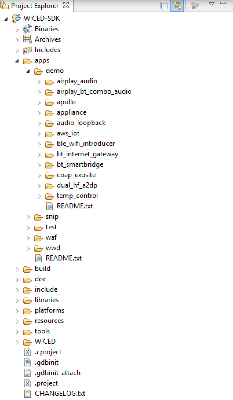
What I can talk about is the first part.  So, I thought that I would show you one of the things that we did with WICED.  First of all, WICED (Wireless Internet Connectivity for Embedded Devices) is the brand name that Cypress uses to describe all of the WiFi, Zigbee and Bluetooth chips and modules that were acquired from Broadcom/Avago.  The other thing we call WICED is the WICED SDK which is used to mean Eclipse plus all of the tools (programer, plugins etc) plus the software library that is used to build products using the WICED chips and modules.

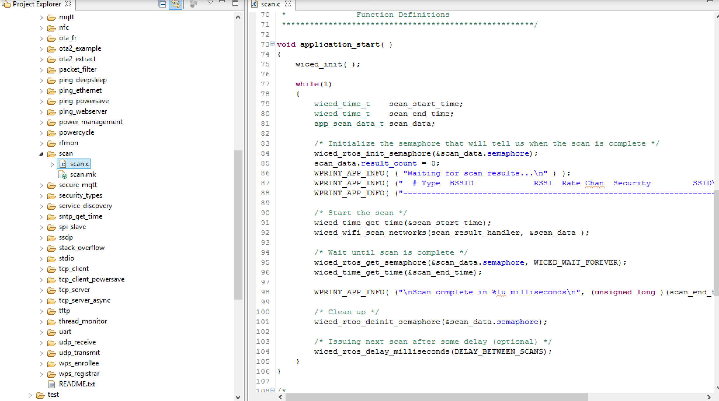
In the world of programming the first example is always “hello world”.  In the world of MCUs the first example is always “blinking led”.  It turns out that the first example in WiFi is “scan” to show that you can see all of the WiFi networks around you.   The purpose of all of these examples is to prove that all of the tools can do their thing.

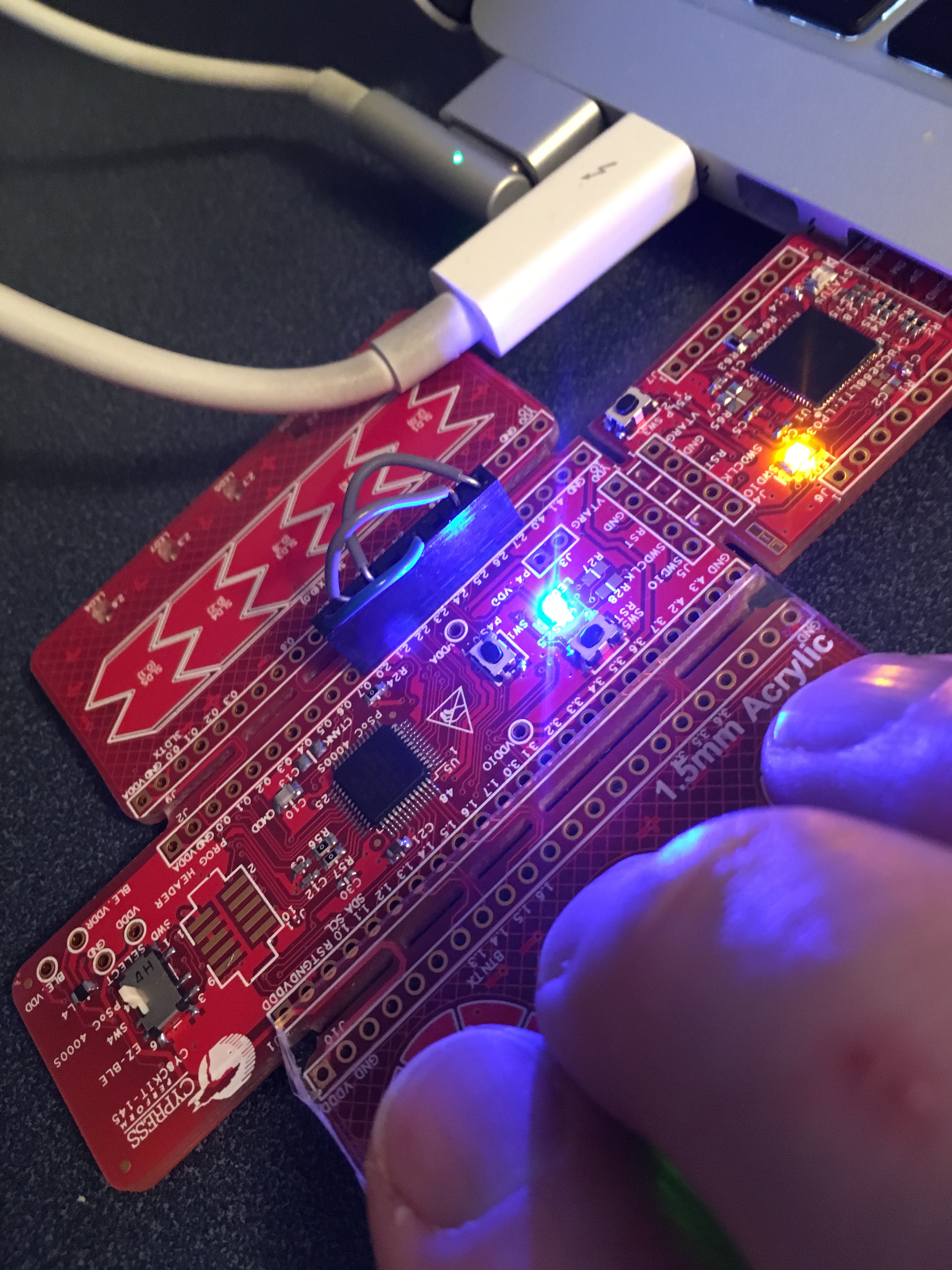
To start with they gave me this devkit, the BCM94343WWCD1_1  IMG_3049

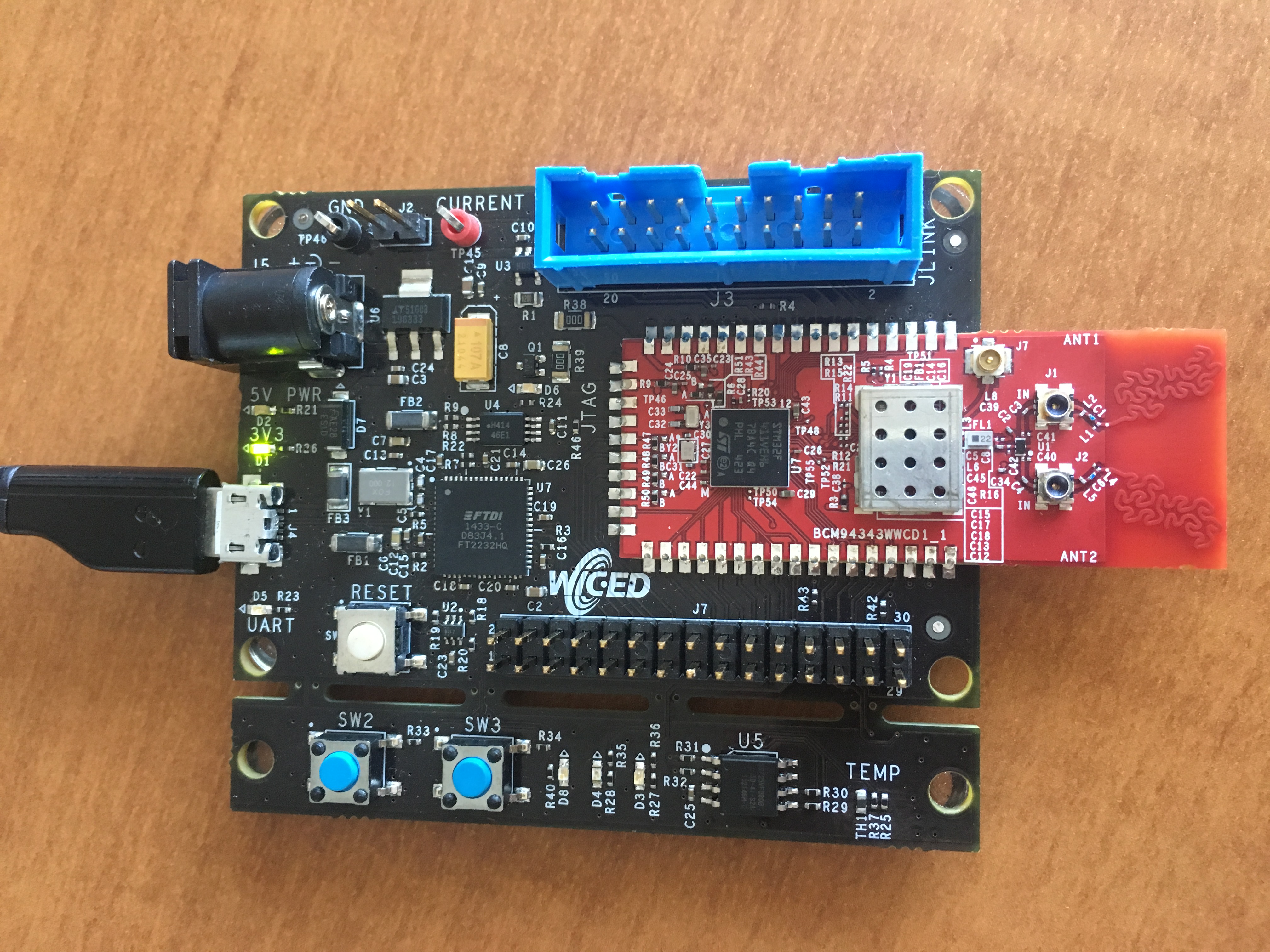
The first thing to do is install WICED 3.7.  When you start WICED you will see a screen like this:

Screen Shot 2016-08-22 at 8.22.06 AM

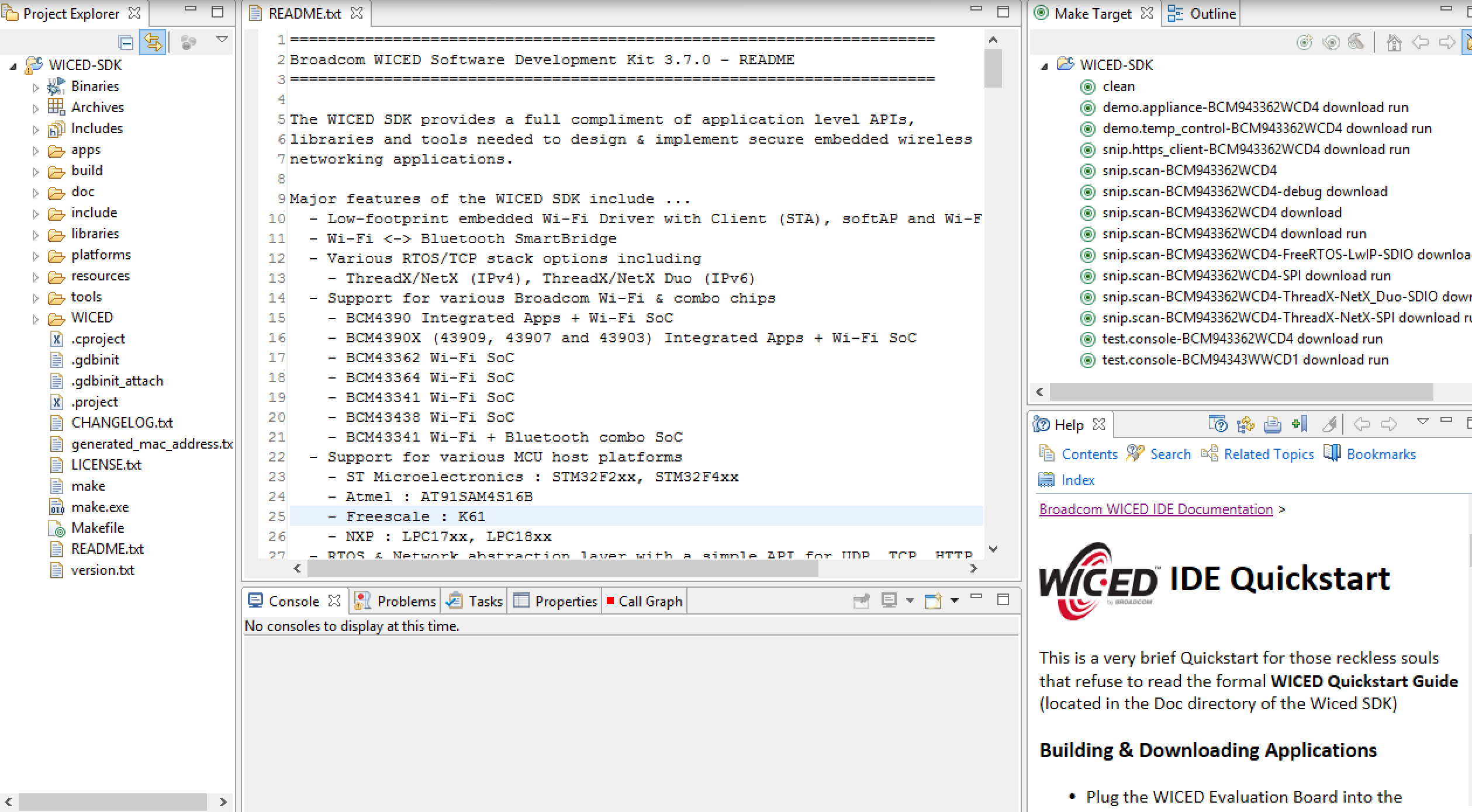
For the purposes of the first design there are two important things to see on this screen.  First on the left side is the project explorer.  It has all of the guts of WICED.  As part of the installation we provide you a bunch of “apps”.  These apps range from simple examples (in the snip folder) to full fledged production quality applications (in the demo folder)

  • demo – full fledged applications
  • snip – short example projects
  • test – tools for debugging and testing wifi
  • waf – WICED Application Framework support (like an OTA Bootloader)
  • wwd – low level driver examples

Screen Shot 2016-08-22 at 8.27.04 AM

The example that I want to build is “scan”  specifically “scan.c”.  That can be found in the apps/snip/scan folder.  In this screenshot you can see that I opened “scan.c”

Screen Shot 2016-08-22 at 8.43.49 AM

The next thing that you need to do is build a “make target”.  The WICED team built a makefile that can seemingly do everything.  The makefile uses the name of the make target to setup all of the options required to do the make.  If you look on the right side of the screen you can see the currently existing targets:

Screen Shot 2016-08-22 at 8.24.40 AM

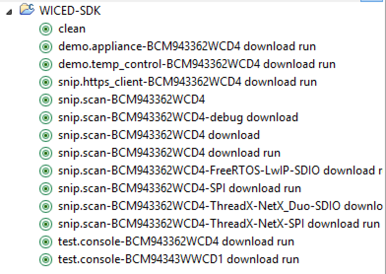
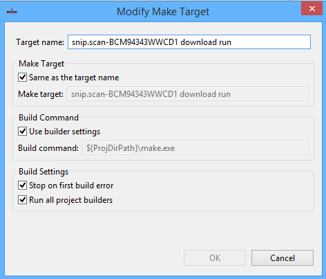
The easiest way to make a new target is to copy/paste a currently existing target.  Then you can right click on the new target and edit it to get things setup correctly.  The target name defines:

  • snip – the directory
  • scan – the subdirectory will the files (scan.c and scan.mk)
  • BCM94343WWCD1 – the name of the devkit (you can see it on the picture of the devkit)
  • download run – instructions to go ahead a boatload and start the app running

Screen Shot 2016-08-22 at 11.32.06 AM

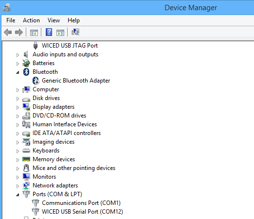
Next, I plug in the devkit.  When it attachs, the devkit will enumerate as two USB devices

  • WICED USB JTAG Port
  • A serial port (in this case on COM12)

Screen Shot 2016-08-22 at 11.29.45 AM

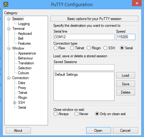
After I plug in the kit I run Putty and attach to COM12 at 115200 baud

Screen Shot 2016-08-22 at 11.36.32 AM

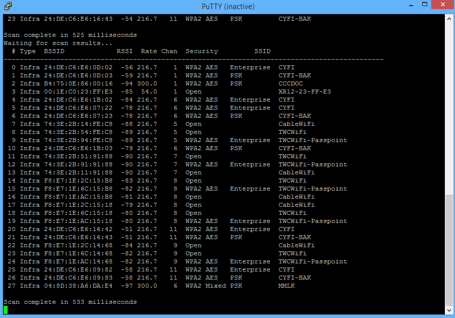
And finally, double click the make target to build, download and run.  After it starts, the Putty screen fills up with all of the WiFI networks that are around me.

Screen Shot 2016-08-22 at 11.30.39 AM

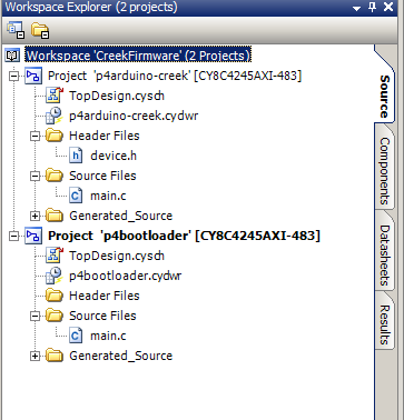
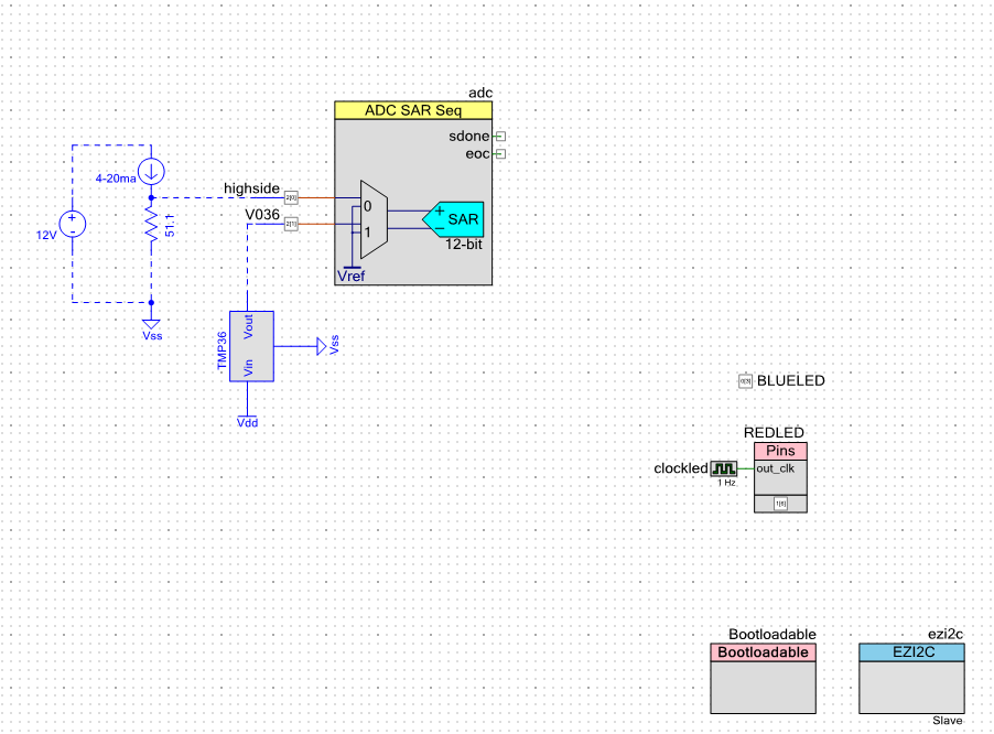
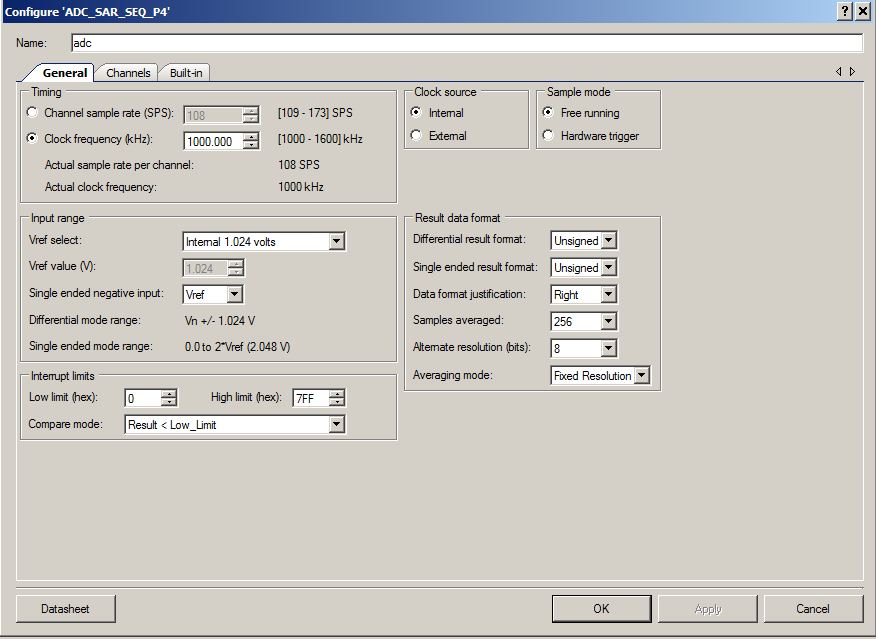
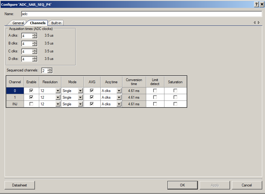
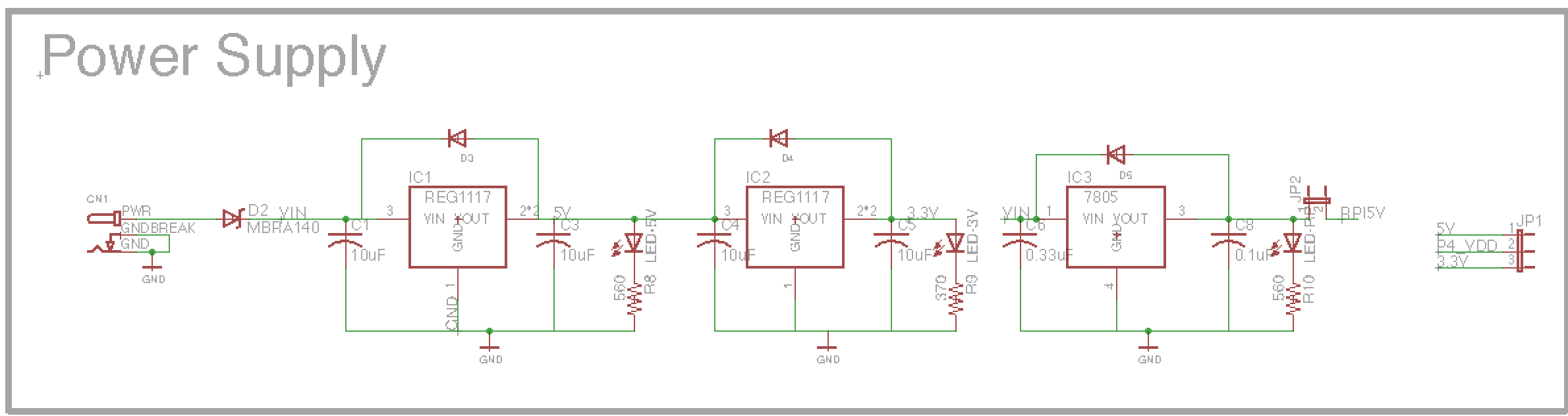
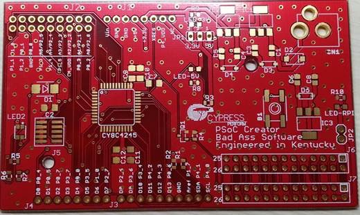
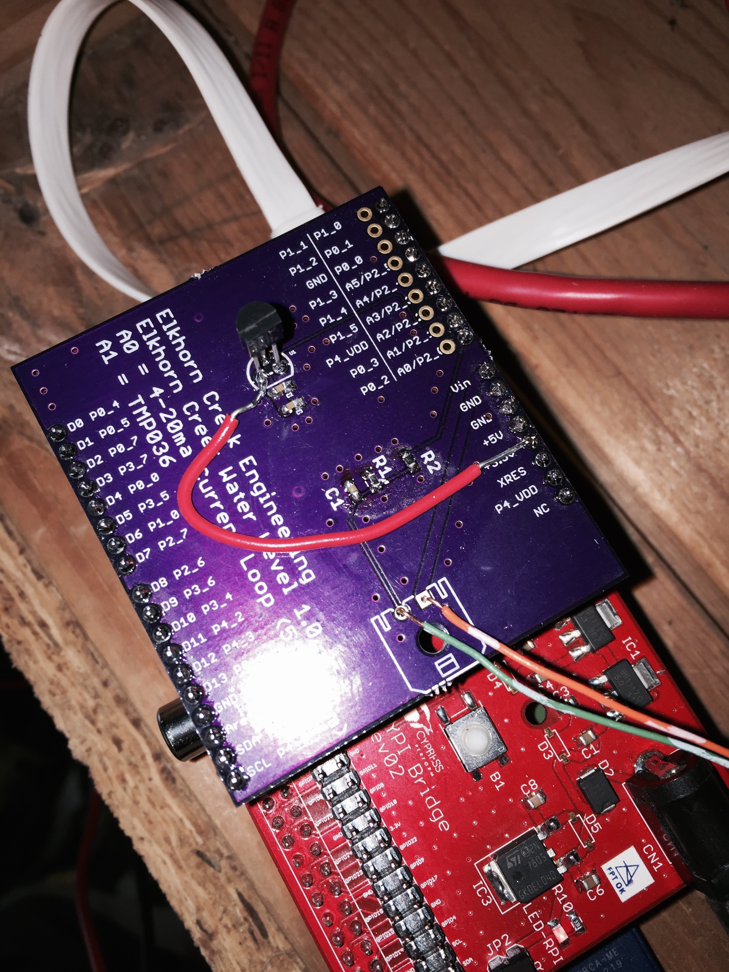
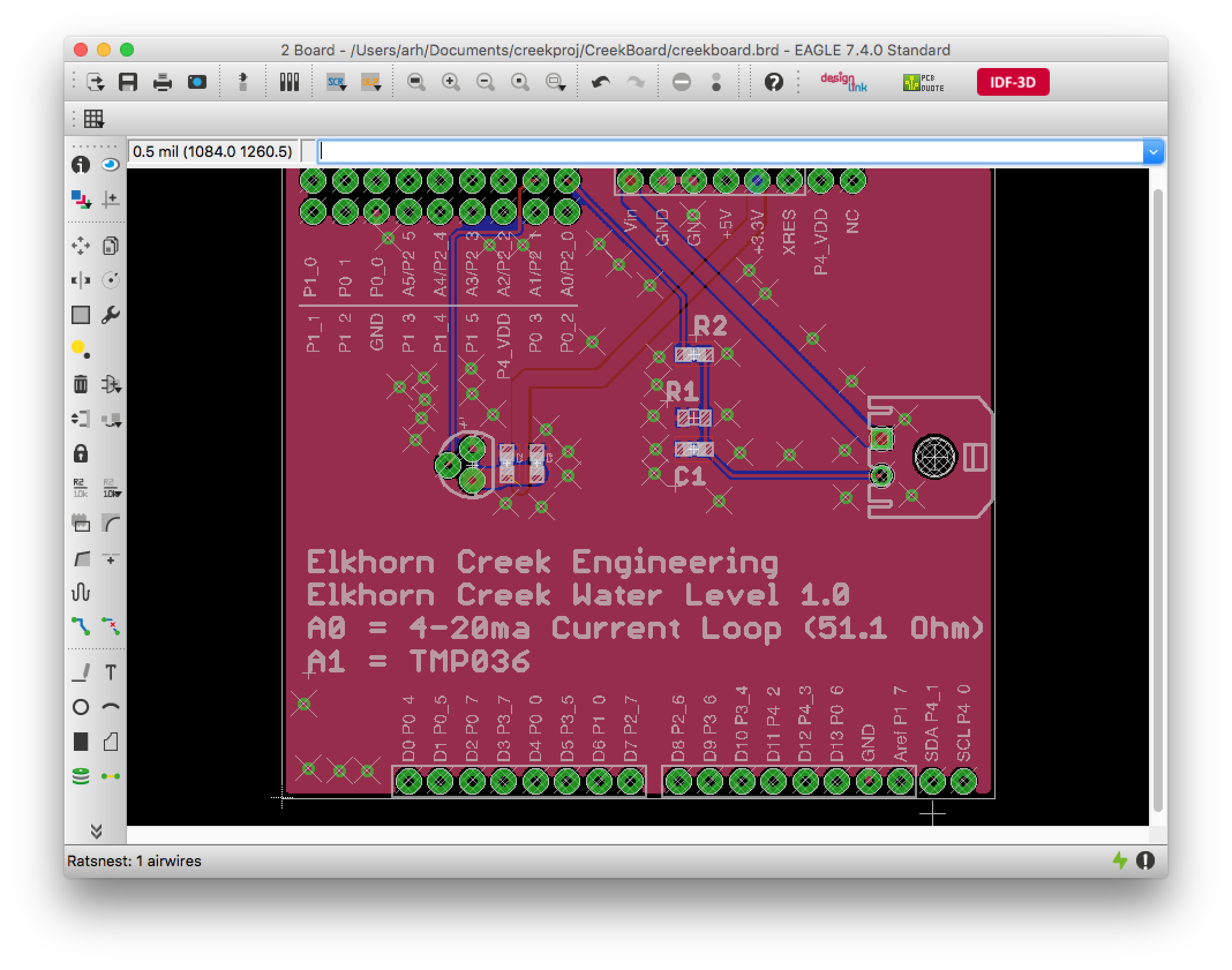
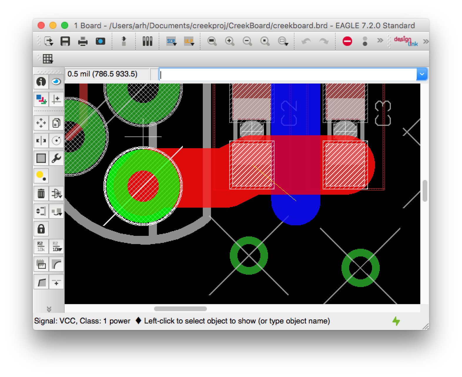
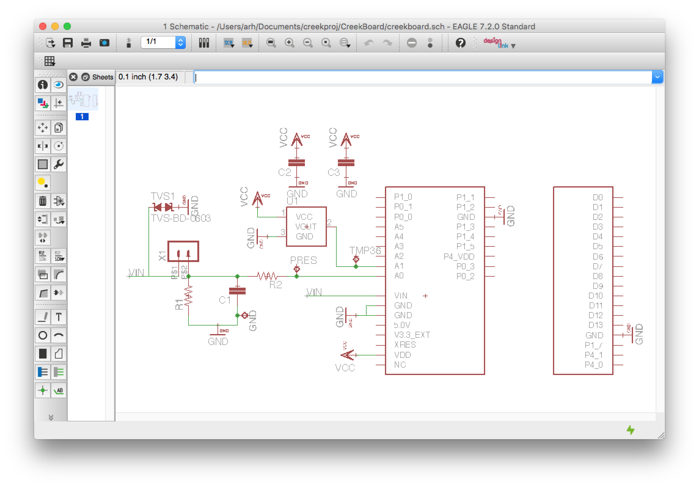
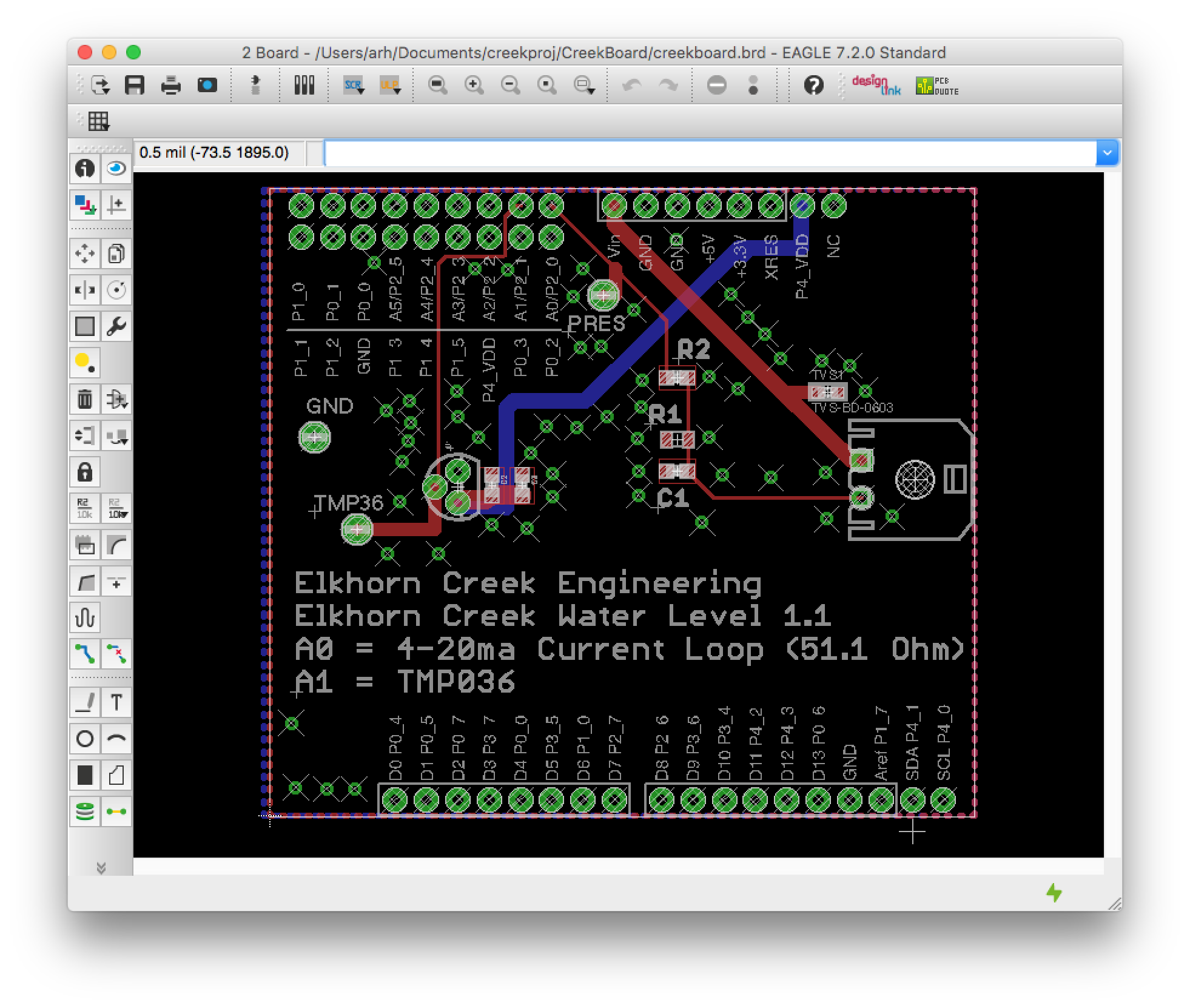
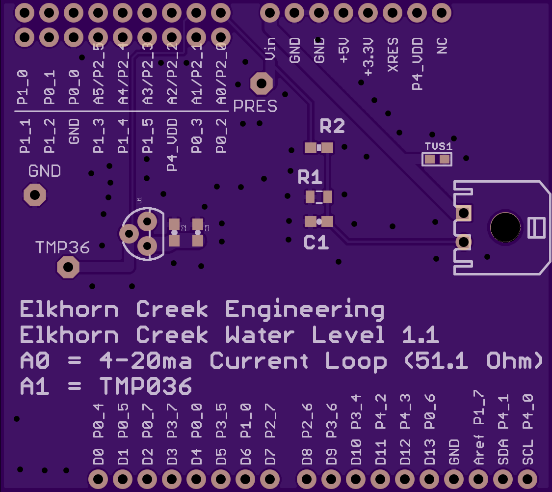
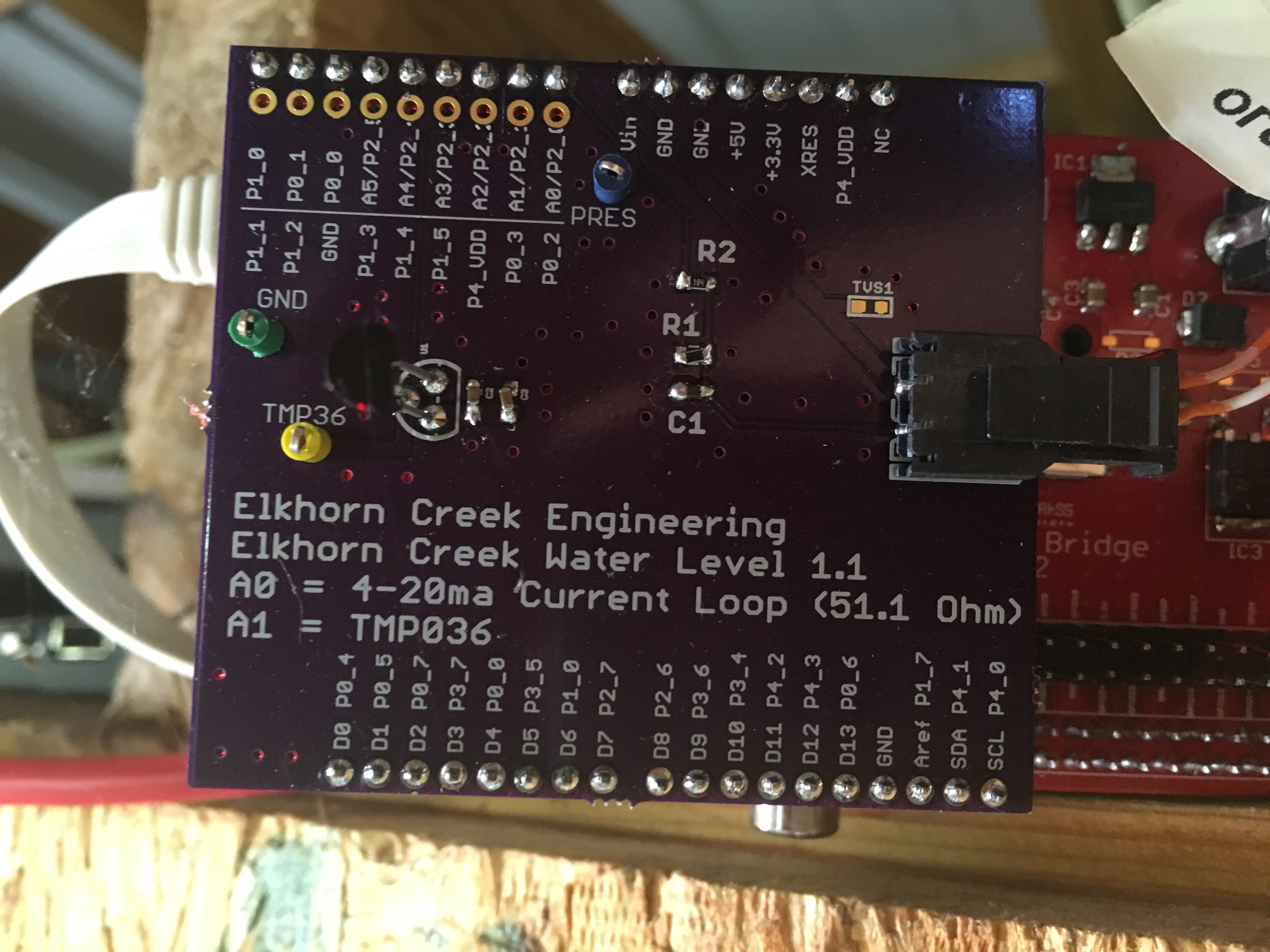
All of that was pretty easy to get going.  Next lets see if I can actually do something.  Last week I showed the guys the Elkhorn Creek Water Level monitoring project and I told them that by the end of this week I would put one of their devkits into that system, so the next several posts will be about that process. (I hope)

The Creek: Testing the Bootloader

In the previous posts I described the main application firmware and the bootloader firmware.  In this post I will take you through the process of verifying that it all works.  In order to do this I need to:

  1. Test the bootloader (verify that I can bootload)
  2. Test the main application firmware (the subject of the next post)
    • Verify the pressure sensor
    • Verify the temperature sensor
    • Verify the I2C communication

Testing Bootloader

Cypress makes a cool programming tool called the MiniProg-3 which we also call CY8CKIT-002.  The MP3 is a multi purpose tool that can be use to:

  • Program and debug Cypress PSoC chips
  • Bridge USB <-> I2C (which I will use to test the firmware)
  • Bridge USB <-> JTAG
  • Bridge USB <-> ISSP

First, I will program the bootloader firmware using PSoC Creator connected via USB to a MP3.  In the photograph below you can see:

  • Mini Prog 3
  • The CYPI Bridge Board with the PSoC 4
  • The 10-pin ARM programming header (which is attached to the grey cable from the MP3)
  • The blue blinking LED.  (after I programmed the board the LED started blinking.  In this picture I caught it on)

Programming the bootloader

At this point it appears that the bootloader is programmed into PSoC4 as the LED is blinking.  In this case I only programmed the bootloader, so there is no application firmware to jump to, so the chip will just keep running the bootloader until the power goes off.

Next, I need to attach another MP3 acting in the role of a USB <–> I2C bridge.  The MP3 will emulate the Raspberry Pi which will be used in the production system, but for now it is easier to test without the added complexity of the RPi.  I am using one MP3 just as a power source for the CYPI board (I could have just plugged in a wall wart).  You can see that I have two wires, one for SDA and one for SCL connected to the correct RPi/CYPI pin.  The other side of the wires are sticking into the correct female connectors on the header of the MP3 (right next to each other at the bottom).

IMG_2728

Then I start the bootloader host which is a program that can read CYACD files (which is just a format of a hex file) and send it out over I2C (or UART) using the bootloading protocol.  First, I select the correct CYACD file from the directory where PSoC Creator put it.  Then I click the download button.

BootloaderHost-a

A few seconds after the boot loading is finished, the blinking blue led turns off and a blinking red led starts.  This indicates that the main application firmware is running.  To verify that the bootloader still works I press the reset switch on the board and the blue led starts blinking for 10 seconds before jumping back into the application firmware.  Good.  The bootloader and application firmware work together correctly.

In the next post I will show you how to use the Bridge Control Panel to verify that the firmware is working correctly.

Index Description
The Creek: IOT for the Elkhorn Creek Introduction
The Creek: Solution Architecture 1.0 Overall architecture
The Creek: Creek Board 1.1 Eagle layout of the board
The Creek: Creek Board 1.0 – RCCA A discussion of the errors in the 1.0 board
The Creek: CYPI, a Raspberry Pi to Arduino Bridge PSoC4 <--> Raspberry Pi Bridge Board
The Creek: PSoC4 Creator Schematic and Firmware Firmware to interface with the temperature and pressure sensors
The Creek: Testing the Firmware Using tools to verify that the PSoC 4 Firmware is working correctly
The Creek: Testing the Bootloader Make sure that you can load new firmware into the PSoC
The Creek: Software Architecture All of the Raspberry Pi software connections
The Creek: Install MySql Instruction to configure MySql
The Creek: Install Tomcat Instruction to configure Tomcat JSP Server
The Creek: Data Collection Java (Part 1) The Java program that reads the I2C and saves it in the database
The Creek: Data Collection Java (Part 2) The Java program that reads the I2C and saves it in the database
The Creek: Create the Chart with JFreeChart Using open source Java charting software to create plots of the Creek Depth
The Creek: Flood Event Data Processor A batch program to create analyze the database and create a table of flood events
The Creek: Flood Event Web Page A batch program to create the flood event web page
The Creek: Creek Server 1.1 Updates to all of the back off server programs to integrate charts
The Creek: JSP Web Page for www.elkhorn-creek.org The JSP program to make the table and display the website
The Creek: Raspberry Pi Clock Stretching Sorting out a bug in the system having to do with the Broadcomm Raspberry Pi Master not functioning well with clock stretching
The Creek: Creek Server 1.2 Caching the web pages to make them faster

The Creek: Testing the Firmware

In the previous post I discussed the process that I used to test the bootloader firmware.  In this post I will walk you through testing the actual application firmware.  As I started working on this post I decided to remind myself of the format of the EZI2C buffer.  Here it is:

DataPacketFormat

The first thing that I immediately noticed was that I did something really dumb.  Specifically I named one of the fields “float pressure” when it is really “float inches”. Oh well.  The DataPacket structure is composed of 4 variables, two of them are 2-byte unsigned integers and two of them are 4-byte float.  As this PSoC is an ARM chip, all of the variables are stored in little endian format-meaning that the Most Significant Byte (MSB) is last.

To help test the firmware, I will use a program called the Bridge Control Panel (BCP).  The BCP is delivered as part of the PSoC Creator installation and is available under the Start->All Programs->Cypress menu.  The BCP can talk to a Miniprog 3 (or any of the Cypress programmers) via the USB port and then bridge to the I2C bus.  It can then act as an I2C master- in my case it will be emulating the Raspberry Pi I2C Master.

After starting the BCP, I first configure the “chart->variable settings”.  This allows me to setup names and sizes of the EZI2C registers that I want to read from the PSoC.  You can see that I added one variable to correspond to each variable in the DataPacket structure.  In the BCP, an “int” is the same as an ARM int16 aka a two byte integer.  I also select “sign” to indicate that the tempCenti is int16 (not uint16).

bcpVariableSetup

After setting up the variables, I first make sure that the BCP is talking to the PSoC4 by pressing “list” button on the BCP.  When I click that button, the BCP tries to read from all of the 127 valid I2C addresses.  If it gets an “ACK”, then it reports that it can talk to that device.  On the screen below you can see that it sees “address: 10 08” which is the I2C address of my PSoC4.

The next step is to tell the BCP how to read the EZI2C registers.  First I write a 0 to address 8 with the “w 8 0;” command.  This sets the “data pointer” t0 0, meaning the start of the register space.  I then issue command to read 12 bytes, each byte has a name that corresponds to a byte in the “variables” configured in the previous step.  An example is “@0presscount” which corresponds to the least significant byte of the presscount variable and “@1presscount” which corresponds to the most significant byte of the presscount variable.

After setting up the variables, I press “return” to issue the command.  The BCP returns “r 08+ 00+ 00+ AC+ 08+ 8A+ E4+ D0+ C2+ 9A+ 99+ B1+ 41+”.  What does that mean? The R means that it did a read.  The 08+ is the address of the I2C and the + means and “ACK”.  Each of the other bytes+ are the other 12 bytes read in the command.  I use this website to covert the 4-byte hex float(s) to decimal and I get:

  • pressCount = 0x0000 : There is 0 volts attached to the input which is true
  • tempCenti = 0x08AC = 2200 (that makes sense 22.2 degrees c * 100 ~= 2200)
  • pressure = 0xC2D0E48A = -104.44636535644531 … that makes sense rememberdp.pressure = (((float)dp.pressureCounts)-408)/3.906311:
  • temp = 0x41b1999A = 22.200000762939453 c = 71.9f [ok that makes sense]

bcpMainScreen

The next step is to attach a bench power supply to the pressure input (I bought this one from eBay).  I will use the variable voltage to simulate different pressures.  Recall from the schematic that the pressure sensor acts as a current source that is then driven into a 51.1 ohm resistor.  Here is the schematic:

pressureSchematic

With this setup if I put in 0.51V on the “high side” I should get [V=IR] 0.51V = I * 51.1Ohm so I= 0.01 A.  You can see from the picture that is what I get (or pretty damn close).  When I press return on the bridge control panel (see it in the screen shot above) I get “r 08+ E4+ 03+ C0+ 08+ 91+ 86+ 16+ 43+ 33+ 33+ B3+ 41+” which means

  • pressCount = 0x03E4 = 996 counts.  The range of the ADC is 4096 counts (in single ended mode)  and 0 –> 2.048V so 996 counts is 0.498v
  • tempCenti = 0x08C0 = 2200 (that makes sense 22.2 degrees c * 100 ~= 2200)
  • pressure = 0x43168691 =  150.52565002441406 [that works… remember the equation]dp.pressure = (((float)dp.pressureCounts)-408)/3.906311
  • temp = 0x41B33333 = 22.399999618530273 c = 72.3f [ok that makes sense]

pressure-05volt

For the last test of the pressure sensor input I put the variable supply to 1.0V which makes 0.019 mA.  Once again V=IR 1V/51.1Ohm = 0.0196 A.  Ok Ohms law still works.  Then I press return and I get “r 08+ 98+ 07+ C0+ 08+ DD+ 9A+ C4+ 43+ 33+ 33+ B3+ 41+ p”.  When I decode that I get

  • pressCount = 0x0798 = 1944 counts.  The range of the ADC is 4096 counts (in single ended mode)  and 0 –> 2.048V so 1944 counts is 0.972v (that is pretty damn close)
  • tempCenti = 0x08C0 = 2240 (that makes sense 22.4 degrees c * 100 ~= 2240)
  • pressure = 0x43C49ADD = 393.2098693847656 [that works… remember the equation]dp.pressure = (((float)dp.pressureCounts)-408)/3.906311:
  • temp = 0x41B33333 = 22.399999618530273 c = 72.3f [ok that makes sense]

Pressure1v

In the next test I will go into graphing mode and use the “repeat” button to run I2C reads as fast as possible.  I will then sweep the voltage on the bench power supply and plot the pressure and the counts to make sure that makes sense.  It looks good, here is the plot:

bcpGraphofPressure

In the next test I use a Fluke Thermocouple to verify that the TMP036 is reading the correct temperature.  You can see that when I put the thermocouple right on the sensor it reads 23.4 degrees C.  I then turned the camera towards the screen and took a picture of the plot.  In that plot you can see the temperature bouncing around 22.5.  The bounce is  +- 1 count (literally noise) of the ADC .  I am not sure what the cause of the 0.9 degree difference between the Fluke and the TMP036, it could be several things including the accuracy of the TMP036, the accuracy of the Fluke, the accuracy of the PSoC4 ADC, where I am measuring, etc.  But less than a degree really doesn’t matter to me.

temp-fluke

temp-bcp

In the last test I make a graph of the temperature while I am grabbing the TMP036 which causes the temperature to rise.  After a bit of time I let go of the sensor and you can see the temperature fall.

bcpGraphOfTemperature

At this point it looks like the bootloader is working and that the PSoC 4 firmware is working.  In the next post I will talk about the overall server software architecture.

Index Description
The Creek: IOT for the Elkhorn Creek Introduction
The Creek: Solution Architecture 1.0 Overall architecture
The Creek: Creek Board 1.1 Eagle layout of the board
The Creek: Creek Board 1.0 – RCCA A discussion of the errors in the 1.0 board
The Creek: CYPI, a Raspberry Pi to Arduino Bridge PSoC4 <--> Raspberry Pi Bridge Board
The Creek: PSoC4 Creator Schematic and Firmware Firmware to interface with the temperature and pressure sensors
The Creek: Testing the Firmware Using tools to verify that the PSoC 4 Firmware is working correctly
The Creek: Testing the Bootloader Make sure that you can load new firmware into the PSoC
The Creek: Software Architecture All of the Raspberry Pi software connections
The Creek: Install MySql Instruction to configure MySql
The Creek: Install Tomcat Instruction to configure Tomcat JSP Server
The Creek: Data Collection Java (Part 1) The Java program that reads the I2C and saves it in the database
The Creek: Data Collection Java (Part 2) The Java program that reads the I2C and saves it in the database
The Creek: Create the Chart with JFreeChart Using open source Java charting software to create plots of the Creek Depth
The Creek: Flood Event Data Processor A batch program to create analyze the database and create a table of flood events
The Creek: Flood Event Web Page A batch program to create the flood event web page
The Creek: Creek Server 1.1 Updates to all of the back off server programs to integrate charts
The Creek: JSP Web Page for www.elkhorn-creek.org The JSP program to make the table and display the website
The Creek: Raspberry Pi Clock Stretching Sorting out a bug in the system having to do with the Broadcomm Raspberry Pi Master not functioning well with clock stretching
The Creek: Creek Server 1.2 Caching the web pages to make them faster

The Creek: PSoC 4 Bootloader Schematic + Firmware

A bootloader is a firmware program that can update the application firmware in an embedded system without using a programmer (like the Miniprog-3).  This is a convienient way to fix bugs, release features, etc. without having to be physically at the system.  As a developer you can update your design, then create a “hex” file image, then release that image (through email, the internet, etc) to be installed on all of your remote devices.  Once your new hex file arrives at the host computer, the bootloader has the job of flashing the new firmware into your system.  You can read more detail about bootloading in the excellent Cypress application note AN86526 PSoC4 I2C Bootloader.

In general, bootloaders are triggered by some external event (like a chip reset, a trigger from a GPIO, or a command from the application firmware).  The bootloader then listens for communication from a host computer.  The host computer could be lots of different things including a cell phone, a central application processor, or an external computer plugged into your system.  Once the bootloader starts:

  • If there is no communication it will generally timeout after a set time, then jump into the application firmware to put the system into normal application mode.
  • If there is communication, it will copy a new application from the host computer and then write it into the flash in the correct place.  There is a special case called a “dual application” boot loader.  This provides safety by keeping and old image still in flash in case there is a problem bootloading the new firmware.

Here is a picture of the architecture:

bootloading

In the Cypress language the bootloadable is an application image that can be bootloaded by the bootloader.

When I am making firmware like this I generally put two projects in the same workspace.  One project is the bootloader and the other project is the bootloadable. This is exactly what you will find in in the PSoC Creator workspace called CreekFirmware on github.  The first project is called p4arduino-creek which is the main application firmware that  I discussed in detail in the previous post.

This bootloader, called p4bootloader, is a simple I2C bootloader.  After the chip resets it:

  • Starts blinking the blue led to indicate that it is in bootloader mode
  • Waits 10 seconds to hear I2C communication
  • If there is none then it jumps into the main application (called the bootloadable)
  • It there is then it starts the boot loading process

The schematic is simply:

  • An I2C Slave
  • A bootloader component
  • A blinking LED (a clock tied directly to an output pin)

BootloaderSchematic

When you configure the bootloader component you need to select which communication interface to use.  In this case it is the “I2C”.  Then you configure how long you want to wait before timing out and jumping into the main application.  In this case 10000ms a.k.a. 10s

BootloaderConfiguration

The last step is to start the bootloader component in the firmware.

BootloadingFirmware

That is it.  In the next post I will discuss the steps I took to test the firmware.

Index Description
The Creek: IOT for the Elkhorn Creek Introduction
The Creek: Solution Architecture 1.0 Overall architecture
The Creek: Creek Board 1.1 Eagle layout of the board
The Creek: Creek Board 1.0 – RCCA A discussion of the errors in the 1.0 board
The Creek: CYPI, a Raspberry Pi to Arduino Bridge PSoC4 <--> Raspberry Pi Bridge Board
The Creek: PSoC4 Creator Schematic and Firmware Firmware to interface with the temperature and pressure sensors
The Creek: Testing the Firmware Using tools to verify that the PSoC 4 Firmware is working correctly
The Creek: Testing the Bootloader Make sure that you can load new firmware into the PSoC
The Creek: Software Architecture All of the Raspberry Pi software connections
The Creek: Install MySql Instruction to configure MySql
The Creek: Install Tomcat Instruction to configure Tomcat JSP Server
The Creek: Data Collection Java (Part 1) The Java program that reads the I2C and saves it in the database
The Creek: Data Collection Java (Part 2) The Java program that reads the I2C and saves it in the database
The Creek: Create the Chart with JFreeChart Using open source Java charting software to create plots of the Creek Depth
The Creek: Flood Event Data Processor A batch program to create analyze the database and create a table of flood events
The Creek: Flood Event Web Page A batch program to create the flood event web page
The Creek: Creek Server 1.1 Updates to all of the back off server programs to integrate charts
The Creek: JSP Web Page for www.elkhorn-creek.org The JSP program to make the table and display the website
The Creek: Raspberry Pi Clock Stretching Sorting out a bug in the system having to do with the Broadcomm Raspberry Pi Master not functioning well with clock stretching
The Creek: Creek Server 1.2 Caching the web pages to make them faster


The Creek: PSoC 4 Creator Schematic + Firmware

In this post I will describe the PSoC Creator schematic and firmware that I built to run the PSoC4.  You can find the project on github.  After you open the project in PSoC Creator you will find two projects in the workspace explorer:

  1. p4ardino-creek: This project starts running 10 seconds after the chip powers up.  It uses PSoC Analog to Digital Convertor to read the pressure sensor and the temperature sensor.  It then convert the data to a readable form and stores it into the EZI2C buffer to be read by the Raspberry PI.
  2. p4bootloader: This project runs for 10 seconds when the chip is rebooted.  If it detects the Raspberry Pi host trying to load new firmware it will “bootload”.  If after 10 seconds it doesn’t hear anything, it will run the p4arduino-creek application.  I will describe how the bootloader works in the next post.

CreekWorkspace

p4ardunio-creek

The schematic for this project contains four sections

  1. The Analog to Digital convertor and the “external” schematic of the pressure current loop.  The elements in blue are external to the PSoC and are there just for documentation.
  2. The Red and Blue LED pins and the clock that drives the Red LED to blink
  3. The EZI2C which serves as the I2C Slave for the Raspberry Pi to read
  4. The Bootloadable component which allows this project to be boot loaded.

The configuration of each of elements is show below.

Creek Schematic

The ADC is configured to run as slowly as possible (1000 SPS).  I have also enabled the averaging which automatically averages 256 samples.  This effectively makes a low pass filter to remove noise.  This is possible because the pressure and temperature move very slowly as compared to the speed at which they are sampled.  The SAR ADC in the PSoC is inherently differential, I tell the ADC that I want the negative channel to be connected to a stable VREF.  This allows me to measure between 0V and 2*vref = 2.048 volts.

ADC Configuration 1

On the ADC channels TAB I enable two channels, both single ended, both with averaging turned on.  Channel 0 is connected to the pressure sensor (on Arduino pin A0 = PSoC Pin P2[0]) and channel 1 is connected to the TMP036 (on Arduino pin A1 = PSoC Pin P2[1])

ADC Configuration Screen 2

For this design I setup the PSoC4 to act as an EZI2C slave.  EZI2C means that the chip follows the EEPROM protocol which many many I2C masters understand.  The only thing that I configure in this case is to use the slave address of 0X08.

CreekEzI2C

For this project to be compatible with a bootloader it needs the bootloadble component instantiated.  In this case I use all of the default configurations.  When I make changes to the firmware in the future I will up-rev the version numbers.  These settings are here to prevent you from accidentally overwriting and newer rev of the firmware or putting in the wrong application type.

CreekBootLoadableConfig

In order for the bootloadable to work I need to tell it where its  “bootloader” image resides.  Remember from above that I put both projects in the same workspace.  So, what I need to do is browse through the directory hierarchy into the bootloader project and selects its ELF and HEX files.  If you want to read more about PSoC4 Bootloading you can read AN86526 entitled “PSoC 4 I2C Bootloader”

BootloableDependencies

One of the unique features of a PSoC is its ability to do hardware based design.  In this design I want a slowly blinking LED to indicate that the system is running.  For this task I have to configure the pin to let one of the internal clocks drive it.  To make this work you need to selected the output mode as “Clock”.

redLedPin

And you need to selected the “Out clock” as external.

redLedClock

Now, I want to turn off the Blue LED.  As the LED is active Low, to turn it off you write a 1 to the pin.  I do this as part of the setup of the pin by setting the initial drive state to high.

blueLED

The last step in the device configuration is to select the proper pins on the Design Wide Resources (DWR) pins tab.  Not setting the pins correctly is one of the most frequent errors that users make with PSoC Creator.

creekFirmwarePins

The firmware for the project is simple.  In the first section (lines 3-8) I define a packed structure to serve as the I2C buffer.  The __attribute__((packed)) tells the compiler to put all of the members of the structure in contiguous bytes.  In the structure I defined below, if I had not marked it is packed, it is likely that the compiler would have put two bytes of padding after the pressureCounts and two bytes after the centiTemp.  It would have done this to work align those datatypes to make the memory access more efficient.

The next section (lines 17-23) I initialize the system and start the components.

The the main body of the program (lines 27-43) I ask the ADC if it is done reading the voltages,  if not go on, if so then calculate the different values and store them in the I2C buffer.  The “CyEnterCriticalSection” prevents an I2C interrupt from reading the buffer before the data is completely written to prevent a partial read of the data.

CreekFirmwareMainC

In the next post I will explain boot loading and the p4bootloader project.

Index Description
The Creek: IOT for the Elkhorn Creek Introduction
The Creek: Solution Architecture 1.0 Overall architecture
The Creek: Creek Board 1.1 Eagle layout of the board
The Creek: Creek Board 1.0 – RCCA A discussion of the errors in the 1.0 board
The Creek: CYPI, a Raspberry Pi to Arduino Bridge PSoC4 <--> Raspberry Pi Bridge Board
The Creek: PSoC4 Creator Schematic and Firmware Firmware to interface with the temperature and pressure sensors
The Creek: Testing the Firmware Using tools to verify that the PSoC 4 Firmware is working correctly
The Creek: Testing the Bootloader Make sure that you can load new firmware into the PSoC
The Creek: Software Architecture All of the Raspberry Pi software connections
The Creek: Install MySql Instruction to configure MySql
The Creek: Install Tomcat Instruction to configure Tomcat JSP Server
The Creek: Data Collection Java (Part 1) The Java program that reads the I2C and saves it in the database
The Creek: Data Collection Java (Part 2) The Java program that reads the I2C and saves it in the database
The Creek: Create the Chart with JFreeChart Using open source Java charting software to create plots of the Creek Depth
The Creek: Flood Event Data Processor A batch program to create analyze the database and create a table of flood events
The Creek: Flood Event Web Page A batch program to create the flood event web page
The Creek: Creek Server 1.1 Updates to all of the back off server programs to integrate charts
The Creek: JSP Web Page for www.elkhorn-creek.org The JSP program to make the table and display the website
The Creek: Raspberry Pi Clock Stretching Sorting out a bug in the system having to do with the Broadcomm Raspberry Pi Master not functioning well with clock stretching
The Creek: Creek Server 1.2 Caching the web pages to make them faster


PSoC4000s & The SmartIO – Part 3

For this post, I wanted to build a simple state machine inside of the SmartIO.  So I decided to build a 3-bit counter.  On the CY8CKIT145 board, port 2 is mostly connected to LEDs.  When you look at the picture below you can see that the LEDs on the left side of the board are easiest to see, so I decided to use them to indicate the state of the counter.  You can see from my notes that I was originally considering using LED9,11,10 which are the three LEDs on the CapSense buttons board.  I also considered using LED5,6,8 which are on the right side of the slider board, but I ruled all of that out because they were hard to see.

IMG_2737

To build this project you start by creating the schematic.  In this case I copied the design from the previous post called “145MutualCap” which had 3 CapSense buttons and 3 LEDs (LED10,11,9).  I then added:

  • A 5 KHz Clock to drive the PWM
  • A PWM to divide down the clock to a speed that I could see and provide a clock for the counter
  • A Smart IO
  • 4 Output Pins to drive LEDs (P27, P26, P25, P23)

counter-schematic-1

Next I configured the PWM with a 50% duty cycle and a Period of 10000.  This results in a 0.5Hz clock:

smartiopwm

Then I configure the SmartIO.

  • Setup “data4” as an input to the Smart IO.  Data 4 is the line out 0 of the TCPWM0
  • Setup “data5” as an input to the Smart IO.  Then configure it to be the “clock” for the smart IO. Data 5 is the Line_N of TCPWM0.  Originally I wanted to be able to have the clock drive LED5 as well, but this can create a timing hazard in the Smart IO and is not allowed (which is why I mirror data 4 onto the output P25.
  • Setup GPIO 7,6,5, and 3 as outputs (these outputs are connected to P27, P26, P23 which are the LEDs on the slider board.  GPIO5 is connected to P25 that is the user LED on the main board

smartioconfig

Then I configure LUTs 6, 3, 7 to implement the state table of a counter

state

lut6

lut3

lut7

I want to be able to see the clock (the PWM input data4) ticking so I create a transparent LUT (000 = 0 and 111 = 1) for LUT5 which is attached to P25 which is the LED on the main board.

lut5

After this is done I need to assign the Pins.

smartiopinassignment

Followed by the very simple firmware which is copied from the previous design.  The only new code is line 9 to turn on the PWM.

main

You can find this PSoC Creator workspace on github in the directory called “SmartIO”.  This project is called “SmartIOCountUp”.

Index Description
PSoC4000s & The SmartIO – Part 1 An introduction to the SmartIO and first project
PSoC4000s & CSX Mutual CapSense Buttons Part 1 Using mutual capacitance
PSoC4000s & CSX Mutual CapSense Buttons Part 2 Using the CapSense tuner
PSoC4000s & The SmartIO – Part 2 A 3 input XOR logic gate
PSoC4000s & The SmartIO – Part 3 A 3 bit up counter state machine
PSoC4000s & The SmartIO – Part 4 Using an external clock with the Smart IO
PSoC4000s & The SmartIO – Part 5 Triggering an interrupt

PSoC4000s & The SmartIO – Part 2

In the previous posts I introduced you to the Smart IO.  I also went through the instructions to create CapSense Buttons using the new Mutual-cap CSX mode of the PSoC4000S.  In this post I am going to use the three CapSense buttons on the CY8CKIT-145 as inputs to the Smart IO.  I want to create a simple logic function P25 = !XOR(P24,P26,P27).  This will cause the LED that is attached P25 to light up when there is an odd number of 1’s on P24,P26,P27.  The equation is slightly strange because the LED is wired as active low (it lights up when there is a 0 written to it)

To make this work I soldered an 8 pin female header to Port 2 of my development kit.  I then wired:

  • P20 <–> P24
  • P21 <–> P26
  • P22 <–> P27

You can see all of that in the picture below.

IMG_2744

The next step is to create the schematic for this design.  I started from the Mutual Capacitance project that I talked about in the previous post.  It has three LEDs and the Capsense Buttons.  I then add

  • Three digital output pins (P20,P21,P22) to drive the three inputs to the SmartIO
  • Three digital input pins (P24,P26, P27) to use as inputs to the SmartIO
  • One digital output pin (P25) to drive the LED
  • The Smart IO block

3xorschematic

The next step is to configure the SmartIO.  I setup P24,P26,P27 as “inputs” and setup P25 as an “output”

smartio-config

Then I configure the LUT to match the logic equation: P25 = !XOR(P24,P26,P27)

LUT5

Lastly I assign the pins to the correct physical pins on the chip.

dwr

Then I create the firmware by copying the main.c from the earlier CapSense example.  I then add the small amount of code to glue it all together:

  • Line 7: start the SmartIO
  • Lines 27-29: Write to P20,P21,P22 based on the state of the input buttons.

3xormainc

You can find this PSoC Creator workspace on github in the directory called “SmartIO”.  This project is called “3Xor”.

In the next post I will show you how to make a state machine using the Smart IO.

Index Description
PSoC4000s & The SmartIO – Part 1 An introduction to the SmartIO and first project
PSoC4000s & CSX Mutual CapSense Buttons Part 1 Using mutual capacitance
PSoC4000s & CSX Mutual CapSense Buttons Part 2 Using the CapSense tuner
PSoC4000s & The SmartIO – Part 2 A 3 input XOR logic gate
PSoC4000s & The SmartIO – Part 3 A 3 bit up counter state machine
PSoC4000s & The SmartIO – Part 4 Using an external clock with the Smart IO
PSoC4000s & The SmartIO – Part 5 Triggering an interrupt

PSoC4000s & CSX Mutual CapSense Buttons Part 2

In the previous post I gave you the instructions to get the new Mutual Capacitance buttons going on the CY8CKIT-142.  In this post I will talk about how to add the Capsense Tuner to your project.  The Capsense tuner can talk to your design while it is running, then report back to you the parametric of your design.

First you need to add the tuner to your project.  In order to do this, start with the last design, then add an EzI2C component.  Here is the new schematic:

Tuner-Schematic

Then you configure the EZ2IC to have 16 bit sub addresses.

Tuner-EzConfig

Then assign the EZI2C pins to the KitProg I2C bridge pins

Tuner-DWR

The last step is to write the firmware which is almost exactly what you had in the last project except

  • Lines 8-9 which start the capsense block and setup the Capsense memory buffer to be readable by the remote host
  • Line 21: which updates the Capsense memory buffer with the current state of the capsense parameters

tuner-firmware

Once all of this is done, build and program the device.  Then start the capsense tuner by right clicking the Capsense component in the schematic and saying “run Tuner”

launch-tuner

Then configure the tuner communication parameters from the “Tools->Tuner communication setup” menu.  These should match what you have setup in the EZI2C component.  Specifically you need set the I2C addresses to be the same, and you need to have the sub-address set to “2-bytes” which is the same as the 16-bit sub-address which you set in the component above.

tuner-comm-setup

The next step is to press “connect”  and the “start”.  First make sure that your three buttons are working.  In the picture below you can see that I am touching Buttons 1 and 2 as they are “active” (red color) which means that their signal is above the threshold.

2-buttons

The next step is to look at a “graph view” of button 0.  You can do this by pressing “graph view” and selecting Button0_Rx0.  Once I switch to this view I touch the button 9 times.  You can see that as there are 9 button touches in the Status window.  A status of 1 means that the button is active and a status of 0 is an inactive.

In the sensor data window you can see the “baseline” which is the noise on the sensor node without a touch.  The blue line is the “RawCounts” which the amount of signal on the node.

In the middle window you can see the “Sensor Signal” which is the Sensor Data minus the baseline.  Any time the Sensor Signal is above the touch threshold then the sensor status is active.

Tuner-graph

The last step is to use the SNR measurement tab to see how robust your design is.  First click on the “SNR Measurement” tab.  Then pick out which sensor you will measure.  In this case I have setup measurement on “Button_0”.  Then click on “Acquire noise” and wait.  It will make the graph shown below which says that my noise is about 3008-2995 or about 13 counts.

BaselineNoise

The next step is to see how much signal you get.  Start this process by pressing “Acquire Signal” and touching the correct button.  You can see orange line represents the amount of signal when you are touching the sensor.  The system will then calculate the SNR which in this case is 56.85 which is tons.

SNR

The last thing that you could do is change the Capsense parameters in the sensor parameter screen.  For instance you could change the threshold from 100 to a bigger number to give more reliable touches.

Parameters

OK.  Now I have my capsense buttons working.  In the next posts Ill be ready to talk more about the Smart IO.

You can find this PSoC Creator workspace on github in the directory called “145MutualCap”.  This project is called “TunerMutualCapButtons-145”.

PSoC4000s & CSX Mutual CapSense Buttons Part 1

In the previous post I talked about my original goal to learn about the SmartIO.  But, in order fully try out the SmartIO I needed an input source.  On this board I had only one easy input from the factory – specifically the mechanical button on P0[7]- but I wanted to have multiple switches.  Well, the obvious choice was to use the three Capsense Buttons on the user interface expansion board.   When I looked at that board closely I remembered that the buttons were put there to support the new Capsense functionality of the PSoC4000s family.  Inside of Cypress we call the new feature “CSX”, but its real name is “Mutual Capacitance”.  Mutual Capsense works by transmitting a signal on the “Tx” pin and then receiving that signal by capacitively coupling that signal through your finger into the “Rx” line.  Here is a picture of that part of the PCB schematic and a zoom in of the board.  You can see that there are three different size buttons.  Each of the buttons is composed of an even number of pie shaped segments.

mutual-cap-buttonsScreen Shot 2016-03-06 at 2.03.17 PM

The mutual capacitance technique has a much higher Signal-to-Noise Ratio (SnR) as compared to the Self Capacitance technique of previous chips and as a result is more immune to noise and can work through a thicker overlay.  I thought that I would try putting on overlay on my board, so I cut out a piece of 1.5mm acrylic and used double sided tape to attach it to my board.  You can see it in the photograph above.

To make this work I started by creating a new project called “MutualCapButtons”.  I then added the Capsense component and three digital output pins (one for each of the three LEDs on the expansion board).  Here is the schematic:

mutual-button-schematic

The next step was to configure the CapSense block by double clicking it.  I then added three buttons and set the sensing mode to CSX (Mutual-cap).

mtutual-cap-config

It is possible to have dedicated Tx/Rx pins or you can share the Txs.  To do this, select “Advanced” and “Widget details”.  Then select “Button1_Tx”  and choose its sensor to be the same as “Button0_Tx”.  On this design I shared the Tx between all three of the buttons.

Mutual-sharing

The next step is to assign the pins to the correct Port/Pin locations on the chip:

button-pin-assignments

The last step is to write the firmware

  • Lines 8-10 Start the capsense block and get the scanning going
  • Line 14: If the capsense block is done scanning then process the results
  • Line 16: Take all of the raw data from the scan and setup all of the status information
  • Lines 18-20: If the buttons are being pushed then turn on the corresponding LED
  • Lines 22-23 Start another scan

Mutual-firmware

That is all there is to making it work.

You can find this PSoC Creator workspace on github in the directory called “145MutualCap”.  This project is called “MutualCapButtons-145”.

In the next post Ill talk in detail about using the Capsense Tuner to understand the Capsense performance.

PSoC4000s & The SmartIO – Part 1

In the previous four posts I talked about building an IOT device using the new CY8CKIT145.  You might remember from the first post that my original objective in picking up the board was to try a new feature of PSoC Creator.  Well, over the last few days I have been trying out that feature. Actually, it isn’t a feature of the software, it is a feature of some of the new chips called the Smart IO.  The Smart IO is a programmable logic bock that sits between the High Speed IO Matrix (HSIOM) of the chip and the Input/Output Port.  The HSIOM has all of the peripherals (SCB, TCPWM etc) of the chips attached to it.  The Smart IO will allow you to take signals from inside or outside of the chip, perform logic functions on them, and then drive those signals into or out of the chip.  Some of examples of why you might want to do this include:

  • Combining several inputs (from the outside) to trigger an interrupt
  • Inverting a signal entering the chip
  • Inverting a signal exiting the chip
  • Remapping an input from one pin to a different input (e.g. flipping Tx, Rx pins)
  • Buffering one signal into multiple output pins (to increase the drive strength)

As usual with Cypress programmable logic, you can do a jaw dropping number of clever things.  This block includes sequential logic as well as combinational logic, so it is possible to make state machines in the fabric.  It also includes more surprises which have not been shown yet.

The Smart IO works the same as other peripheral blocks, you start by dragging the component onto the schematic and double clicking to start the customizer.

When you start the customizer you get the screen below.  The first thing to decide is which Port is going to use the Smart IO.  The Smart IO completely takes over an entire port.  On this chip there are two Smart IOs, one on Port 2 and one on Port 3.   When you look at the customizer there are some things to notice:

  • On the right side of the customizer you can see the 8 GPIO pins.  The dropdown menus that are currently labeled “Bypass” allow you to select the mode of the pin (Bypass, Input, Output, None).
  • On the bottom of the customizer you can see the 8 LUTs and select their inputs.
  • On the left side of the customizer you can see the the 8 connections to/from the HSIOM.  The drop down menu that is currently labeled “Bypass” allows you to select the mode of that connection to the HSIOM (Bypass, Input, Output, None).   I will talk about the “Undefined” menu in the with the next picture
  • In the middle of the customizer is the routing matrix.  Horizontally on the routing matrix there are 8 groups of three wires.  The top wire in each group is a wire that originates with the GPIO.  The middle wire originates from the corresponding LUT.  The bottom wire originates from the HSIOM.  For example the top three wires in the picture are
    • Line 1: from GPIO7
    • Line 2: from LUT 7
    • Line 3: from Data7
  • You can “make” the connection by either by clicking the solder dot or by choosing from the coresponding drop down menu (more on that below)

basicsmartio

The other menu on the HSIOM side of the customizer says “Undefined”.  This menu has a list of each fixed function device and the inputs/outputs of that device that can be connected to that input/output.  This menu doesn’t actually change anything in your design, it is only for information.  For example you can see in the screen shot below that  data4 can connect to:

  • TCPWM0: Line_Out
  • LCD0: COM[20]
  • LCD0: SEG[20]
  • SCB1: Spi Select[1]

smartio-dataselect

The best way to show you how all this works is with an example.  One of the frustrating things for me in the PSoC 4 Family has always been that the fixed function blocks (TCPWM, SCB) are only allowed to connect to a few pins on the chip.  This can be a bit of a pain if you have a board that is already wired and you need to remap a pin.  Take for example, on the Cy8CKIT-145 the user LED on the main board is connected to P2[5].  If I want to drive that LED with the Line out (instead of the Line_Out_N) I would create a schematic like this:

BlueLEDSchematic

When I go to the DWR to assign the pins I would see that the BlueLED cannot be attached to P2[5].  You can see all of the legal placements of that pin because they are highlighted in green.

blueledpinassignment

If I try to do it anyway, I will get the following error when I build.

pwm_error

This error says that I cannot connect the “line” output of the TCPWM to P2[5] (the pin with the LED).  That sucks.  But, with the Smart IO, I can “remap” the TCPWM Line output to P2[5].  To do this, I will start with a by adding a SmartIO to my schematic and configuring it.

  1. Select Port 2
  2. Configure GPIO 5 to “Output”.  This can be done by either clicking on the “solder dot” or by selecting output from the drop down menu
  3. Select data 4 as “Input”
  4. Select data 4 as “TCPWM[0].line.  Remember that this is ONLY for your information and doesn’t actually change anything in the project.
  5. Select the 3 inputs to LUT5 to be the data4 line which can be done from the three drop down menus or by clicking the three corresponding solder dots.

Screen Shot 2016-03-06 at 9.53.10 AMNext, I configure the LUT to “passthrough” by setting up 000 = 0 and 111=1 (which are the only two possible combinations as the three inputs are tied together).  You change the “Out”s from 0->1 and 1->0 by clicking on it.

LUT5

Then I will re-wire up the schematic to look like this:

blue-led-schematic-smartio

The firmware is trivial,  just start the PWM and the SmartIO

blue-led-firmware

When I program the kit the blue LED starts blinking.  Cool.

In the next posts I will teach you how to use some other configurations of the Smart IO and how to use the CapSense block to create inputs for the Smart IO.

You can find this PSoC Creator workspace on github in the directory called “SmartIO”.  This project is called “SimpleSmartIO”.

Index Description
PSoC4000s & The SmartIO – Part 1 An introduction to the SmartIO and first project
PSoC4000s & CSX Mutual CapSense Buttons Part 1 Using mutual capacitance
PSoC4000s & CSX Mutual CapSense Buttons Part 2 Using the CapSense tuner
PSoC4000s & The SmartIO – Part 2 A 3 input XOR logic gate
PSoC4000s & The SmartIO – Part 3 A 3 bit up counter state machine
PSoC4000s & The SmartIO – Part 4 Using an external clock with the Smart IO
PSoC4000s & The SmartIO – Part 5 Triggering an interrupt

PSoC4000s and the CY8CKIT145 Stamp Board – Part 3

In this post, I will take you through the PRoC BLE schematic and firmware.  I describe a very similar version to this in great detail in the video you can find on the Cypress Video Training website.

First, I create a new project in my workspace called “145capsenseled-ble.”  Then, I add the UART component (the SCB version) and the BLE component.

schematic

Next, I configure the component to be a GATT server with a custom profile and a GAP client.

overall-profile

Then I create a custom service with two characteristics:

  • The “led” characteristic, which is set up as a uint8 that is writeable and readable.
  • The “capsense” characteristic, which is set up as uint16 that is readable and has a “notify.”

Next, I configure the UUIDs of the service and characteristics to match what is hard-coded in the iOS app.  Then, I add “Client User Descriptions” that describe the characteristics in plain text.

gatt-settings

Next I configure the GAP settings, specifically the advertising packet.

advertising-packet

I make the pin I assignments, which is just the UART Rx and Tx lines.

dwr-pin-assignment

Finally, I write the firmware.  I started with main.  In the infinite loop (line 116), if I have received a byte from other side, then I assign it to the global variable “fingerPos” (line 118). Next, call updateCapsense() (line 119), to update the GATT database with the new value of the slider.

main

The updateCapsense function:

Lines 31/32 If there is no connection, then don’t update the GATT database.

Lines 33-39 Update the GATT database with the current fingerPosition.

Lines 42-43 If the iPhone side has asked for notification and the position has changed, then send a notification.

Line 44 Save the last position.

update-capsense

The BleCallBack is the most complicated section of firmware.  It uses a “switch” statement to handle the different event “cases.” The cases are:

  • CYBLE_EVT_STACK_ON & CYBLE_EVT_GAP_DEVICE_DISCONNECTED:  In either of these cases you want to start the advertising function.
  • CYBLE_EVT_GATT_CONNECT_IND: When there is a connection made, update the GATT database with the current state of the CapSense and the LED.  This allows the iOS side to read the correct values.
  • CYBLE_EVT_WRITE_REQ: There are two kinds of write requests that are valid.
    • CYBLE_LED_CAPSENSE_LED_CHAR_HANDLE:  If the remote side writes into the LED value, then send that data to the PSoC4000S via the UART.
    • CYBLE_LEDCAPSENSE_CAPSENSE_CAPSENSECCCD: If the remote side has been asked to notify (or un-notify), then save that in the global variable capsenseNotify.

ble-callback

That is all of the firmware.

In the next post, I’ll take you through the debugging I had to do.

You can find the PSoC Creator workspace on github in the directory called “capsenseble-145.”

PSoC4000s and the CY8CKIT145 Stamp Board – Part 2

In the previous post, I unboxed the CY8CKIT145 and showed you the schematics.   In this post, I will show you how to build the CapSense firmware that runs on the PSoC4000S.  The first decision I needed to make was how to connect the PSoC and the PRoC chips.  So I looked at the back of the kit and there was a handy-dandy picture of the schematic in the silkscreen.  Here is a zoomed in view:

zoom-145

I didn’t have the schematic on the airplane, but here is a more “schematic” view of the chips on the board.

systemschematic-c


I knew that the UART source code would be slightly easier, so I picked that as the mechanism to connect the chips.  On my computer I had the “capsenseled” workspace from the videos.  So, I created a new PSoC4000S project in that workspace called “145capsenseled.”  I started with the schematic:

  1. Add the new CapSense component.  I am currently running a “nightly build” of PSoC Creator 3.3 that supports the new chip.  You can see in the PSoC Creator release I’m using there is a prototype version of the CapSense component.
  2. Add 5 Digital Output Pins under software control to drive the LEDs that are next to the slider
  3. Add 1 Digital Output pin to drive the blue LED
  4. Add a Serial Communication Block (SCB) configured as a UART

capsenseled-schematic

Here is a screenshot of the new CapSense component configuration wizard.  You can see I added a linear slider and set up the component to use SmartSense full-auto tuning.

capsense-configuration

After configuring the CapSense, I set up the pin assignments using the DWR:

capsenseled-pinassignment

Then I wrote the firmware, which was pretty straight forward.

  • 10-11 start the CapSense
  • 12 start the UART
  • 16: If the CapSense block is done scanning and is idle, then read the CapSense and do something with it (lines 17 -> 41).
  • 18: figure out where the person is touching
  • 19: if they have actually touched the block
  • 22-26 light up the LEDs
  • 30-35 If there is no touch, then turn off the LEDs.
  • 36-37 start the next scan
  • 38-39: If the UART is not busy… then send the position (0-100) or (0xFF if there is no touch).
  • 41-42: If there is a byte in the UART receive buffer, then light up or turn off the Blue LED. (Notice that the LED is active low so I use the “!” operation to flip the state of the signal.

capsense-firmware

After that, I programmed the kit and tested it.  It seemed like everything was good.  In the next post, I’ll show you the schematic and firmware that runs on the PRoC BLE.

You can find the PSoC Creator workspace on github in the directory called “capsenseble-145.”

The Creek: CYPI, a Raspberry Pi to Arduino Bridge

In the summer of 2013, I decided that I needed to design a printed circuit board.  I had worked on sections of chips but no PCBs.  I didnt really know which tool to use, but after looking around a bit it seemed like Eagle was a good simple choice as it had wide adoption in the Maker community.  At that point in time the Elkhorn Creek Measuring System was being run off a Raspberry PI and a PSoC5LP but Cypress had just released a new family of chips called the PSoC4200.  I thought that it would be a cool idea to have a PSoC to Raspberry PI bridge board.  So this is what I did.

On the bottom of the board I wanted female pins that matched the Raspberry PI, and on the top I wanted an Arduino pins.  Bottom line, I decided to build a board that was very similar to the CY8CKIT-042 except for having Raspberry PI GPIOs on the bottom of the board.

My board has:

  • Power System: Both 3.3v and 5.0v for the PSoC as well as 5.0v@1.0A for the Raspberry PI.
  • Reset System: A RPi connection to the PSoC and Arduino XRES.
  • An I2C connection between the RPi and the PSoC including the pullup resistors
  • A 3-Color LED
  • Arduino pins that match the pinout of the CY8CKIT-042

The overall schematic

Overall CYPI Schematic

I used the same RGB 3 Color LED (CLV1A-FKB- CJ1M1F1BB7R4S3) as exists on the CY8CKIT-042.

Screen Shot 2016-01-30 at 8.29.32 PM

I wanted to be able to reset PSoC and Arduino from the Raspberry Pi so I attached the RPi GPIO 1_11 to a pulldown transistor that is connected to the XRES of the Arduino and PSoC.  I also attached a small pushbutton to enable a user reset.

Screen Shot 2016-01-30 at 8.29.19 PM

I copied the Arduino pin out of the CY8CKIT-042.  This would allow me to easily use all of the projects that I had already developed that that development kit.

Screen Shot 2016-01-30 at 8.29.03 PM

This section of the schematic has the required power supply decoupling capacitors.  It also has the ARM standard 10 Pin programming header which allows me to program the PSoC using a MiniProg-3.

Screen Shot 2016-01-30 at 8.28.46 PM

I provided pull up resistors on the PSoC P4[0] and P4[1] to easily enable the PSoC to serve as an I2C Master for the Arduino shield.

Screen Shot 2016-01-30 at 8.28.18 PM

The connection to get data between the RPi and the PSoC is I2C.  The PSoC is setup as an I2C slave and the RPi is the master.  The connection on the RPi uses the RPI1_3 and RPI1_4 GPIOs.  On the PSoC it is connected to P3[0] and P3[1].

Screen Shot 2016-01-30 at 8.28.01 PM

The power supply turned out to be by far the most difficult part of the project.  In the first version of the board I chose a regulator that was to small to supply the Raspberry PI.  When the RPi was plugged in, the regulator immediately went into thermal shutdown.  In general this sucked as the PSoC Applications Manager warned me to pick a big enough regulator.  Oh well.  In the final version of the board I used a 7805 to supply the RPi, this regulator has a giant tab which allows you to sink heat into the ground plane of the board.  On the board I also provide a 5.0V supply and a 3.3V supply for the PSoC using a 1117 regulator.

Screen Shot 2016-01-30 at 8.27.34 PM

Here is a picture of the final layout

Overall Layout

And here is a picture of the first version of the board.

IMG_1176 (1)

On thing that you might notice on this board is that the vias are exposed.  What I didnt know is that you need to tell Eagle to “tent” the vias so that they are covered with solder mask.

There is a lot going on in the layout and it is probably easiest to review the layout using eagle.  You can get the design from github at https://github.com/iotexpert/cypi

Index Description
The Creek: IOT for the Elkhorn Creek Introduction
The Creek: Solution Architecture 1.0 Overall architecture
The Creek: Creek Board 1.1 Eagle layout of the board
The Creek: Creek Board 1.0 – RCCA A discussion of the errors in the 1.0 board
The Creek: CYPI, a Raspberry Pi to Arduino Bridge PSoC4 <--> Raspberry Pi Bridge Board
The Creek: PSoC4 Creator Schematic and Firmware Firmware to interface with the temperature and pressure sensors
The Creek: Testing the Firmware Using tools to verify that the PSoC 4 Firmware is working correctly
The Creek: Testing the Bootloader Make sure that you can load new firmware into the PSoC
The Creek: Software Architecture All of the Raspberry Pi software connections
The Creek: Install MySql Instruction to configure MySql
The Creek: Install Tomcat Instruction to configure Tomcat JSP Server
The Creek: Data Collection Java (Part 1) The Java program that reads the I2C and saves it in the database
The Creek: Data Collection Java (Part 2) The Java program that reads the I2C and saves it in the database
The Creek: Create the Chart with JFreeChart Using open source Java charting software to create plots of the Creek Depth
The Creek: Flood Event Data Processor A batch program to create analyze the database and create a table of flood events
The Creek: Flood Event Web Page A batch program to create the flood event web page
The Creek: Creek Server 1.1 Updates to all of the back off server programs to integrate charts
The Creek: JSP Web Page for www.elkhorn-creek.org The JSP program to make the table and display the website
The Creek: Raspberry Pi Clock Stretching Sorting out a bug in the system having to do with the Broadcomm Raspberry Pi Master not functioning well with clock stretching
The Creek: Creek Server 1.2 Caching the web pages to make them faster

The Creek: Creek Board 1.0 – RCCA

At my company Cypress, “RCCA” is an abbreviation for “Root Cause Corrective Action”.  It is a formal process for changing the way that you work to prevent an error from happening again.

Unfortunately the title of this post is “Creek Board 1.0 – RCCA”.  What that means is that the first time I sent the Creek Board to be manufactured I made an error, in fact a really stupid error.  Specifically,  the error that I made was a fundamental failure of not having an LVS (Layout versus Schematic) clean design.  If you google “blue wire pcb” the first search result you will find is “Printed Circuit Board Repair and Rework Guides”,  I had no idea why blue wires were used to fix printed circuit boards so I called my friend Dave Van Ness.  He is an old grey beard type of guy.  He told me that the blue wire was traditionally an “official fix” to a circuit board.  It was used because other colors were already assigned (Red to power, Black to ground) etc.  I guess that I thumbed my nose at tradition by fixing my PCB with a red wire.

IMG_2024

After laying out a printed circuit board, the last step is to surround the board with a ground plane on the top and bottom of the board.  Then you press the “ratsnest” button on Eagle.  Then Eagle does a “pour” which fills in the empty space of the board with a ground plane.  It then will update the bottom of the screen with the message “Ratsnet: Nothing to do!” which means all of the schematic and layout connections are complete.  Or, if there are connections that still need to be made, it will update the layout with yellow “air wires” and it will give you a message like “Ratsnest: 1 airwires.”  If you send the board to be made with an airwire, that is exactly what you will get.  I will tell you that air doesn’t conduct electricity very well and you will end up needing your soldering iron.

In this case I missed seeing the tiny little airwire.  See if you can see it:creek1.0board

It is hard to see, eh?  In the next picture I turned off the ground layer and zoomed in so you can see that I am missing a power connection between the top and the bottom of the board.  I highlighted this issue by clicking on the “Show Objects” at the top of the toolbar, then clicking on yellow wire.  When I do that, Eagle tells me what the net is that is unconnected and it highlights every object that is attached to that net.

zoom-of-error

So now what?

What I ended up doing is the normal Cypress thing.  I created a “tapeout checklist”.  The checklist contains a list of all of the things that I double check before I send a PCB to be manufactured.  Here is my current (and short) checklist:

  • No remaining airwires
  • Vias tented (or not)
  • Silkscreen on all connections
  • Test points on key nets
  • No DRC errors

Index Description
The Creek: IOT for the Elkhorn Creek Introduction
The Creek: Solution Architecture 1.0 Overall architecture
The Creek: Creek Board 1.1 Eagle layout of the board
The Creek: Creek Board 1.0 – RCCA A discussion of the errors in the 1.0 board
The Creek: CYPI, a Raspberry Pi to Arduino Bridge PSoC4 <--> Raspberry Pi Bridge Board
The Creek: PSoC4 Creator Schematic and Firmware Firmware to interface with the temperature and pressure sensors
The Creek: Testing the Firmware Using tools to verify that the PSoC 4 Firmware is working correctly
The Creek: Testing the Bootloader Make sure that you can load new firmware into the PSoC
The Creek: Software Architecture All of the Raspberry Pi software connections
The Creek: Install MySql Instruction to configure MySql
The Creek: Install Tomcat Instruction to configure Tomcat JSP Server
The Creek: Data Collection Java (Part 1) The Java program that reads the I2C and saves it in the database
The Creek: Data Collection Java (Part 2) The Java program that reads the I2C and saves it in the database
The Creek: Create the Chart with JFreeChart Using open source Java charting software to create plots of the Creek Depth
The Creek: Flood Event Data Processor A batch program to create analyze the database and create a table of flood events
The Creek: Flood Event Web Page A batch program to create the flood event web page
The Creek: Creek Server 1.1 Updates to all of the back off server programs to integrate charts
The Creek: JSP Web Page for www.elkhorn-creek.org The JSP program to make the table and display the website
The Creek: Raspberry Pi Clock Stretching Sorting out a bug in the system having to do with the Broadcomm Raspberry Pi Master not functioning well with clock stretching
The Creek: Creek Server 1.2 Caching the web pages to make them faster

The Creek: Creek Board 1.1

In the previous post I described the entire system architecture.  In this post, I am going to describe the Arduino shield that I unfortunately call “Elkhorn Creek Water Level 1.1”.  It is unfortunate because in version 1.0 I made a really stupid error which ruined the first run of printed circuit boards.  You can read more about how I made the error and what I am doing in the future in the post Creek Board 1.0 RCCA.

To make this system work I need to be able to interface the PSoC4200 with two sensors:

Both of these sensors are subject to environmental noise so they both have capacitive or RC filters connected to them.  I originally built a prototype of this board using a proto board.  However, it was a PITA because the wires would come loose and the system would stop working.

IMG_2655

So I decided to make a real PCB.  To do the design, I used the Eagle 7.2 PCB editor as it seemed like it had the most support from the maker community.  The schematic for the system is fairly simple.  It has

  • Pressure Sensor
    • X1: A Molex Microfit 3.0 Connector to attach the two wires from the pressure sensor
    • R1: A 51.1 Ohm resistor to group to convert the 4-20mA –>  0.204mV to 1.022V
    • C1/R2: A low pass filter
    • TVS1: A ESD diode to clamp any ESD event to ground to prevent it from blowing up the PSoC4A or the Sensor
  • Temperature Sensor
    • TMP36: A sensor that turns temperature into a voltage.  The equation for temperature is T=0.5V+10mV/degreeC.  For 25 degrees C the Voltage = 750mV
    • C2 + C3: Two decoupling capacitors to filter power supply noise
  • Arduino Interface
    • A standard Arduino interface set of pins + the additional Cypress CY8CKIT-042 pins.  I only used the A0 and A1 pins for signals and the Vin pin (which is 12v) to drive the current loop
  • Measurement Test Points
    • Keystone 5000 test points.  These test points are a little loop of wire that sticks up from the surface of the PCB to make  it easy to probe a voltage with your DMM.  5000_sml

Here is the final Eagle Schematic for the board.

CreekBoardSchematic

And the layout:CreekBoard2.0Layout

Once I completed the layout I sent the board to OSH Park to be manufactured.  I have shared the project on their website.  OSH Park is an excellent company that is easy to do business with.  They charged me $22.55 for three of the boards.  The fit and finish of the boards is very nice.  Here is the board:

creekboard1.1

Here is the assembled board:


IMG_2652

I have posted all of the project files at github.  You can “git” them from https://github.com/iotexpert/TheCreek  The Eagle project is in the CreekBoard directory.

Index Description
The Creek: IOT for the Elkhorn Creek Introduction
The Creek: Solution Architecture 1.0 Overall architecture
The Creek: Creek Board 1.1 Eagle layout of the board
The Creek: Creek Board 1.0 – RCCA A discussion of the errors in the 1.0 board
The Creek: CYPI, a Raspberry Pi to Arduino Bridge PSoC4 <--> Raspberry Pi Bridge Board
The Creek: PSoC4 Creator Schematic and Firmware Firmware to interface with the temperature and pressure sensors
The Creek: Testing the Firmware Using tools to verify that the PSoC 4 Firmware is working correctly
The Creek: Testing the Bootloader Make sure that you can load new firmware into the PSoC
The Creek: Software Architecture All of the Raspberry Pi software connections
The Creek: Install MySql Instruction to configure MySql
The Creek: Install Tomcat Instruction to configure Tomcat JSP Server
The Creek: Data Collection Java (Part 1) The Java program that reads the I2C and saves it in the database
The Creek: Data Collection Java (Part 2) The Java program that reads the I2C and saves it in the database
The Creek: Create the Chart with JFreeChart Using open source Java charting software to create plots of the Creek Depth
The Creek: Flood Event Data Processor A batch program to create analyze the database and create a table of flood events
The Creek: Flood Event Web Page A batch program to create the flood event web page
The Creek: Creek Server 1.1 Updates to all of the back off server programs to integrate charts
The Creek: JSP Web Page for www.elkhorn-creek.org The JSP program to make the table and display the website
The Creek: Raspberry Pi Clock Stretching Sorting out a bug in the system having to do with the Broadcomm Raspberry Pi Master not functioning well with clock stretching
The Creek: Creek Server 1.2 Caching the web pages to make them faster