When I saw the Pinball machine prototype I knew that we needed lots of blinking LEDs. After all everybody needs lotsa blinking lights. However, I also knew that I wanted to keep the cost down. Moreover, I am planning on using a PSoC that has 25 GPIO pins so I am somewhat pin limited. I started by looking around a little bit on Arrow’s website for a bright blue LED and I found this one. It is a pretty typical LED with the following characteristics:
- The Lens is 5MM (Physically it should fit well into the game)
- Blue (OK.. I like blue)
- The average forward current IAF=20mA (OK that is very common)
- The typical forward voltage VF=3.5V (OK that is very common)
- The luminous intensity is 7000mcd (wow that is really bright. mcd = millicandelas which is a unit of brightness)
What do these metrics mean? First, they want you to operate the LED at 20mA of current and 3.5V of “forward voltage”. The power supply in my system is going to be 5V, but the LED wants to be 3.5.V? In order to get the correct voltage across the LED I will build a circuit that looks like this:
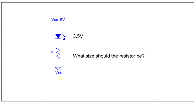
You can see that the voltage across the resistor will be 5v-3.5 = 1.5V. So what size does the resistor need to be to make the current be 20mA? From Ohms Law (V=IR or R=V/I) you need the R=1.5V/20mA=75Ohms.
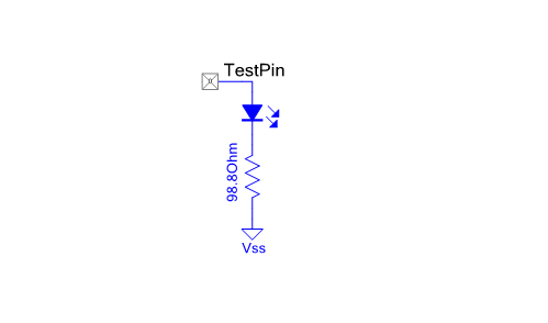
The next thing that I did was build a circuit on my bench to test and see how things were working. In the box of parts in my lab I had an LED with a forward voltage of 3V so I calculate that my resistor needed to be 100Ohms.
When I measure (using my Fluke meter) I find out that the parameters of the system are actually:
- Vcc = 4.7 (instead of 5V)
- The LED VF=2.97 (instead of 3.0)
- The R=98.8 Ohms (instead of 100)
- The IAF = 17.5mA (instead of 20)
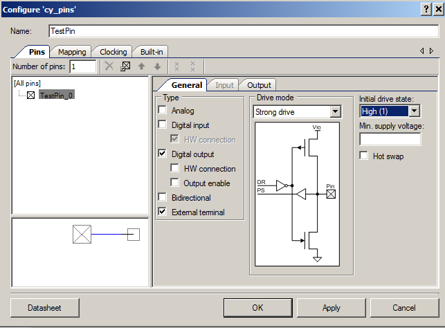
OK. All of that makes sense. The next step in building the blinking LEDs is to drive the same circuit with a PSoC pin just to make sure everything is still OK. To do this I build a schematic in PSoC Creator that looks like this:
And I configure the GPIO like this:
- Select “Initial drive state: High” which means that the pin will start at Vcc
- Select “External terminal” so that I can draw the whole circuit on the outside of the PSoC using the annotation components
When I program the project and measure the output I get:
- VF=2.9V
- VR=1.35
- IAF=13.7mA = 1.35V/98.8Ohm
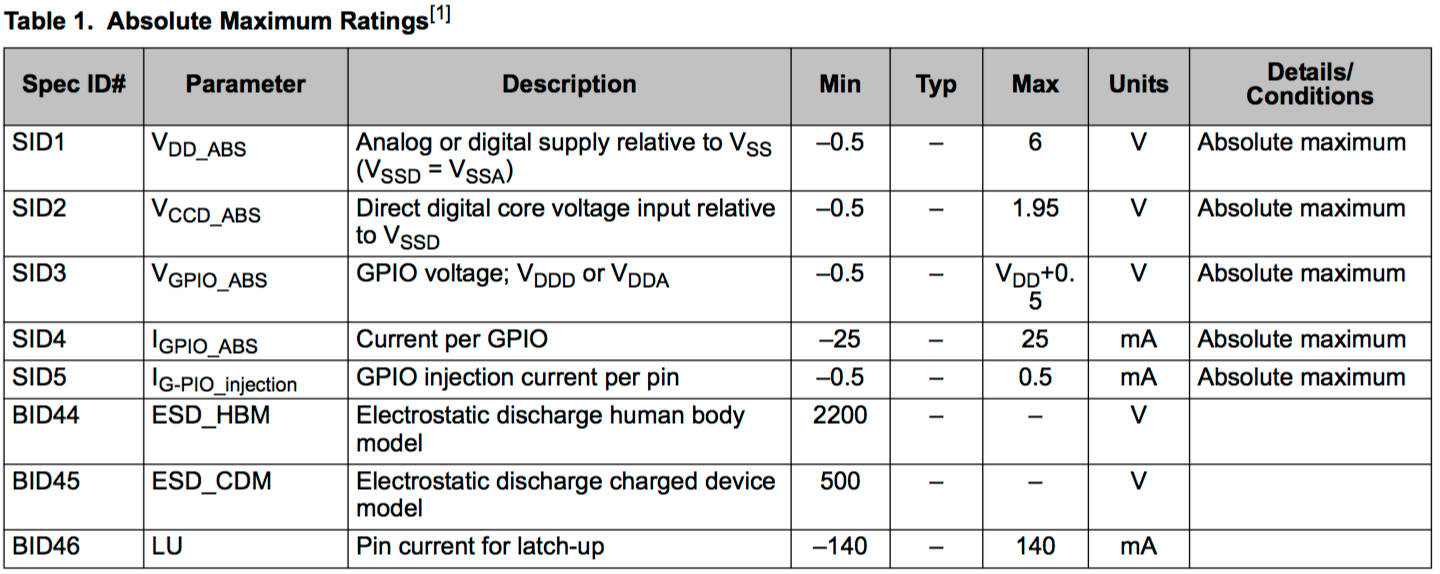
These results are confusing because VF+VR=4.25V yet when I measured the power supply it is 4.9V. Where did the other 650mV go? When I first took the measurement I was worried for a moment that I had drawn to much current out of the PSoC and something was bad. But there was no smoke so that didn’t explain anything. Still confused as I was drawing only 13mA and the chip is capable of delivering 25mA on a GPIO pin. Here is a snap from the PSoC data sheet where you can see SID4 is 25mA.
The bottom line is 13mA < 25mA so if to much current isn’t the problem then what it is? The answer is that the output impedance of the chip is not 0. What is “output impedance”? Inside of the chip there is an PMOS transistor that is used to drive the “1” (or an NMOS for “0”) onto the output pin of the chip (the circuit on the left side of the picture). When this transistor is On and you are driving a 1 onto the output pin, a good model for the on PMOS transistor is a resistor (the equivalent circuit on the right)
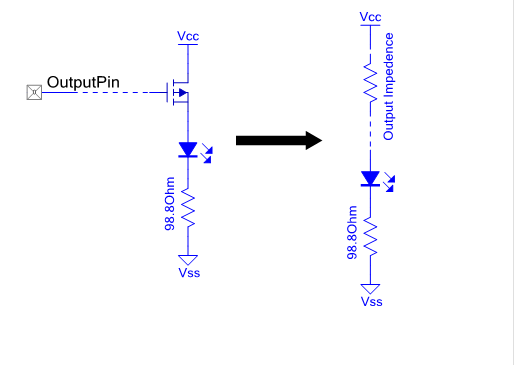
In the case of my circuit the output impedance (from Ohms Law) must be
R = 0.65v / 13.7mA = 47.7 Ohms
OK that is curious. The next question is what is the output impedance of the pulldown transistor? To find the answer I build the same circuit except using a pulldown in the PSoC and powering it with the VCC directly. In fact I built all 4 combinations (power from the VCC, ground from the ground, power from the chip and ground from the chip).
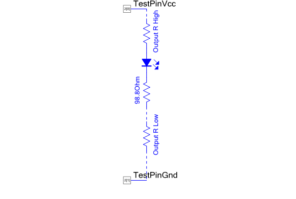
Here is the table of results.
| Configuration | V(VCC-LED) | VF | VR | V(R-GND) | Total | Act VCC-GND | IAF | Rhigh | Rlow |
|---|---|---|---|---|---|---|---|---|---|
| Only Pullup | 0.65 | 2.90 | 1.35 | 0 | 4.91 | 4.9 | 13.7 | 47.7 | 0 |
| Pullup and Pulldown | 0.62 | 2.88 | 1.26 | 0.13 | 4.90 | 4.9 | 12.8 | 48.9 | 10.2 |
| Pulldown Only | 0 | 2.95 | 1.60 | 0.17 | 4.71 | 4.7 | 16.2 | 0 | 10.5 |
| No PSoC | 0 | 2.97 | 1.73 | 0 | 4.7 | 4.7 | 17.5 | 0 | 0 |
Does all of this make sense? What does the data sheet say? It turns out that the data sheet does not specify the output impedance. Instead, it give the worst case output voltage for a high and a low AT a given current and VCC spec. From the spec SID59 (data sheet below) you can see that the worst case Voh is -0.6v at Ioh=4mA and 3V VDD. That spec says that IF you power the chip at 3V AND you draw 4mA out, then the “high” or “1” output will be NO LESS than 2.4V. This is another way of saying that the output impedance of that condition is no worse than 0.6V/4mA = 150 ohms.
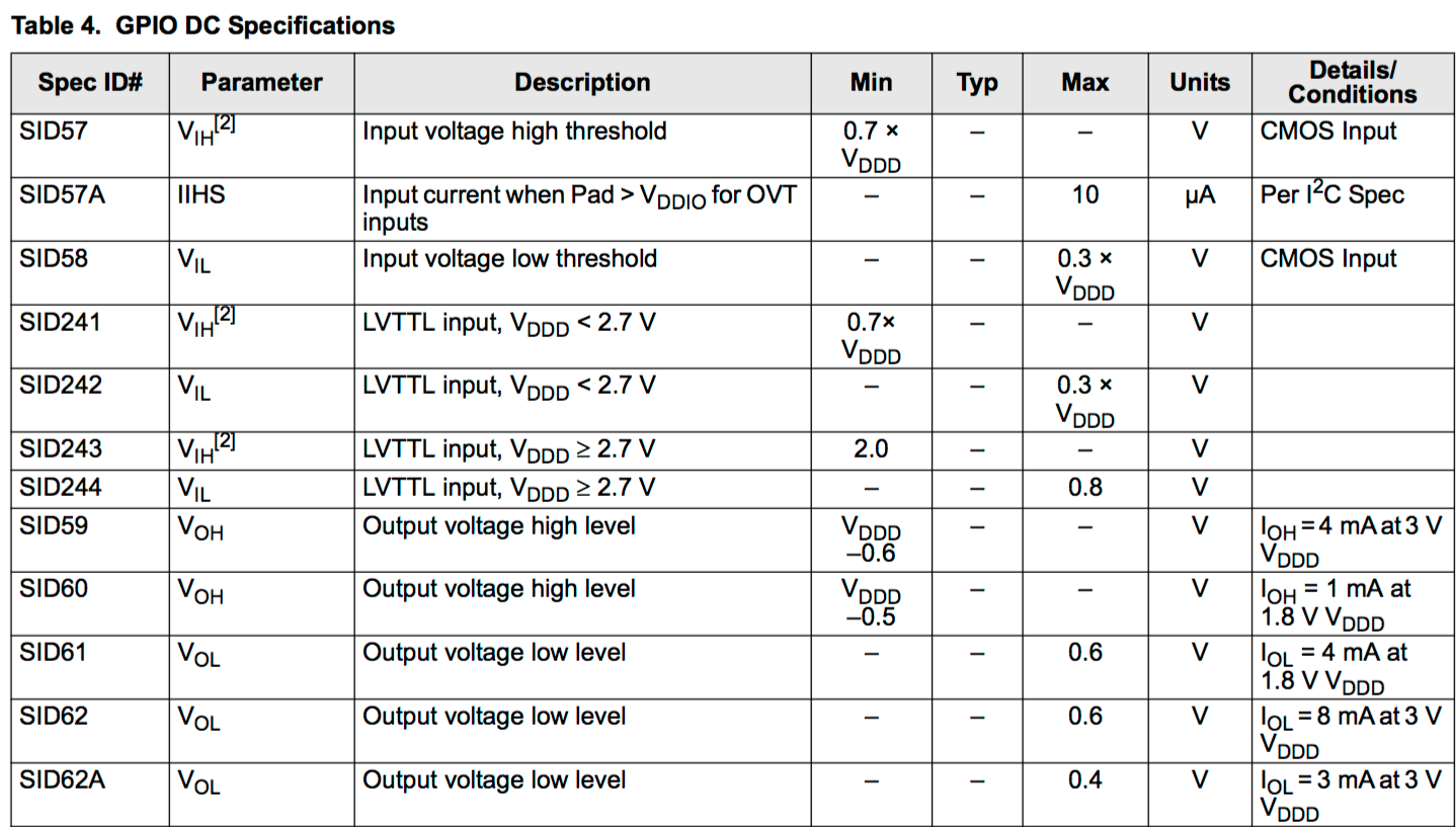
Why is Voh specified as a worst case current/voltage combination? The basic answer is the output buffer has a transistor, actually several transistors, driving the output. The actual V/I characteristic of a transistor is not as simple as just a resistor and it depends on the voltage of the gate, source, and drain. But this would be too much complexity to publish and is unneeded as GPIOs are used to drive logic signals outside of the chip. In the digital output situation you just need to insure that the HIGH output has a high enough voltage to be a logic 1 and that a LOW output is low enough to be a logic 0. In a normal system, logic signals do not require very much current-generally <1mA so 4mA is a worst case scenario.
In the next post I will talk in detail about how to turn 8 GPIO Pins into 16 outputs.
You can find all of the source code and files at the IOTEXPERT site on github.
Index
Description
Pinball: Newton's Attic Pinball
An introduction to the project and the goals
Pinball: Lotsa Blinking LEDs
Everyone needs a bunch of LEDs on their Pinball Machine
Pinball: Matrix LEDs (Part 1)
Saving PSoC pins by using a matrix scheme
Pinball: Matrix LEDs (Part 2)
Solving some problems with the matrix
Pinball: Matrix LEDs Component
How to turn the Matrix LED into a component
Pinball: A Switch Matrix
Implementing a bunch of switches
Pinball: Switch Matrix Component (Part 1)
The switch matrix component implementation
Pinball: Switch Matrix Component (Part 2)
The firmware for matrix component
Pinball: Switch Matrix Component (Part 3)
Test firmware for the matrix component
Pinball: The Music Player (Part 1)
The schematic and symbol for a Music Player component
Pinball: The Music Player (Part 2)
The Public API for the Music Player component
Pinball: The Music Player (Part 3)
The firmware to make the sweet sweet music
Pinball: The Music Player (Part 4)
The test program for the music player
Pinball: The Motors + HBridge
Using an Bridge to control DC Motors
Pinball: The Eagle Schematic
All of the circuits into an Eagle schematic
Pinball: The Printed Circuit Board 1.0
The first Eagle PCB layout of the printed circuit board
Pinball: The PCB Version 1.0 Fail
Problems with the first version of the Eagle PCB layout
Pinball: PCB Layout 1.2 Updates using Eagle
Fixing the errors on the first two versions of the Eagle PCB
Pinball: Assemble and Reflow the 1.2 PCB
Assembling the Eagle PCB
Pinball: Testing the Eagle PCB
Firmware to test the newly built Pinball printed circuit board
Pinball: Debugging the Motor Driver
Fixing the motor driver PSoC project
Pinball: Hot-Air Reworking the Accelerometer Solder
Using a Hot-Air Rework tool to reflow a QFN
Pinball: Debugging the LM317 Power Supply- A Tale of Getting Lucky
Debugging the LM317/LM117 power supply
No comment yet, add your voice below!