The Lost Art of Assembly Language Programming

Cypress introduced it’s first mass market microcontroller in 2001. It used a Cypress designed 8 bit CISC processor running at 24 MHz, with as little as 4 KB Flash and 256 bytes RAM. Wrapped around that was a neat array of programmable analog and digital blocks. This may not sound like much, but with a creative mindset you could get these parts to do amazing things. For instance, I once implemented a complete ultrasonic ranging sensor with full wave analog demodulation in a single PSOC1 as shown below.

PSOC1 Ultrasonic Ranging

With CPU resources at a premium, you had to write tight, efficient code to get the most out of PSOC1. A single C library could consume the entire Flash. Consequently, I wrote a lot of assembly code. That’s not so bad, since I actually enjoy it more than C. There’s a certain elegance to well written, fully commented machine code. In the case of PSOC1, here’s what you had to work with: 5 registers, some RAM and Flash. That’s it. Real Men Write In Assembly.
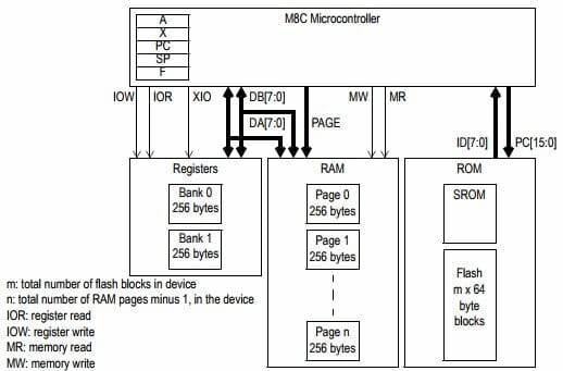
M8C Architecture


We’ll start with simple machine code instruction to make the CPU do something. You can reference the M8C assembly language user guide here for more details. To get the M8C to execute 2+3=5 we write:

mov A,2       ;Load A with 2
add A,3       ;Add 3 to A. Result=5 is in A

We can get fancy by using variables. Let’s add R=P+Q. Assume P is at RAM location 0x20 and Q is at location 0x21, and R is at 0x22

;Initialize variables
mov [0x20],2  ;Load P with 2
mov [0x21],3  ;Load Q with 3

;Add variables
mov X,[0x20]  ;X <- P
mov A,[0x21]  ;A <- Q
adc [X],A     ;X <- P + Q
mov [0x22],X  ;R <- X

The fun thing about assembly is you can always dream up cool ways of doing things in less operations based on the machine’s instruction set. For example, we can simplify the above code as follows:

;Add variables
mov [0x20],[0x22]   ;R <- P
adc [0x22],[0x21]   ;R <- P + Q

In my experience, a good programmer with expert knowledge of the instruction set and CPU resources can always write better code than a compiler. There’s a certain human creativity that algorithms can’t match.

All that being said, I had not seen a good “machine code 101” tutorial for writing assembly in PSOC Creator on modern ARM M0 processors. So let’s walk through one now. We’ll use a CY8CKIT-145 and blink the LED. It’s just what happens to be laying around on the lab bench. Any PSOC4 kit will do.

CY8CKIT-145-40XX

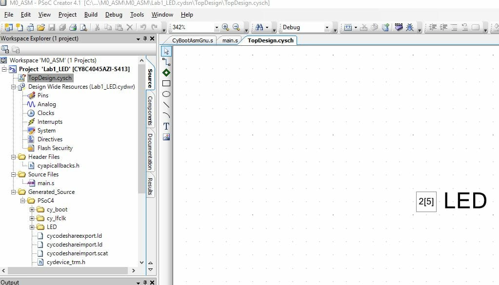
We’ll start by creating a standard project in PSOC Creator, drop a Digital Output pin on the schematic and call it “LED”

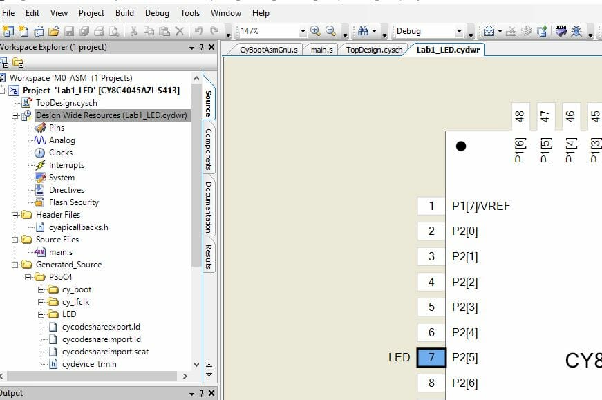
Then open the .CYDWR file and drag pin LED to P2[5], since that’s where it is on the LED board. Yours may be in a different place on whatever board you are using.

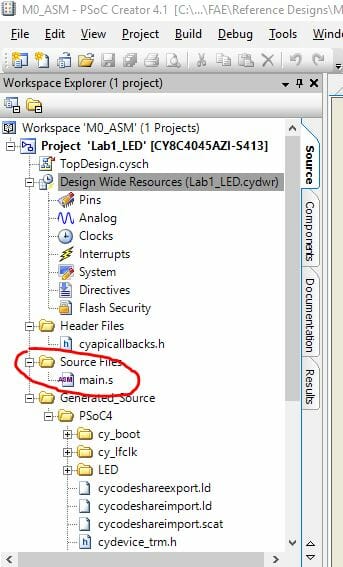
Now under “Source Files” in the workspace directory you will delete main.c and replace with main.s

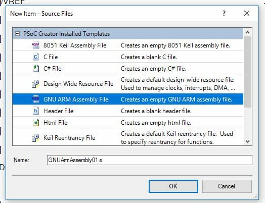
Now right clock on “Source Files”, select “Add New File” and select “GNU ARM Assembly File” in the dialog. Rename the file from GNUArmAssembly01.s to main.s

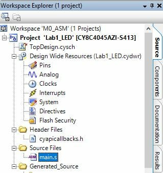
Your workspace ends up looking like this:

So far, so good. Now open main.s, delete everything if it’s not empty and add the following code. This sets up the IDE for M0 assembly architecture

// ==============================================
// ARM M0 Assembly Tutorial
//
// 01 – Blink LED
// ==============================================
.syntax unified
.text
.thumb

Next we need to include register definitions for the chip we are using. These are all from the PSOC4 Technical Reference Manual (TRM)

// ==============================================
// Includes
// ==============================================
.include “cydevicegnu_trm.inc”

Then we are going to do some .equ statements, same as #define in C. This identifies the Port 2 GPIO data register plus bits for the LED pin in on and off state

// ==============================================
// Defines
// ==============================================
.equ LED_DR,CYREG_GPIO_PRT2_DR          // LED data reg address
.equ LED_PIN,5                          // P2.5
.equ LED_OFF,1<<led_pin                 // 0010 0000
.equ LED_ON,~LED_OFF                    // 1101 1111

Now you add the right syntax to set up main()

// ==============================================
// main
// ==============================================
.global main
.func main, main
.type main, %function
.thumb_func

Finally we add the code for main, which is pretty simple:

main:
ldr r5,=LED_DR      // Load GPIO port addr to r5

loop0:
ldr r6,=LED_ON      // Move led data to r6
str r6,[r5]         // Write r6 data to r5 addr

ldr r0,=0xFFFFFF    // Argument passed in r0
bl CyDelayCycles    // Delay for N cycles

ldr r6,=LED_OFF     // Move led data to r6
str r6,[r5]         // Write r6 data to r5 addr

ldr r0,=0xFFFFFF    // Argument passed in r0
bl CyDelayCycles    // Delay for N cycles

b loop0             // Branch loop0

.endfunc            // End of main
.end                // End of code

One thing to note: The function CyDelayCycles is defined CyBootAsmGnu.s. Any function in assembly gets its arguments passed by the first 4 registers r0,r1,r2 and r3. Before calling the function you simply load r0 with the argument then do a bl (branch with link). This is also why I avoided the first 4 registers when messing with LED data. If you’re interested in doing more with ARM assembly, definitely read the Cortex M0+ Technical Reference Manual. It’s a great primer for the M0+ instruction set.

That’s it. End result is a blinking LED. Cool thing is you can use PSOC Creator with all it’s nice features, but sill access the power of machine code.

You can get the project ZIP file here.

Regards
Darrin Vallis
Serial Wire View with PSOC4

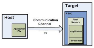
I use PSOC4 to invent all kinds of unique solutions for customers. Usually, they want them field upgradeable to deploy new features or fix bugs. Fortunately Cypress has a great I2C boot loader to meet this need, so I use the heck out of it.
Cypress has a great debugger built into PSOC Creator which fully supports all the ARM Serial Wire Debug protocols such as breakpoints, single step, memory, register viewing etc. However, when you are running a boot loader the debugger does not work! Why not? Because with a boot loader there are two applications resident in PSOC4: The boot loader and application. This is not supported by Cypress implementation of SWD.
Where does this leave you, the intrepid code developer, when debugging a boot loader project? Personally, I have used all kinds of methods: debug UART interface, debug I2C interface, bang out states on pins, debug Bluetooth interface … and on and on. You get the idea. All these methods burn a communications interface and require extra pins on the chip. Sometimes that’s not possible.

The issue recently came to a head when a customer very nearly in production experienced a boot loader failure. One system out of a few thousand was “bricked” when they tried to field  update in the lab. Their pinout is frozen, they can’t add new hardware so how do we look inside PSOC4 and see what’s going on?

I woke up at 2 AM and thought “Ah Ha! SWV!” (Yes, I Am A Geek) Serial Wire View is an ARM native debug protocol that let’s you XRAY the insides of any ARM MCU with the right interface. SWV is a protocol which runs on the SWD pins (clock and data) but also needs the Serial Wire Output (SWO) pin. Cypress left the SWO pin and associated IP off of PSOC4 to save die cost, foiling my great idea. Brief interlude to drink and bang head on desk.

Fortunately, I don’t give up easily. At least my subconscious does not. Woke up the next night thinking “Ah Ha!” again. Wife was mildly annoyed, but tolerates my idiosyncrasies.

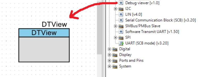
Cypress has a nice software UART transmitter implementation. I shamelessly stole it, modified for my purposes and created a custom component. (It’s pretty easy to do this by the way) Baud rate was modified to 230 KBps and the output pin forced to a specific pin with a control file.

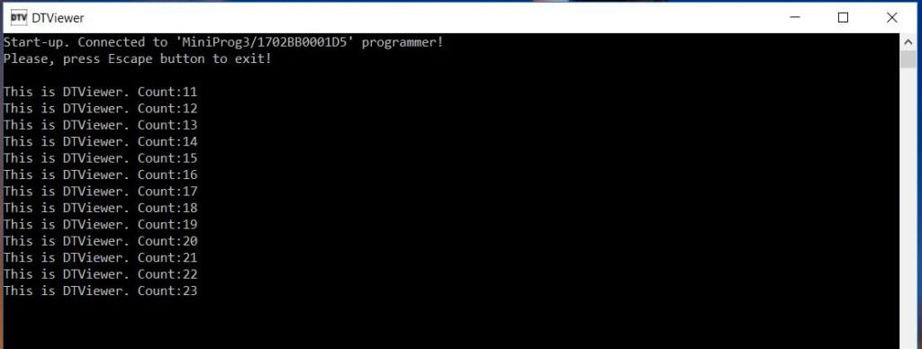
Once the component is in place, you can use its _DView_Printf( ) API call to display any debug data. Here is an example:

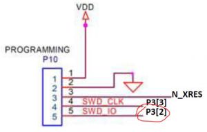
More about that output pin. Cypress sells a tool for programming and debugging PSOC called CY8CKIT-002, aka MiniProg3. The programming connector consists of VDD, GND, reset, SWD clock and SWD data as shown below.

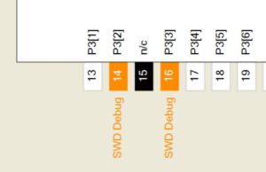
Since we can’t use SWD protocol for debugging anyway, we can change the pins from SWD to normal GPIO. The pins still function for programming. By default they are in SWD mode as shown.

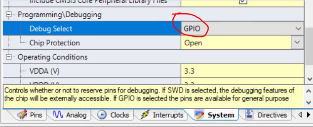
Going to the system tab of the .CYDWR file, we can change them to GPIO.

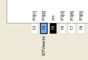
Once we do that, the pins look like this. Here’s the trick. We now assign the TX output of our DTView component to pin 3[2], which is available  on the SWD programming header, pin 5.

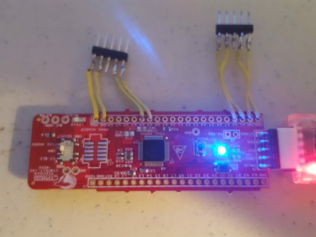
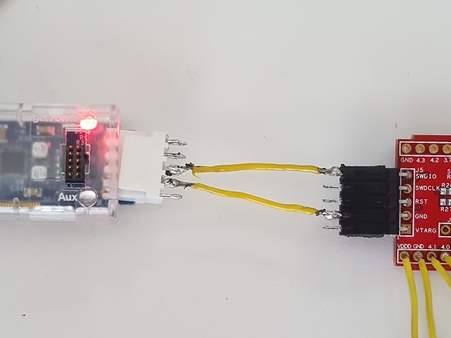
Can you see where we are going with this? Printf( ) data is now coming out of PSOC4 on pin 3[2], easily accessible on our debug header. This is where MiniProg3 comes in. It can actually receive data as a 230 KBps RX UART on its XRES pin. Weird, right? By building a simple interface cable we can get the data from your debug header into MiniProg3.

MiniProg3 XRES —— SWD HEADER pin 5

MiniProg3   GND —— SWD HEADER pin 2

However, MiniProg3 does not show up as a COM port on your PC, so how do we the data? It needs to be accessed by a host application running the PP_COM API. This is documented under PSOC Programmer Component Object Model COM Interface Guide, Cypress specification 001-45209. If you installed PSOC Creator or Programmer, this document is actually on your PC under C:\Program Files (x86)\Cypress\Programmer\Documents. Engineers don’t like to read instructions. Amazing what you can find when you do.

I wrote a simple  console application which opens MiniProg3 using PP_COM, retrieves data from the serial RX pin via USB and displays it like a simple terminal program. Voila! You now have a serial debugger that works for any PSOC4 project using MiniProg3 as your USB to serial dongle.

Customer was really happy with this. We were able to immediately see his problem and fixed it in about 5 minutes.

Finally, here are all the source files

DTView Firmware : PSOC Creator example project and DTView component

DTViewer Binary : Installer for DTViewer console

ViewerSource : Complete source code for DTViewer console (Requires Visual Studio 2015)

That’s all. Have fun with the new debugging tool.

DTV

PSoC4000s & The SmartIO – Part 1

In the previous four posts I talked about building an IOT device using the new CY8CKIT145.  You might remember from the first post that my original objective in picking up the board was to try a new feature of PSoC Creator.  Well, over the last few days I have been trying out that feature. Actually, it isn’t a feature of the software, it is a feature of some of the new chips called the Smart IO.  The Smart IO is a programmable logic bock that sits between the High Speed IO Matrix (HSIOM) of the chip and the Input/Output Port.  The HSIOM has all of the peripherals (SCB, TCPWM etc) of the chips attached to it.  The Smart IO will allow you to take signals from inside or outside of the chip, perform logic functions on them, and then drive those signals into or out of the chip.  Some of examples of why you might want to do this include:

  • Combining several inputs (from the outside) to trigger an interrupt
  • Inverting a signal entering the chip
  • Inverting a signal exiting the chip
  • Remapping an input from one pin to a different input (e.g. flipping Tx, Rx pins)
  • Buffering one signal into multiple output pins (to increase the drive strength)

As usual with Cypress programmable logic, you can do a jaw dropping number of clever things.  This block includes sequential logic as well as combinational logic, so it is possible to make state machines in the fabric.  It also includes more surprises which have not been shown yet.

The Smart IO works the same as other peripheral blocks, you start by dragging the component onto the schematic and double clicking to start the customizer.

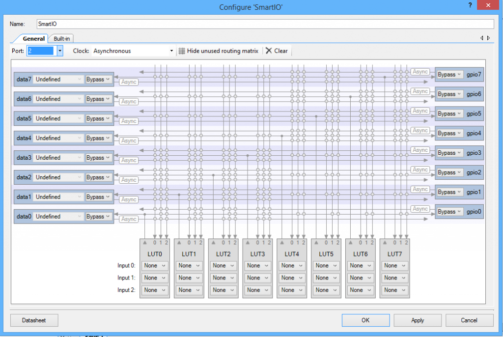
When you start the customizer you get the screen below.  The first thing to decide is which Port is going to use the Smart IO.  The Smart IO completely takes over an entire port.  On this chip there are two Smart IOs, one on Port 2 and one on Port 3.   When you look at the customizer there are some things to notice:

  • On the right side of the customizer you can see the 8 GPIO pins.  The dropdown menus that are currently labeled “Bypass” allow you to select the mode of the pin (Bypass, Input, Output, None).
  • On the bottom of the customizer you can see the 8 LUTs and select their inputs.
  • On the left side of the customizer you can see the the 8 connections to/from the HSIOM.  The drop down menu that is currently labeled “Bypass” allows you to select the mode of that connection to the HSIOM (Bypass, Input, Output, None).   I will talk about the “Undefined” menu in the with the next picture
  • In the middle of the customizer is the routing matrix.  Horizontally on the routing matrix there are 8 groups of three wires.  The top wire in each group is a wire that originates with the GPIO.  The middle wire originates from the corresponding LUT.  The bottom wire originates from the HSIOM.  For example the top three wires in the picture are
    • Line 1: from GPIO7
    • Line 2: from LUT 7
    • Line 3: from Data7
  • You can “make” the connection by either by clicking the solder dot or by choosing from the coresponding drop down menu (more on that below)

basicsmartio

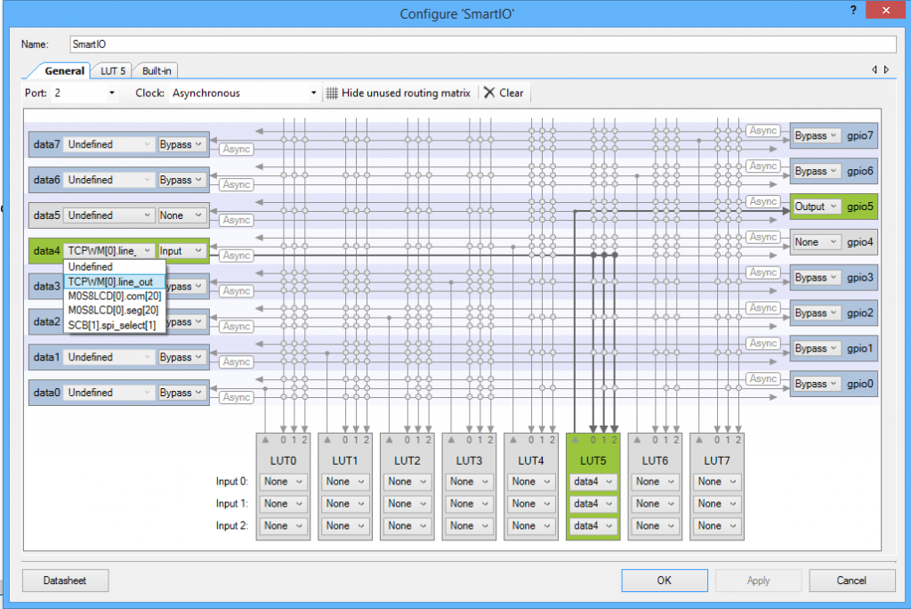
The other menu on the HSIOM side of the customizer says “Undefined”.  This menu has a list of each fixed function device and the inputs/outputs of that device that can be connected to that input/output.  This menu doesn’t actually change anything in your design, it is only for information.  For example you can see in the screen shot below that  data4 can connect to:

  • TCPWM0: Line_Out
  • LCD0: COM[20]
  • LCD0: SEG[20]
  • SCB1: Spi Select[1]

smartio-dataselect

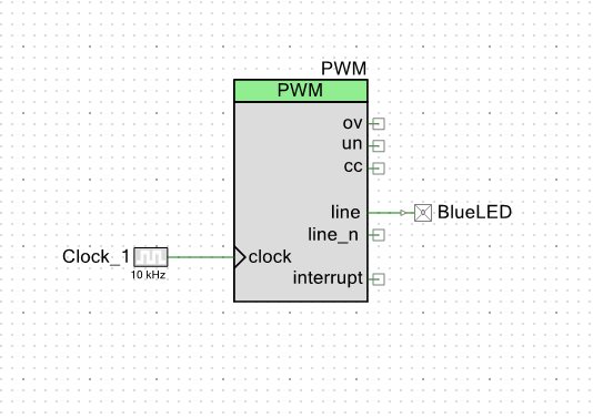
The best way to show you how all this works is with an example.  One of the frustrating things for me in the PSoC 4 Family has always been that the fixed function blocks (TCPWM, SCB) are only allowed to connect to a few pins on the chip.  This can be a bit of a pain if you have a board that is already wired and you need to remap a pin.  Take for example, on the Cy8CKIT-145 the user LED on the main board is connected to P2[5].  If I want to drive that LED with the Line out (instead of the Line_Out_N) I would create a schematic like this:

BlueLEDSchematic

When I go to the DWR to assign the pins I would see that the BlueLED cannot be attached to P2[5].  You can see all of the legal placements of that pin because they are highlighted in green.

blueledpinassignment

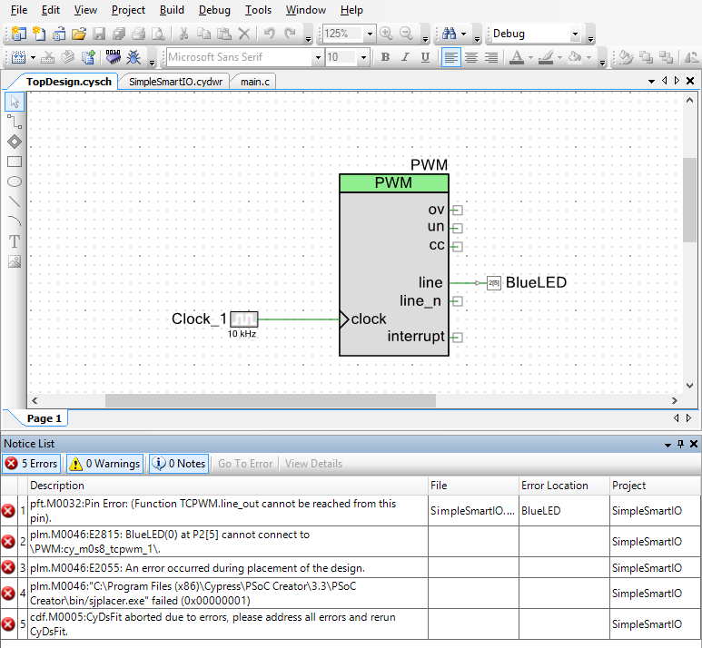
If I try to do it anyway, I will get the following error when I build.

pwm_error

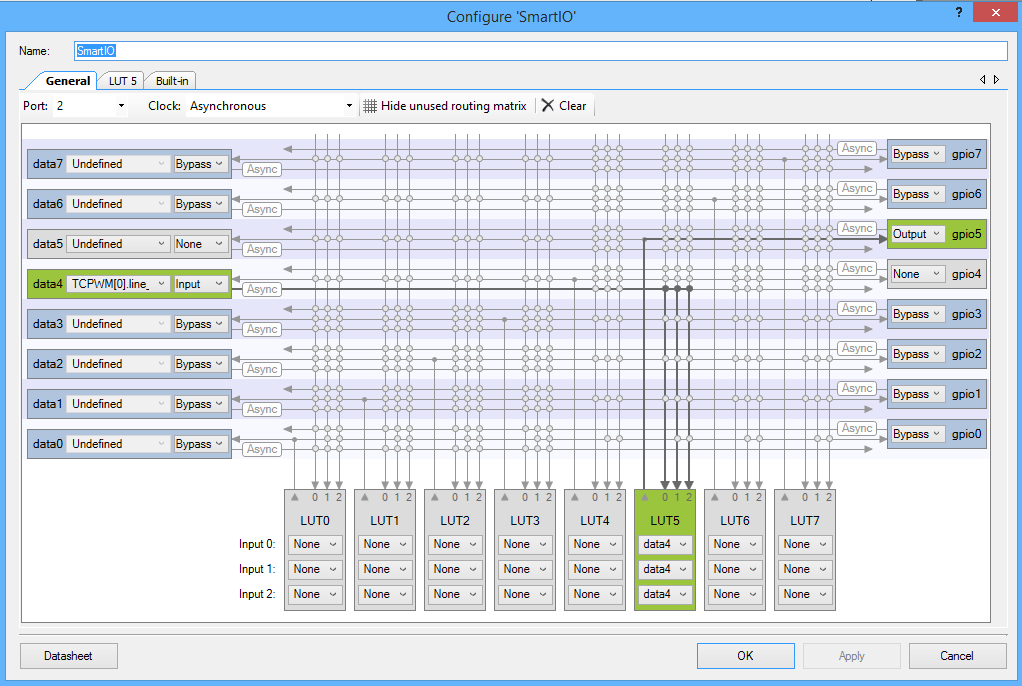
This error says that I cannot connect the “line” output of the TCPWM to P2[5] (the pin with the LED).  That sucks.  But, with the Smart IO, I can “remap” the TCPWM Line output to P2[5].  To do this, I will start with a by adding a SmartIO to my schematic and configuring it.

  1. Select Port 2
  2. Configure GPIO 5 to “Output”.  This can be done by either clicking on the “solder dot” or by selecting output from the drop down menu
  3. Select data 4 as “Input”
  4. Select data 4 as “TCPWM[0].line.  Remember that this is ONLY for your information and doesn’t actually change anything in the project.
  5. Select the 3 inputs to LUT5 to be the data4 line which can be done from the three drop down menus or by clicking the three corresponding solder dots.

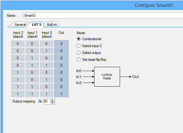
Screen Shot 2016-03-06 at 9.53.10 AMNext, I configure the LUT to “passthrough” by setting up 000 = 0 and 111=1 (which are the only two possible combinations as the three inputs are tied together).  You change the “Out”s from 0->1 and 1->0 by clicking on it.

LUT5

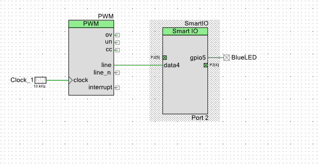
Then I will re-wire up the schematic to look like this:

blue-led-schematic-smartio

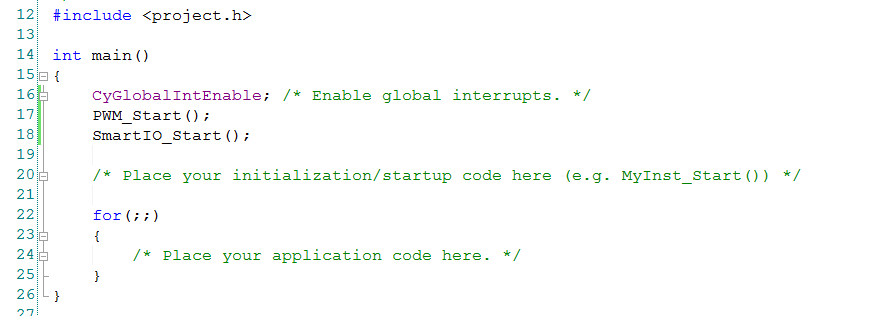
The firmware is trivial,  just start the PWM and the SmartIO

blue-led-firmware

When I program the kit the blue LED starts blinking.  Cool.

In the next posts I will teach you how to use some other configurations of the Smart IO and how to use the CapSense block to create inputs for the Smart IO.

You can find this PSoC Creator workspace on github in the directory called “SmartIO”.  This project is called “SimpleSmartIO”.

Index Description
PSoC4000s & The SmartIO – Part 1 An introduction to the SmartIO and first project
PSoC4000s & CSX Mutual CapSense Buttons Part 1 Using mutual capacitance
PSoC4000s & CSX Mutual CapSense Buttons Part 2 Using the CapSense tuner
PSoC4000s & The SmartIO – Part 2 A 3 input XOR logic gate
PSoC4000s & The SmartIO – Part 3 A 3 bit up counter state machine
PSoC4000s & The SmartIO – Part 4 Using an external clock with the Smart IO
PSoC4000s & The SmartIO – Part 5 Triggering an interrupt

PSoC4000s and the CY8CKIT145 Stamp Board – Part 4

OK.  We’re ready for the big moment: the user test.  I was feeling pretty cool.  I had spent the week talking to 100s of people and putting on a pretty good show.  I was the master of all things PSoC, a geek rockstar.  So I programmed the firmware.  The slider worked.  I was able to connect to the PRoC BLE from my app.  But for some stupid reason the the PSoC and PRoC just were not talking and I had no idea why.  And to make matters worse, I didn’t have anything I could (easily) use to debug the problem.   So much for being the king of PSoC.  I assumed that I had firmware bugs. I tried a bunch of different things, single stepping code, trying different pins, etc.  But nothing worked.  I couldn’t figure it out.  It was intensely frustrating to be stuck on the airplane with a broken design.

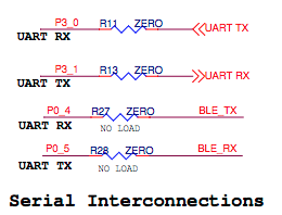
As soon as I landed in Detroit, I logged in to get my email.  I looked for messages from Rajesh (the PSoC Kit Manager) and sure enough, he had emailed me the missing schematic.  After digging through the schematic, I found the error.

schematic-resistors

The connection between the PRoC and PSoC had a 0 Ohm resistor that was “No Load,” meaning the footprint was there, but the board manufacturer had not put on the resistor.  This was done so that the pin could be used as a GPIO for something else.

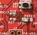
Here is a zoomed-in picture of the PCB:

missing-resistors

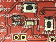
The good news was, I was only one plane ride and an hour drive from my soldering iron.  As soon as I walked in the door, I went straight to my lab.

fixed-resistors

Now everything works.

There are two morals to this story:

  1. Don’t go to immediately to your lab after being gone for a week, as it really irritates your wife.
  2. Look closely at the schematic.

You can find the PSoC Creator workspace on github in the directory called “capsenseble-145.”

PSoC4000s and the CY8CKIT145 Stamp Board – Part 3

In this post, I will take you through the PRoC BLE schematic and firmware.  I describe a very similar version to this in great detail in the video you can find on the Cypress Video Training website.

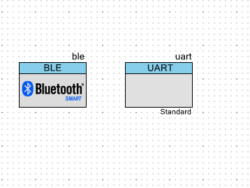
First, I create a new project in my workspace called “145capsenseled-ble.”  Then, I add the UART component (the SCB version) and the BLE component.

schematic

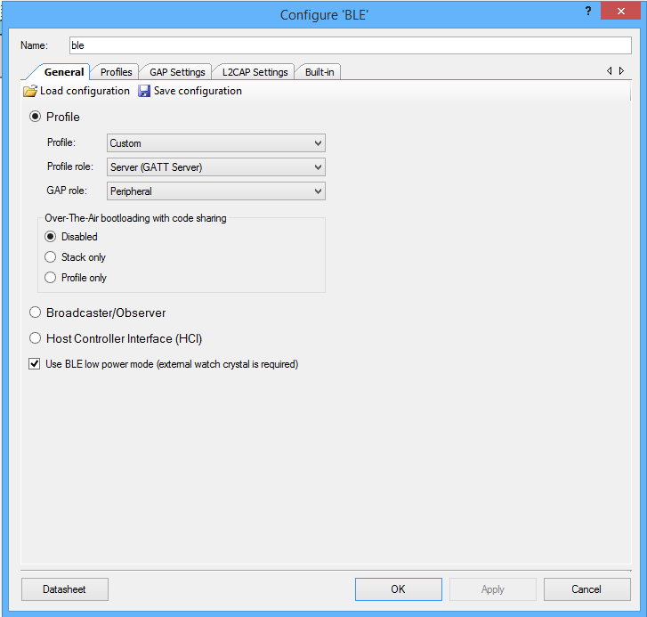
Next, I configure the component to be a GATT server with a custom profile and a GAP client.

overall-profile

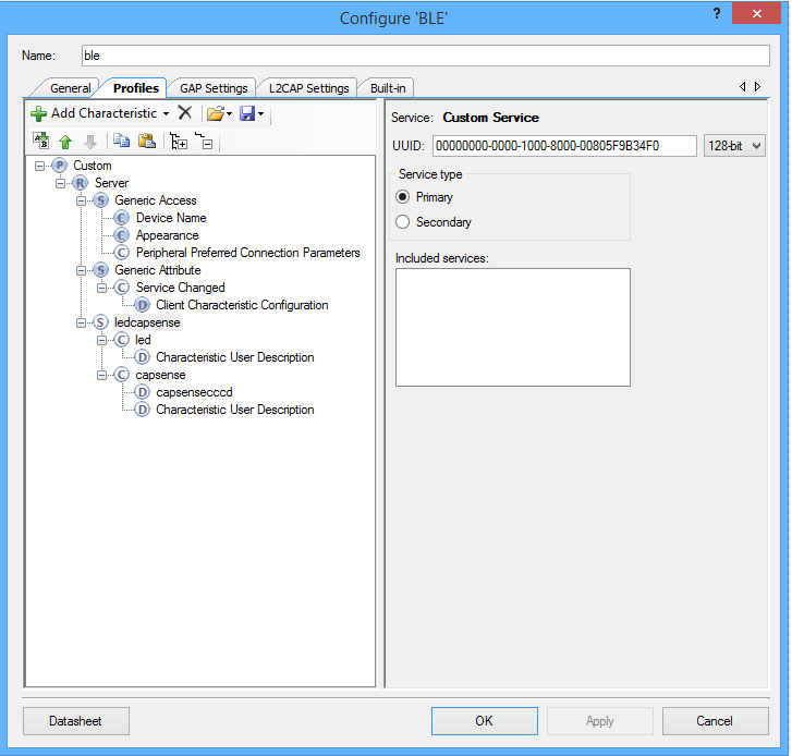
Then I create a custom service with two characteristics:

  • The “led” characteristic, which is set up as a uint8 that is writeable and readable.
  • The “capsense” characteristic, which is set up as uint16 that is readable and has a “notify.”

Next, I configure the UUIDs of the service and characteristics to match what is hard-coded in the iOS app.  Then, I add “Client User Descriptions” that describe the characteristics in plain text.

gatt-settings

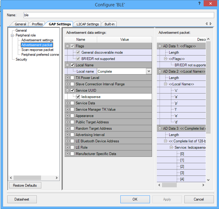
Next I configure the GAP settings, specifically the advertising packet.

advertising-packet

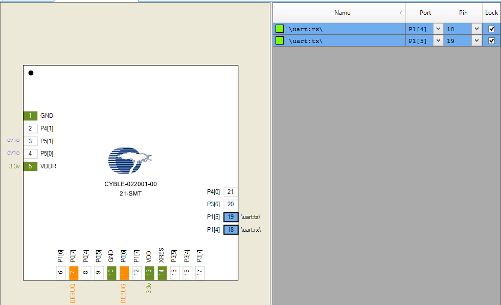
I make the pin I assignments, which is just the UART Rx and Tx lines.

dwr-pin-assignment

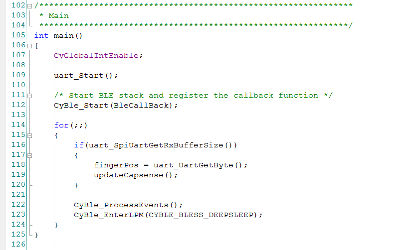
Finally, I write the firmware.  I started with main.  In the infinite loop (line 116), if I have received a byte from other side, then I assign it to the global variable “fingerPos” (line 118). Next, call updateCapsense() (line 119), to update the GATT database with the new value of the slider.

main

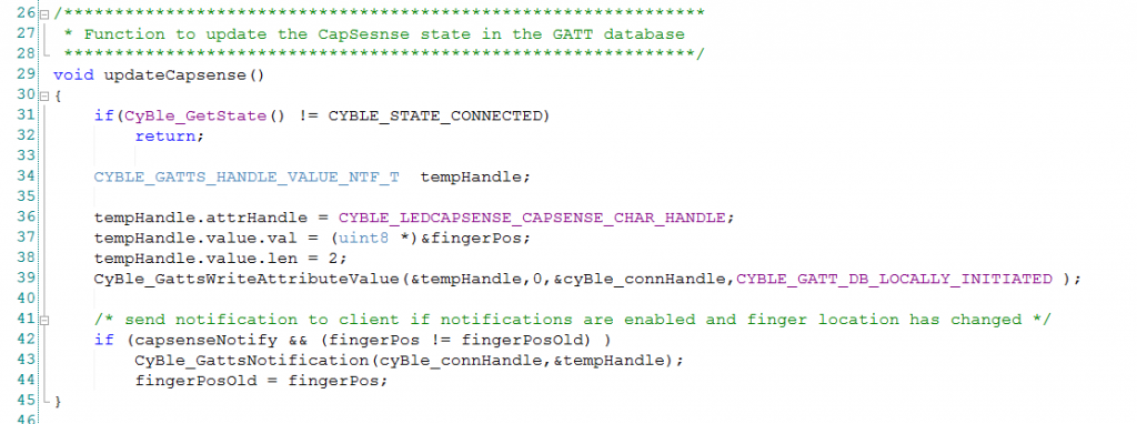
The updateCapsense function:

Lines 31/32 If there is no connection, then don’t update the GATT database.

Lines 33-39 Update the GATT database with the current fingerPosition.

Lines 42-43 If the iPhone side has asked for notification and the position has changed, then send a notification.

Line 44 Save the last position.

update-capsense

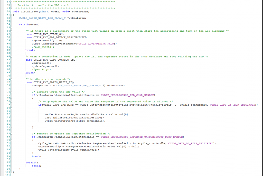
The BleCallBack is the most complicated section of firmware.  It uses a “switch” statement to handle the different event “cases.” The cases are:

  • CYBLE_EVT_STACK_ON & CYBLE_EVT_GAP_DEVICE_DISCONNECTED:  In either of these cases you want to start the advertising function.
  • CYBLE_EVT_GATT_CONNECT_IND: When there is a connection made, update the GATT database with the current state of the CapSense and the LED.  This allows the iOS side to read the correct values.
  • CYBLE_EVT_WRITE_REQ: There are two kinds of write requests that are valid.
    • CYBLE_LED_CAPSENSE_LED_CHAR_HANDLE:  If the remote side writes into the LED value, then send that data to the PSoC4000S via the UART.
    • CYBLE_LEDCAPSENSE_CAPSENSE_CAPSENSECCCD: If the remote side has been asked to notify (or un-notify), then save that in the global variable capsenseNotify.

ble-callback

That is all of the firmware.

In the next post, I’ll take you through the debugging I had to do.

You can find the PSoC Creator workspace on github in the directory called “capsenseble-145.”

PSoC4000s and the CY8CKIT145 Stamp Board – Part 2

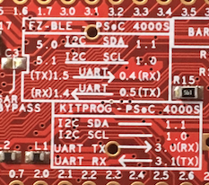
In the previous post, I unboxed the CY8CKIT145 and showed you the schematics.   In this post, I will show you how to build the CapSense firmware that runs on the PSoC4000S.  The first decision I needed to make was how to connect the PSoC and the PRoC chips.  So I looked at the back of the kit and there was a handy-dandy picture of the schematic in the silkscreen.  Here is a zoomed in view:

zoom-145

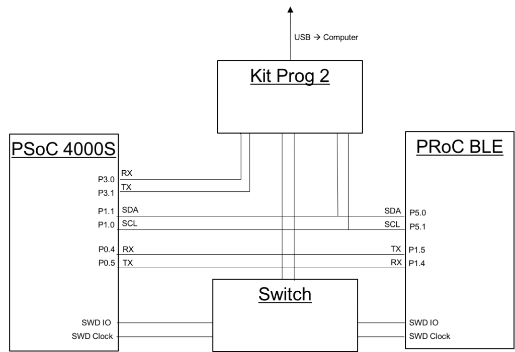
I didn’t have the schematic on the airplane, but here is a more “schematic” view of the chips on the board.

systemschematic-c


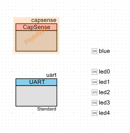
I knew that the UART source code would be slightly easier, so I picked that as the mechanism to connect the chips.  On my computer I had the “capsenseled” workspace from the videos.  So, I created a new PSoC4000S project in that workspace called “145capsenseled.”  I started with the schematic:

  1. Add the new CapSense component.  I am currently running a “nightly build” of PSoC Creator 3.3 that supports the new chip.  You can see in the PSoC Creator release I’m using there is a prototype version of the CapSense component.
  2. Add 5 Digital Output Pins under software control to drive the LEDs that are next to the slider
  3. Add 1 Digital Output pin to drive the blue LED
  4. Add a Serial Communication Block (SCB) configured as a UART

capsenseled-schematic

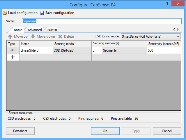
Here is a screenshot of the new CapSense component configuration wizard.  You can see I added a linear slider and set up the component to use SmartSense full-auto tuning.

capsense-configuration

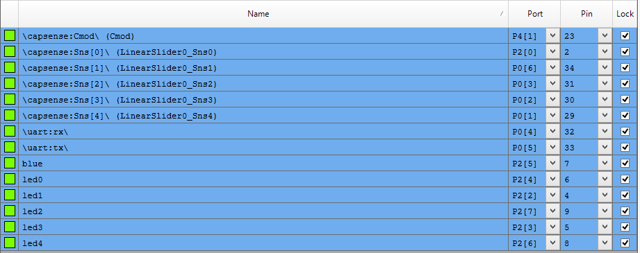
After configuring the CapSense, I set up the pin assignments using the DWR:

capsenseled-pinassignment

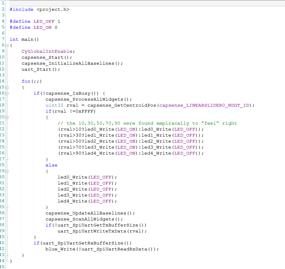
Then I wrote the firmware, which was pretty straight forward.

  • 10-11 start the CapSense
  • 12 start the UART
  • 16: If the CapSense block is done scanning and is idle, then read the CapSense and do something with it (lines 17 -> 41).
  • 18: figure out where the person is touching
  • 19: if they have actually touched the block
  • 22-26 light up the LEDs
  • 30-35 If there is no touch, then turn off the LEDs.
  • 36-37 start the next scan
  • 38-39: If the UART is not busy… then send the position (0-100) or (0xFF if there is no touch).
  • 41-42: If there is a byte in the UART receive buffer, then light up or turn off the Blue LED. (Notice that the LED is active low so I use the “!” operation to flip the state of the signal.

capsense-firmware

After that, I programmed the kit and tested it.  It seemed like everything was good.  In the next post, I’ll show you the schematic and firmware that runs on the PRoC BLE.

You can find the PSoC Creator workspace on github in the directory called “capsenseble-145.”

PSoC4000s and the CY8CKIT145 Stamp Board – Part 1

One of the cool things about my job is I get to try out lots of new development kits before they are released to the general public.  In the previous post I talked about the demonstration I gave at the Embedded World conference using the CY8CKIT-042 BLE.  You can find a complete video tutorial for that project on the cypress.com video tutorial website.  While I was at the conference, I picked up an engineering sample of a new development kit and put it into my backpack because I wanted to try a new feature of PSoC Creator on the way home.  But, when I got on the airplane, I thought I would build the same project I had demonstrated at the conference using this kit.  So, in the next few posts, I am going to show you the new CY8CKIT145 Stamp Board and how to build an IOT solution with it.

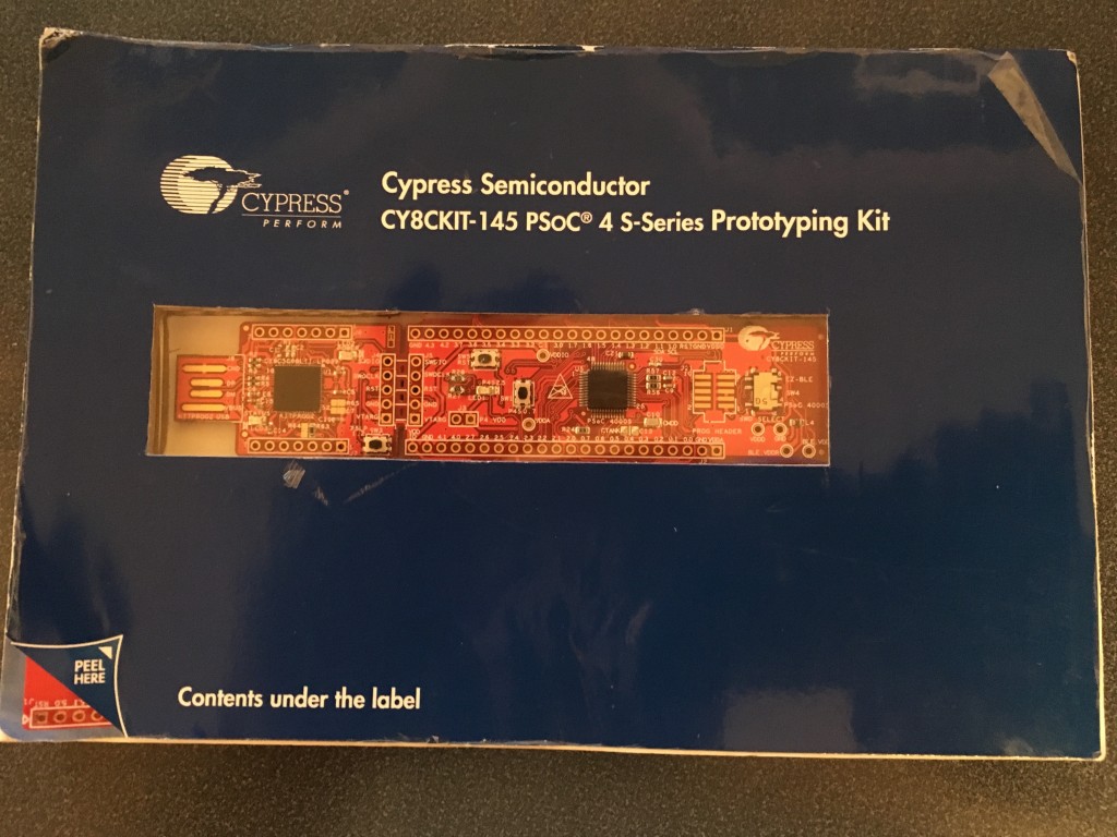
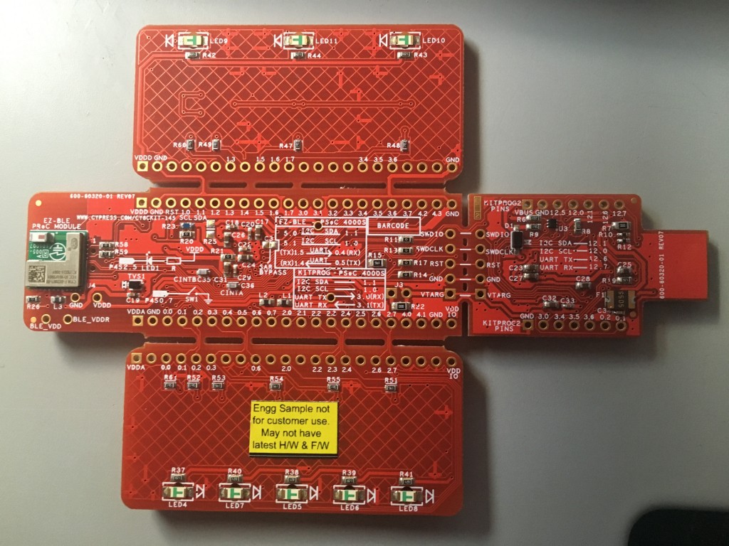
It is called a “stamp board” because it comes in a flat postage stamp-like postcard mailer.  Here is a picture of the front and the back (you can see that it has already lived a hard life riding around in my backpack).

IMG_2720

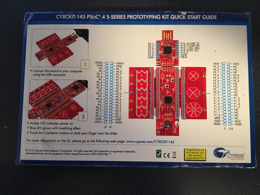
Here is the back of the mailer:

IMG_2722

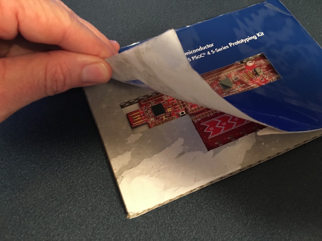
In the picture you can see the yellow label proclaiming this to be an engineering sample.  It doesn’t seem like much, but when you pull back the front of the package you get to see the surprise:

IMG_2721-1

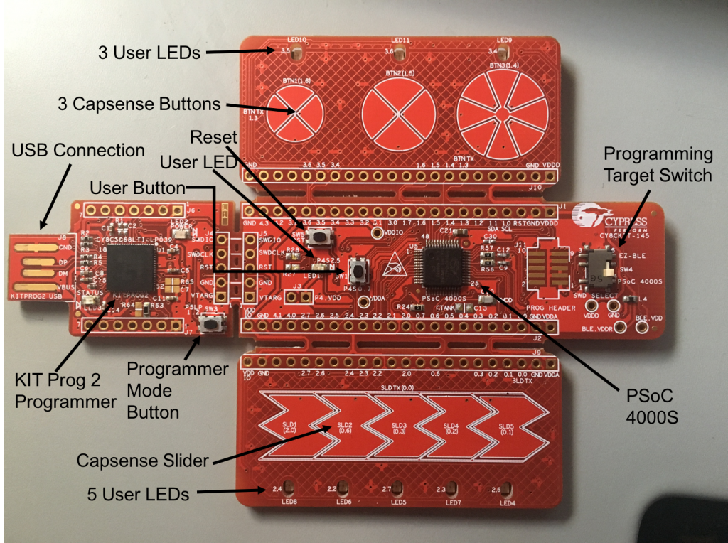
The kit can literally be broken into four separate pieces:

  1. The main board:
    • The PSoC4000S
    • A reset switch
    • A user LED
    • A user push button
    • A programming selector (to pick either the PSoC4000s or the PRoC BLE (that is on the back of the kit)) as the target of the programmer
    • All of the PSoC4000S pins are available on the 100mil center headers
    • A PCB footprint for a 10-pin ARM programming header
  2. A programmer board:
    • A PSoC5LP programmed with KitProg2 Firmware
    • A programmer mode button
    • 100mil center header with some of the PSoC5LP pins
  3. A Capsense slider user interface board with a 5 Segment Slider and 5 LEDs
  4. A Capsense button user interface board with 3 mutual capacitance buttons and 3 LEDs

145front-e

And the back, with the tiny 10mm X 10mm PRoC BLE module:

IMG_2706

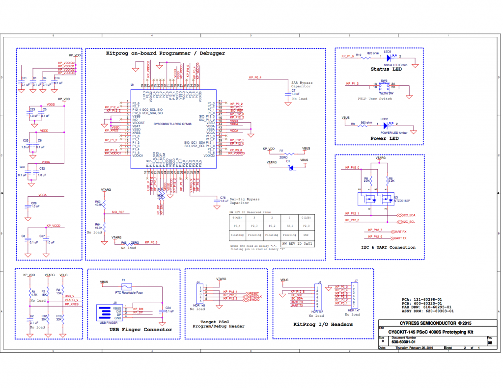
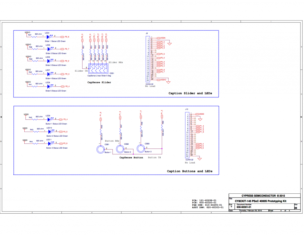
Here is the schematic for the board:

CY8CKIT-145_PSOC_4A-S1-page1

CY8CKIT-145_PSOC_4A-S1 page 2

CY8CKIT-145_PSOC_4A-S1-page3

I wanted to build a project that would have two-way communication between my iPhone and the board, and would be compatible with the Swift App I had written.  The user of the board would have a capsense slider (and LEDs) of which the iPhone App could read the position.  In addition, it would have an LED that the iOS app could turn on and off.  Here is a demonstration that I filmed with my iPhone on the airplane:

In the next post I will describe the overall system and show you the firmware.

The Creek: CYPI, a Raspberry Pi to Arduino Bridge

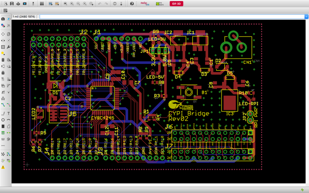
In the summer of 2013, I decided that I needed to design a printed circuit board.  I had worked on sections of chips but no PCBs.  I didnt really know which tool to use, but after looking around a bit it seemed like Eagle was a good simple choice as it had wide adoption in the Maker community.  At that point in time the Elkhorn Creek Measuring System was being run off a Raspberry PI and a PSoC5LP but Cypress had just released a new family of chips called the PSoC4200.  I thought that it would be a cool idea to have a PSoC to Raspberry PI bridge board.  So this is what I did.

On the bottom of the board I wanted female pins that matched the Raspberry PI, and on the top I wanted an Arduino pins.  Bottom line, I decided to build a board that was very similar to the CY8CKIT-042 except for having Raspberry PI GPIOs on the bottom of the board.

My board has:

  • Power System: Both 3.3v and 5.0v for the PSoC as well as 5.0v@1.0A for the Raspberry PI.
  • Reset System: A RPi connection to the PSoC and Arduino XRES.
  • An I2C connection between the RPi and the PSoC including the pullup resistors
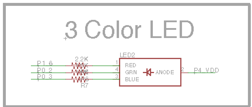
  • A 3-Color LED
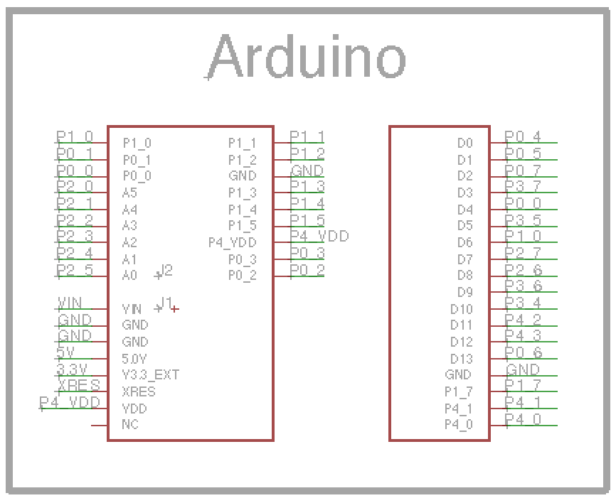
  • Arduino pins that match the pinout of the CY8CKIT-042

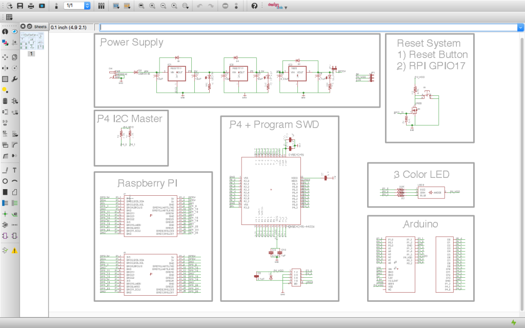
The overall schematic

Overall CYPI Schematic

I used the same RGB 3 Color LED (CLV1A-FKB- CJ1M1F1BB7R4S3) as exists on the CY8CKIT-042.

Screen Shot 2016-01-30 at 8.29.32 PM

I wanted to be able to reset PSoC and Arduino from the Raspberry Pi so I attached the RPi GPIO 1_11 to a pulldown transistor that is connected to the XRES of the Arduino and PSoC.  I also attached a small pushbutton to enable a user reset.

Screen Shot 2016-01-30 at 8.29.19 PM

I copied the Arduino pin out of the CY8CKIT-042.  This would allow me to easily use all of the projects that I had already developed that that development kit.

Screen Shot 2016-01-30 at 8.29.03 PM

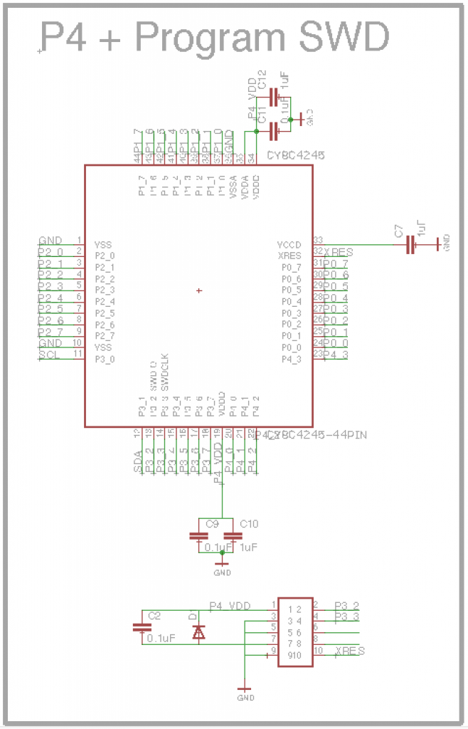
This section of the schematic has the required power supply decoupling capacitors.  It also has the ARM standard 10 Pin programming header which allows me to program the PSoC using a MiniProg-3.

Screen Shot 2016-01-30 at 8.28.46 PM

I provided pull up resistors on the PSoC P4[0] and P4[1] to easily enable the PSoC to serve as an I2C Master for the Arduino shield.

Screen Shot 2016-01-30 at 8.28.18 PM

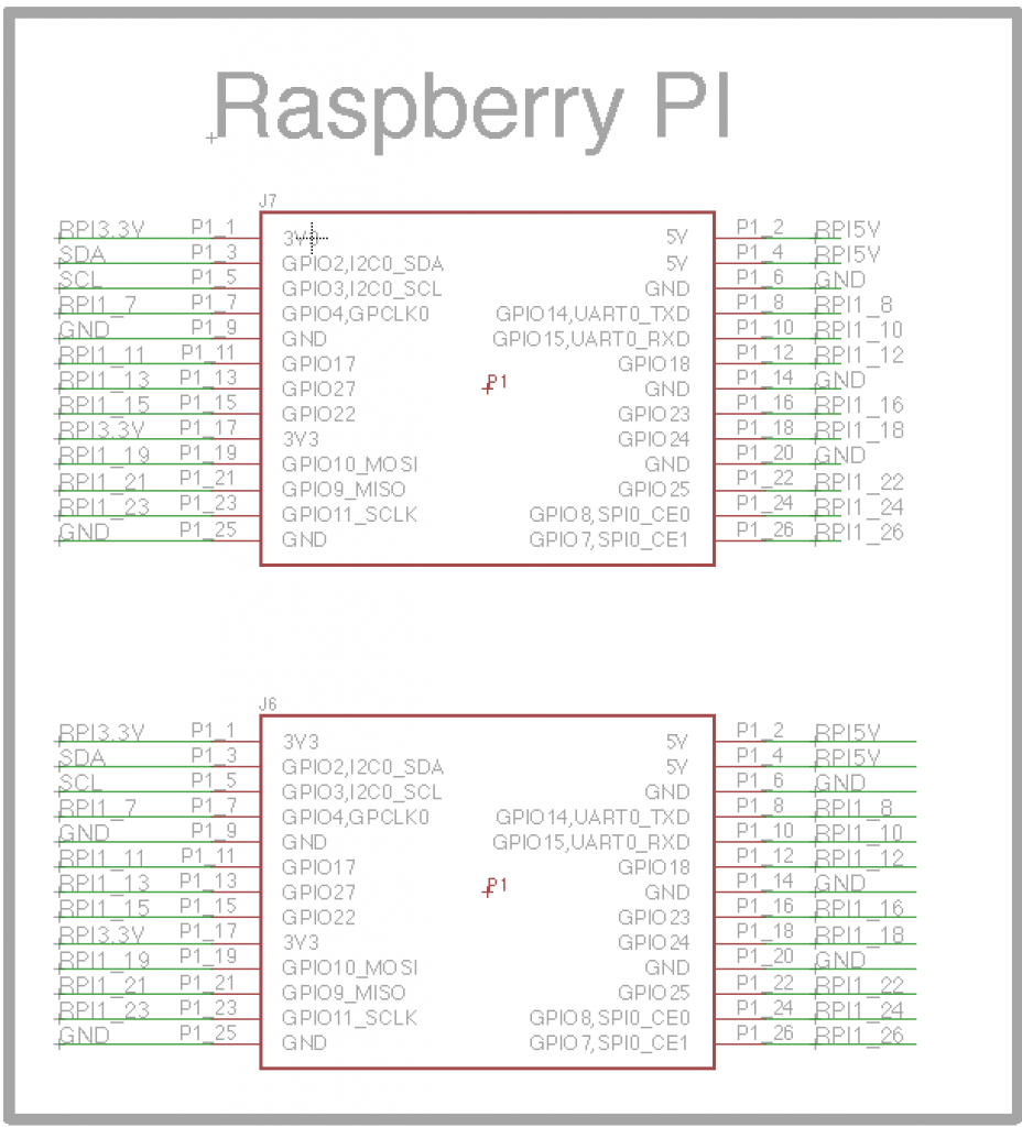
The connection to get data between the RPi and the PSoC is I2C.  The PSoC is setup as an I2C slave and the RPi is the master.  The connection on the RPi uses the RPI1_3 and RPI1_4 GPIOs.  On the PSoC it is connected to P3[0] and P3[1].

Screen Shot 2016-01-30 at 8.28.01 PM

The power supply turned out to be by far the most difficult part of the project.  In the first version of the board I chose a regulator that was to small to supply the Raspberry PI.  When the RPi was plugged in, the regulator immediately went into thermal shutdown.  In general this sucked as the PSoC Applications Manager warned me to pick a big enough regulator.  Oh well.  In the final version of the board I used a 7805 to supply the RPi, this regulator has a giant tab which allows you to sink heat into the ground plane of the board.  On the board I also provide a 5.0V supply and a 3.3V supply for the PSoC using a 1117 regulator.

Screen Shot 2016-01-30 at 8.27.34 PM

Here is a picture of the final layout

Overall Layout

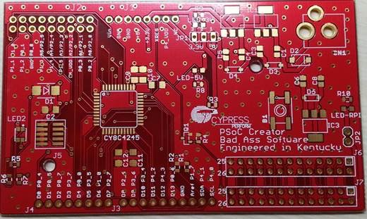
And here is a picture of the first version of the board.

IMG_1176 (1)

On thing that you might notice on this board is that the vias are exposed.  What I didnt know is that you need to tell Eagle to “tent” the vias so that they are covered with solder mask.

There is a lot going on in the layout and it is probably easiest to review the layout using eagle.  You can get the design from github at https://github.com/iotexpert/cypi

Index Description
The Creek: IOT for the Elkhorn Creek Introduction
The Creek: Solution Architecture 1.0 Overall architecture
The Creek: Creek Board 1.1 Eagle layout of the board
The Creek: Creek Board 1.0 – RCCA A discussion of the errors in the 1.0 board
The Creek: CYPI, a Raspberry Pi to Arduino Bridge PSoC4 <--> Raspberry Pi Bridge Board
The Creek: PSoC4 Creator Schematic and Firmware Firmware to interface with the temperature and pressure sensors
The Creek: Testing the Firmware Using tools to verify that the PSoC 4 Firmware is working correctly
The Creek: Testing the Bootloader Make sure that you can load new firmware into the PSoC
The Creek: Software Architecture All of the Raspberry Pi software connections
The Creek: Install MySql Instruction to configure MySql
The Creek: Install Tomcat Instruction to configure Tomcat JSP Server
The Creek: Data Collection Java (Part 1) The Java program that reads the I2C and saves it in the database
The Creek: Data Collection Java (Part 2) The Java program that reads the I2C and saves it in the database
The Creek: Create the Chart with JFreeChart Using open source Java charting software to create plots of the Creek Depth
The Creek: Flood Event Data Processor A batch program to create analyze the database and create a table of flood events
The Creek: Flood Event Web Page A batch program to create the flood event web page
The Creek: Creek Server 1.1 Updates to all of the back off server programs to integrate charts
The Creek: JSP Web Page for www.elkhorn-creek.org The JSP program to make the table and display the website
The Creek: Raspberry Pi Clock Stretching Sorting out a bug in the system having to do with the Broadcomm Raspberry Pi Master not functioning well with clock stretching
The Creek: Creek Server 1.2 Caching the web pages to make them faster

The Creek: Creek Board 1.0 – RCCA

At my company Cypress, “RCCA” is an abbreviation for “Root Cause Corrective Action”.  It is a formal process for changing the way that you work to prevent an error from happening again.

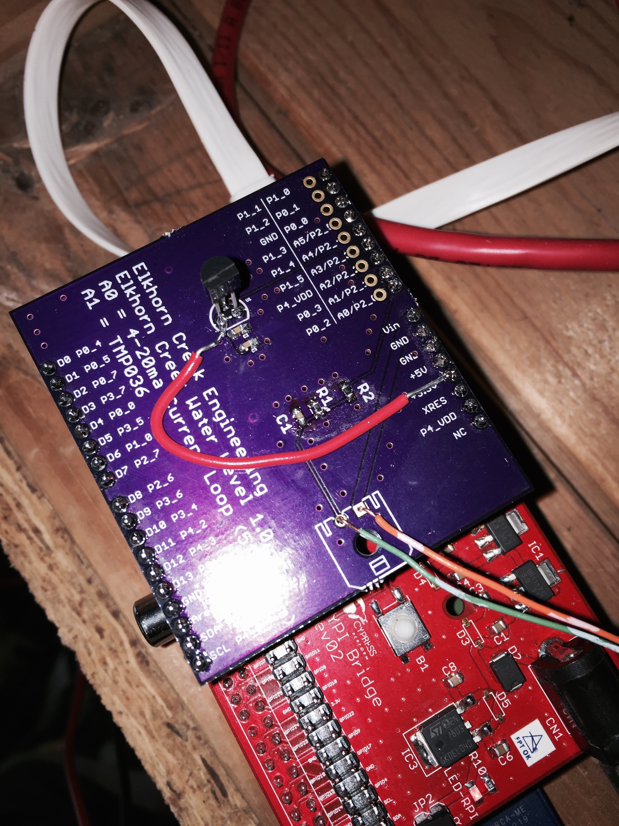
Unfortunately the title of this post is “Creek Board 1.0 – RCCA”.  What that means is that the first time I sent the Creek Board to be manufactured I made an error, in fact a really stupid error.  Specifically,  the error that I made was a fundamental failure of not having an LVS (Layout versus Schematic) clean design.  If you google “blue wire pcb” the first search result you will find is “Printed Circuit Board Repair and Rework Guides”,  I had no idea why blue wires were used to fix printed circuit boards so I called my friend Dave Van Ness.  He is an old grey beard type of guy.  He told me that the blue wire was traditionally an “official fix” to a circuit board.  It was used because other colors were already assigned (Red to power, Black to ground) etc.  I guess that I thumbed my nose at tradition by fixing my PCB with a red wire.

IMG_2024

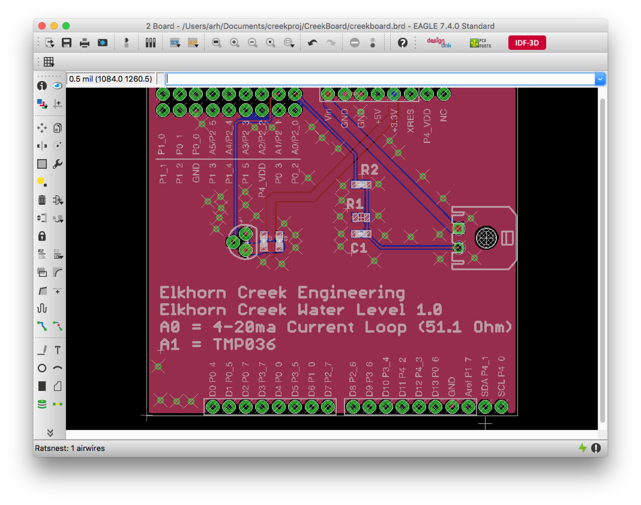
After laying out a printed circuit board, the last step is to surround the board with a ground plane on the top and bottom of the board.  Then you press the “ratsnest” button on Eagle.  Then Eagle does a “pour” which fills in the empty space of the board with a ground plane.  It then will update the bottom of the screen with the message “Ratsnet: Nothing to do!” which means all of the schematic and layout connections are complete.  Or, if there are connections that still need to be made, it will update the layout with yellow “air wires” and it will give you a message like “Ratsnest: 1 airwires.”  If you send the board to be made with an airwire, that is exactly what you will get.  I will tell you that air doesn’t conduct electricity very well and you will end up needing your soldering iron.

In this case I missed seeing the tiny little airwire.  See if you can see it:creek1.0board

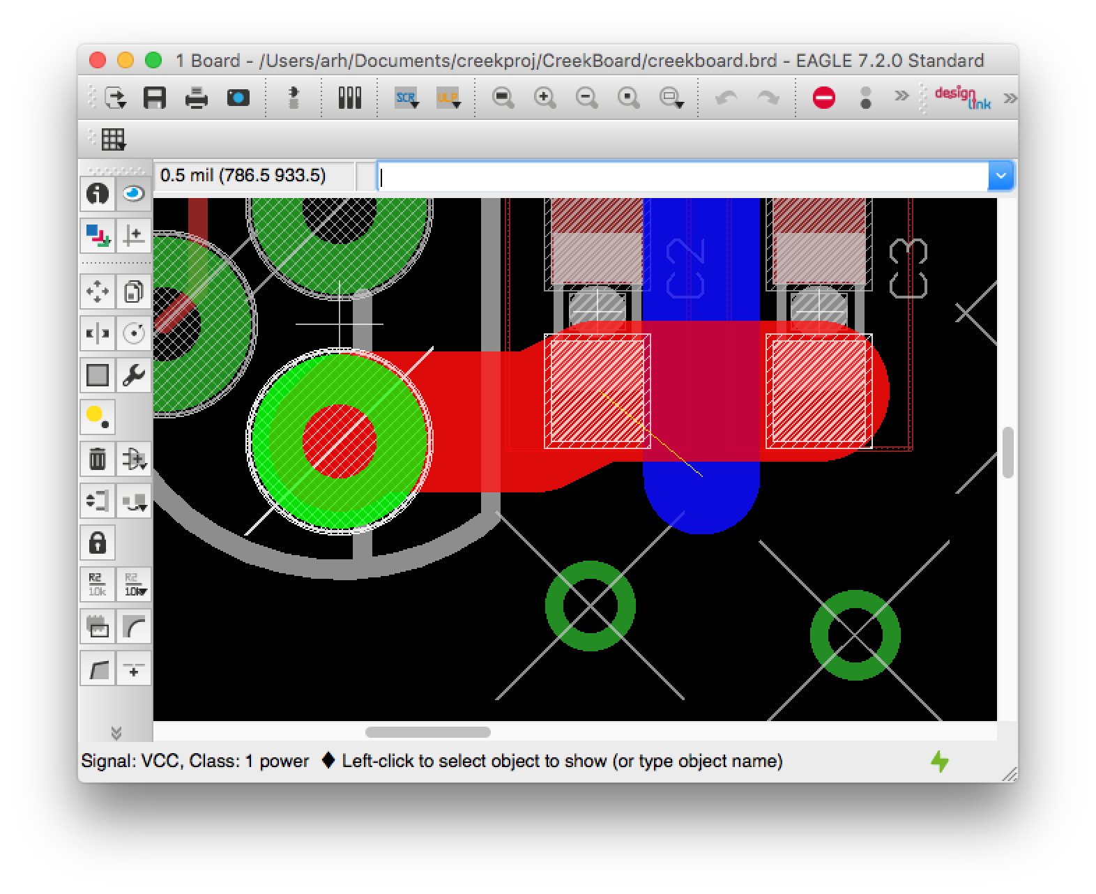
It is hard to see, eh?  In the next picture I turned off the ground layer and zoomed in so you can see that I am missing a power connection between the top and the bottom of the board.  I highlighted this issue by clicking on the “Show Objects” at the top of the toolbar, then clicking on yellow wire.  When I do that, Eagle tells me what the net is that is unconnected and it highlights every object that is attached to that net.

zoom-of-error

So now what?

What I ended up doing is the normal Cypress thing.  I created a “tapeout checklist”.  The checklist contains a list of all of the things that I double check before I send a PCB to be manufactured.  Here is my current (and short) checklist:

  • No remaining airwires
  • Vias tented (or not)
  • Silkscreen on all connections
  • Test points on key nets
  • No DRC errors

Index Description
The Creek: IOT for the Elkhorn Creek Introduction
The Creek: Solution Architecture 1.0 Overall architecture
The Creek: Creek Board 1.1 Eagle layout of the board
The Creek: Creek Board 1.0 – RCCA A discussion of the errors in the 1.0 board
The Creek: CYPI, a Raspberry Pi to Arduino Bridge PSoC4 <--> Raspberry Pi Bridge Board
The Creek: PSoC4 Creator Schematic and Firmware Firmware to interface with the temperature and pressure sensors
The Creek: Testing the Firmware Using tools to verify that the PSoC 4 Firmware is working correctly
The Creek: Testing the Bootloader Make sure that you can load new firmware into the PSoC
The Creek: Software Architecture All of the Raspberry Pi software connections
The Creek: Install MySql Instruction to configure MySql
The Creek: Install Tomcat Instruction to configure Tomcat JSP Server
The Creek: Data Collection Java (Part 1) The Java program that reads the I2C and saves it in the database
The Creek: Data Collection Java (Part 2) The Java program that reads the I2C and saves it in the database
The Creek: Create the Chart with JFreeChart Using open source Java charting software to create plots of the Creek Depth
The Creek: Flood Event Data Processor A batch program to create analyze the database and create a table of flood events
The Creek: Flood Event Web Page A batch program to create the flood event web page
The Creek: Creek Server 1.1 Updates to all of the back off server programs to integrate charts
The Creek: JSP Web Page for www.elkhorn-creek.org The JSP program to make the table and display the website
The Creek: Raspberry Pi Clock Stretching Sorting out a bug in the system having to do with the Broadcomm Raspberry Pi Master not functioning well with clock stretching
The Creek: Creek Server 1.2 Caching the web pages to make them faster

The Creek: Creek Board 1.1

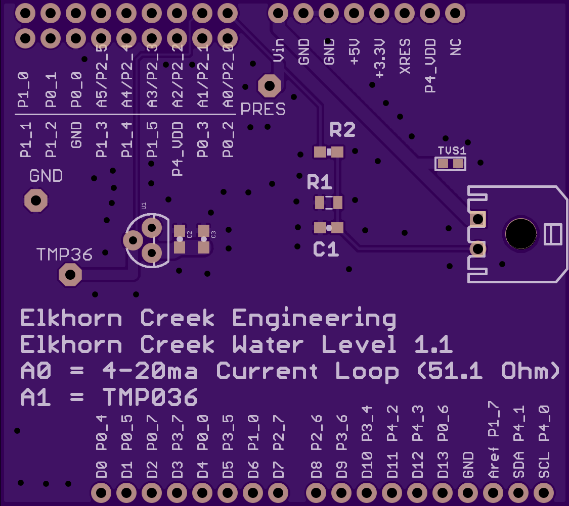
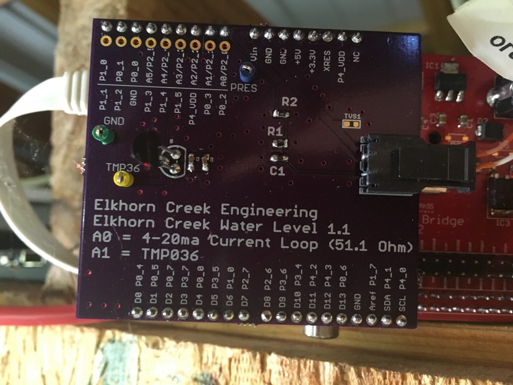
In the previous post I described the entire system architecture.  In this post, I am going to describe the Arduino shield that I unfortunately call “Elkhorn Creek Water Level 1.1”.  It is unfortunate because in version 1.0 I made a really stupid error which ruined the first run of printed circuit boards.  You can read more about how I made the error and what I am doing in the future in the post Creek Board 1.0 RCCA.

To make this system work I need to be able to interface the PSoC4200 with two sensors:

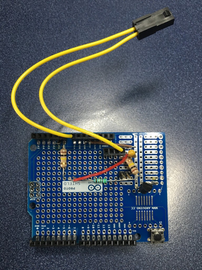
Both of these sensors are subject to environmental noise so they both have capacitive or RC filters connected to them.  I originally built a prototype of this board using a proto board.  However, it was a PITA because the wires would come loose and the system would stop working.

IMG_2655

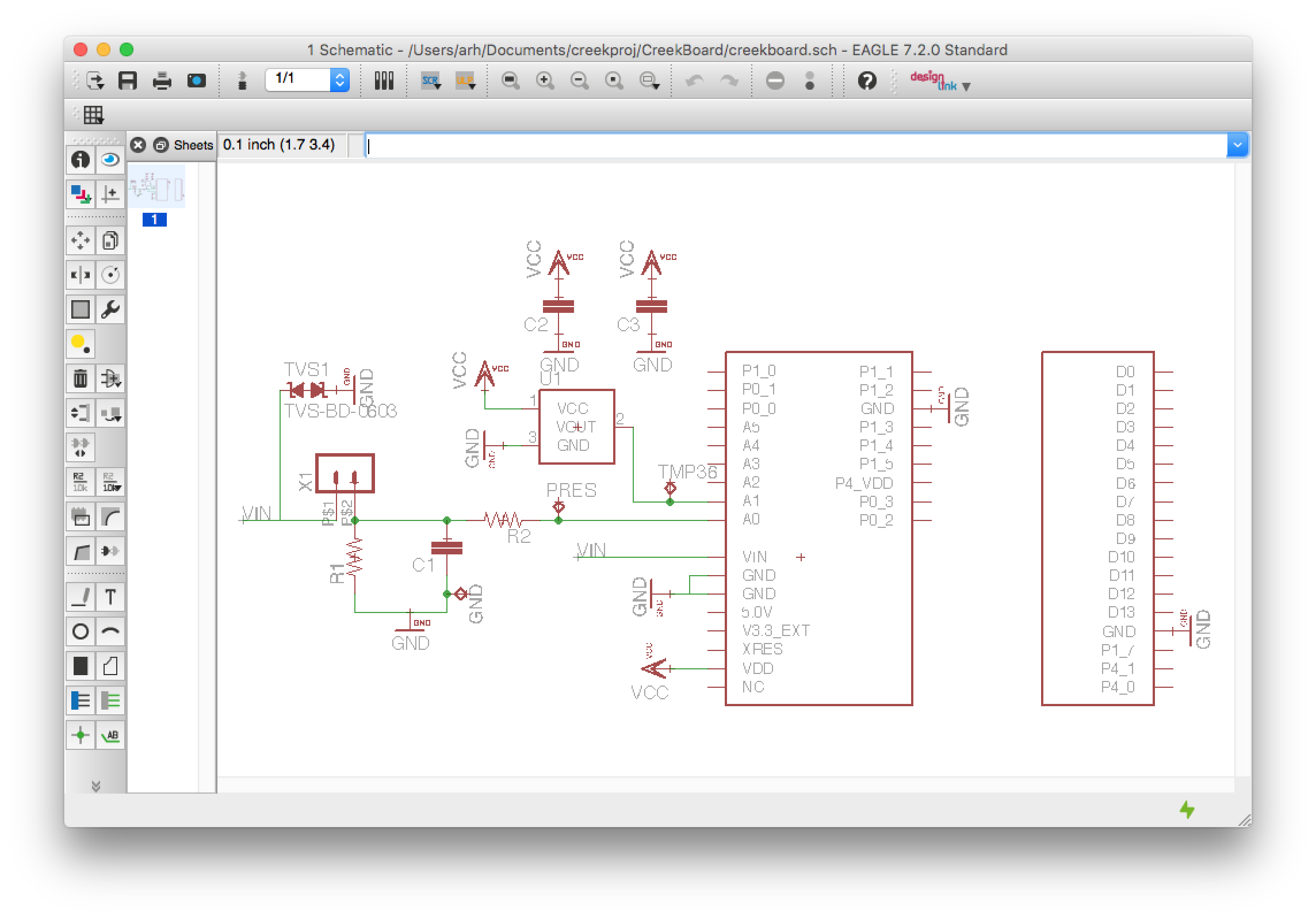
So I decided to make a real PCB.  To do the design, I used the Eagle 7.2 PCB editor as it seemed like it had the most support from the maker community.  The schematic for the system is fairly simple.  It has

  • Pressure Sensor
    • X1: A Molex Microfit 3.0 Connector to attach the two wires from the pressure sensor
    • R1: A 51.1 Ohm resistor to group to convert the 4-20mA –>  0.204mV to 1.022V
    • C1/R2: A low pass filter
    • TVS1: A ESD diode to clamp any ESD event to ground to prevent it from blowing up the PSoC4A or the Sensor
  • Temperature Sensor
    • TMP36: A sensor that turns temperature into a voltage.  The equation for temperature is T=0.5V+10mV/degreeC.  For 25 degrees C the Voltage = 750mV
    • C2 + C3: Two decoupling capacitors to filter power supply noise
  • Arduino Interface
    • A standard Arduino interface set of pins + the additional Cypress CY8CKIT-042 pins.  I only used the A0 and A1 pins for signals and the Vin pin (which is 12v) to drive the current loop
  • Measurement Test Points
    • Keystone 5000 test points.  These test points are a little loop of wire that sticks up from the surface of the PCB to make  it easy to probe a voltage with your DMM.  5000_sml

Here is the final Eagle Schematic for the board.

CreekBoardSchematic

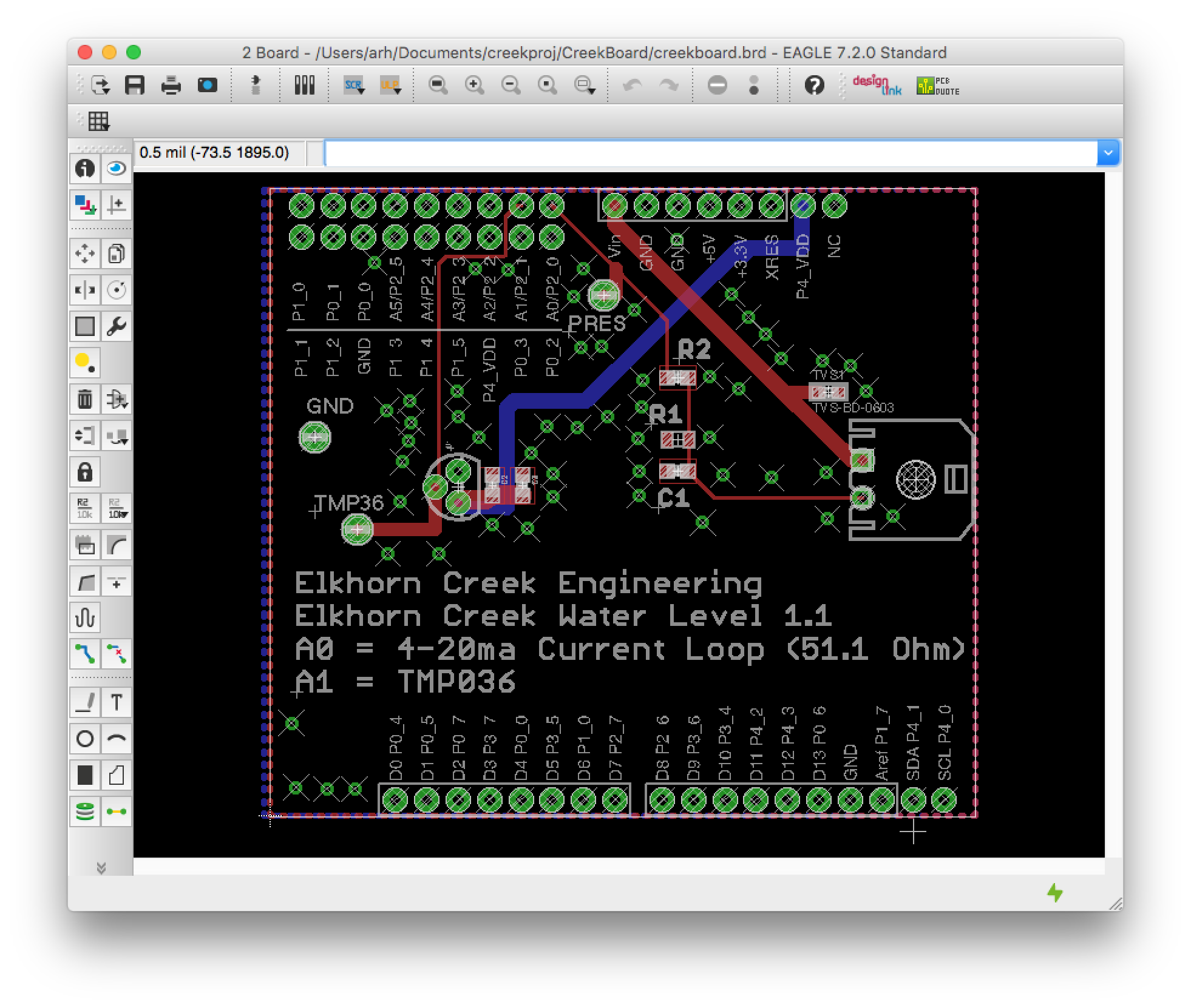
And the layout:CreekBoard2.0Layout

Once I completed the layout I sent the board to OSH Park to be manufactured.  I have shared the project on their website.  OSH Park is an excellent company that is easy to do business with.  They charged me $22.55 for three of the boards.  The fit and finish of the boards is very nice.  Here is the board:

creekboard1.1

Here is the assembled board:


IMG_2652

I have posted all of the project files at github.  You can “git” them from https://github.com/iotexpert/TheCreek  The Eagle project is in the CreekBoard directory.

Index Description
The Creek: IOT for the Elkhorn Creek Introduction
The Creek: Solution Architecture 1.0 Overall architecture
The Creek: Creek Board 1.1 Eagle layout of the board
The Creek: Creek Board 1.0 – RCCA A discussion of the errors in the 1.0 board
The Creek: CYPI, a Raspberry Pi to Arduino Bridge PSoC4 <--> Raspberry Pi Bridge Board
The Creek: PSoC4 Creator Schematic and Firmware Firmware to interface with the temperature and pressure sensors
The Creek: Testing the Firmware Using tools to verify that the PSoC 4 Firmware is working correctly
The Creek: Testing the Bootloader Make sure that you can load new firmware into the PSoC
The Creek: Software Architecture All of the Raspberry Pi software connections
The Creek: Install MySql Instruction to configure MySql
The Creek: Install Tomcat Instruction to configure Tomcat JSP Server
The Creek: Data Collection Java (Part 1) The Java program that reads the I2C and saves it in the database
The Creek: Data Collection Java (Part 2) The Java program that reads the I2C and saves it in the database
The Creek: Create the Chart with JFreeChart Using open source Java charting software to create plots of the Creek Depth
The Creek: Flood Event Data Processor A batch program to create analyze the database and create a table of flood events
The Creek: Flood Event Web Page A batch program to create the flood event web page
The Creek: Creek Server 1.1 Updates to all of the back off server programs to integrate charts
The Creek: JSP Web Page for www.elkhorn-creek.org The JSP program to make the table and display the website
The Creek: Raspberry Pi Clock Stretching Sorting out a bug in the system having to do with the Broadcomm Raspberry Pi Master not functioning well with clock stretching
The Creek: Creek Server 1.2 Caching the web pages to make them faster