Summary
In this article I build several different programs to measure the DeepSleep to Active wakeup time of the PSoC 6 which ranges from 15uS to 120uS. I will discuss the data sheet max of 25uS and the useful limit of about 60uS. I will include an analysis of the system issues that will influence your wakeup time.
This article is part of the "PSoC 6 Low Power Techniques" Series which covers a range of tools you have to lower the power of your system. The following articles are (or will be) available:
Articles
PSoC 6 Low Power
PSoC 6 & Using the MCWDT as a Deep Sleep Timer
PSoC 6 Deep Sleep Wakeup Time
PSoC 6 & FreeRTOS Tickless
Managing the PSoC 6 Clock Frequency
Using the PSoC 6 LDO and SIMO Buck Regulators for Low Power
Using the PSoC 6 Always on Backup Domain
PSoC 6 Turning off block of RAM
The following resources are available
| Resource |
|---|
| Cypress Application Note: PSoC 6 MCU Low-Power Modes and Power Reduction Techniques |
The Story
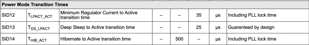
As I was working on implementing the FreeRTOS tickless mode I noticed (incorrectly) that the wakeup time from DeepSleep was around 5ms. When I saw this number I thought “wow, that is a long time”, then I looked at the data sheet and discovered that it was really “25 uS Guaranteed by design”. Given that Cypress is very careful about our data sheet numbers I thought “wow… 25uS is a long way from 5ms. Did we really make that bad an error in the data sheet?”
I decided to dig in to figure out what was really happening. The real answer is that the wakeup time isn’t anywhere near 5ms. That turned out to be an IoT Expert Alan bug (shhhh don’t tell anyone), but it did turn into an interesting investigation of the PSoC 6 chip.
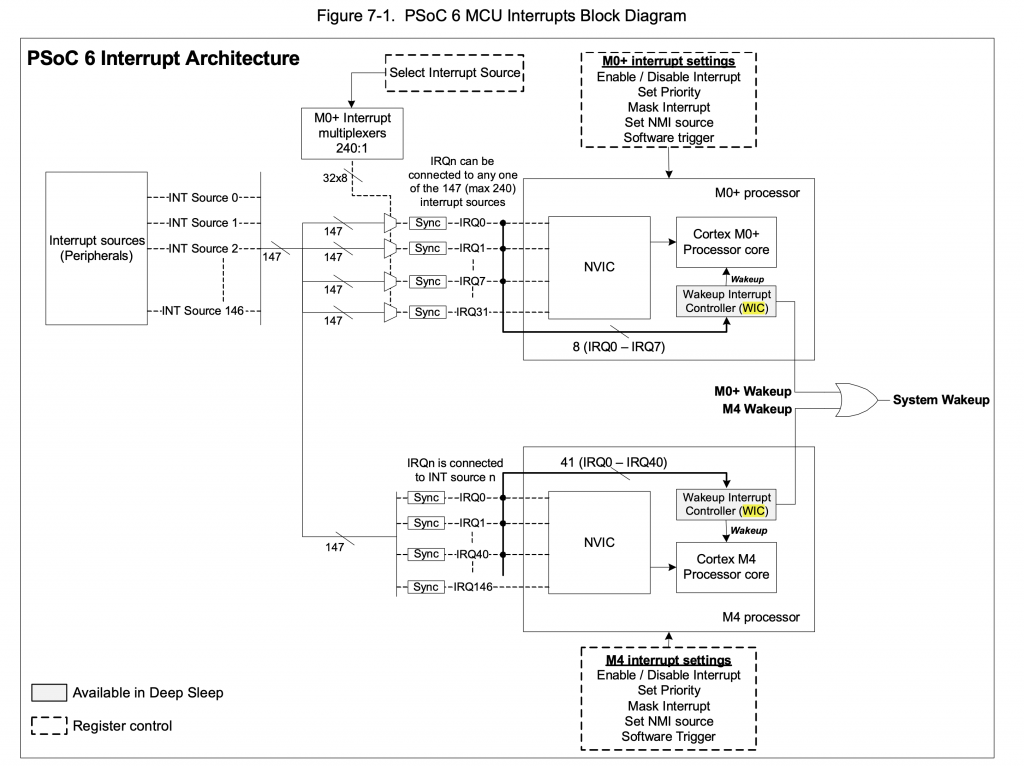
In order to measure the wakeup time I needed a way to measure between a wakeup trigger and the system being awake. The best way seemed to use a pin to trigger the wakeup and pin to indicate the system being awake. Then measure using an oscilloscope. In the PSoC 6, in order to wakeup the system you need to send an interrupt to the Wakeup Interrupt Controller, here is a picture from the TRM. These interrupts also serve as interrupts for the ARM Cores.
The basic flow of all of these examples is:
- Enable interrupts on the input pin which is attached to SW2 aka P04 or Arduino D0
- Write a 0 to the P50/D0 output pin
- DeepSleep
- Write a 1 to the P50/D0 output pin
- Go back to 2
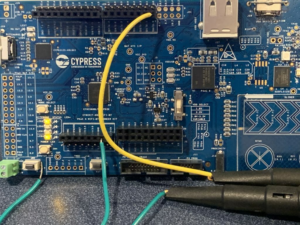
Here is a picture of my CY8CKIT-062-WiFi-BT development kit. Notice that I soldered a wire to the Switch (SW2) which is connected to P04. The green switch wire is barely attached because I didn’t want to delaminate the switch from the board. The yellow wire is attached to P50/D0.
What follows is a discussion of 7 different configurations. As much as possible I try to use the Cypress Hardware Abstraction Layer (HAL) but as I dig, I get down to writing registers directly.
- Basic Pin Event and HAL Write
- Register Custom ISR Instead of HAL ISR
- Disable ARM Interrupts (no ISR)
- Write the Output Pin Register Directly (no HAL)
- Try Different Clock Frequencies
- Modify the Cypress PDL Function Cy_SysPm_EnterDeepSleep
- Write the ARM DeepSleep Register Directly and Call __WIFI
Basic Pin Event and HAL Write
I started with this very simple example. The steps are:
- Use the HAL to enable two output pins (one attached to the LED) and one attached to the Oscilliscope.
- Use the HAL to configure the Switch as an input and then enable interrupts on that switch.
Go into the main loop and:
- Write the LED to On (aka 0) to indicate DeepSleep
- Write the D0 to 0
- DeepSleep
- Write the D0 to 1
- Write the LED to Off (to indicate Active)
- Do a little delay… then do it all over again
int main(void)
{
    /* Initialize the device and board peripherals */
    cybsp_init();

    cyhal_gpio_init(CYBSP_D0,CYHAL_GPIO_DIR_OUTPUT,CYHAL_GPIO_DRIVE_STRONG,0);
    cyhal_gpio_init(CYBSP_SW2,CYHAL_GPIO_DIR_INPUT,CYHAL_GPIO_DRIVE_PULLUP,1);
    cyhal_gpio_init(CYBSP_USER_LED,CYHAL_GPIO_DIR_OUTPUT,CYHAL_GPIO_DRIVE_STRONG,1);

    cyhal_gpio_enable_event(CYBSP_SW2, CYHAL_GPIO_IRQ_FALL, 4, true);

	__enable_irq();

    while(1)
    {
    	cyhal_gpio_write(CYBSP_USER_LED,0);
    	cyhal_gpio_write(CYBSP_D0,0);
    	cyhal_system_deepsleep();
    	cyhal_gpio_write(CYBSP_D0,1);
    	cyhal_gpio_write(CYBSP_USER_LED,1);
    	CyDelay(2000);
    }
}
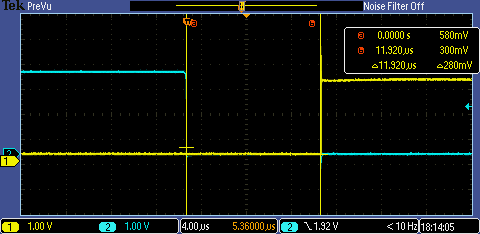
When I measure this on the Oscilloscope I get 57uS

Register Custom ISR Instead of HAL ISR
Well, 57uS is definitely more than 25uS (though it is way way less than 5ms). I wondered why isn’t it meeting spec. And I thought, maybe it is burning time in the HAL pin interrupt service routine. So, I decided to attach my own ISR.
First there is an interrupt service routine function called “buttonHandler” which toggles the D0 pin to 1, then clears the port interrupt.
In the main function instead of enabling the event, I setup the interrupt directly by:
- Configuring the Port for interrupts
- Setting the edge to falling (because there is a resistive pullup on the switch)
- Loading my own ISR
- Enabling the interrupt
Then in the main loop I remove the D0 pin write to 1.
#include "cybsp.h"
#include "cyhal.h"
#include "cycfg.h"

void buttonHandler()
{
	cyhal_gpio_write(CYBSP_D0,1);
	Cy_GPIO_ClearInterrupt(GPIO_PRT0,4);
}


int main(void)
{
    /* Initialize the device and board peripherals */
    cybsp_init();


    cyhal_gpio_init(CYBSP_D0,CYHAL_GPIO_DIR_OUTPUT,CYHAL_GPIO_DRIVE_STRONG,0);
    cyhal_gpio_init(CYBSP_SW2,CYHAL_GPIO_DIR_INPUT,CYHAL_GPIO_DRIVE_PULLUP,1);
    cyhal_gpio_init(CYBSP_USER_LED,CYHAL_GPIO_DIR_OUTPUT,CYHAL_GPIO_DRIVE_STRONG,1);


	Cy_GPIO_SetInterruptMask(GPIO_PRT0,4,1);
	Cy_GPIO_SetInterruptEdge(GPIO_PRT0,4,CY_GPIO_INTR_FALLING);

	Cy_SysInt_SetVector(ioss_interrupts_gpio_0_IRQn, buttonHandler);

	NVIC_EnableIRQ(ioss_interrupts_gpio_0_IRQn);

    __enable_irq();

    while(1)
    {
    	cyhal_gpio_write(CYBSP_USER_LED,0);
    	cyhal_gpio_write(CYBSP_D0,0);
    	cyhal_system_deepsleep();
    	cyhal_gpio_write(CYBSP_USER_LED,1);
    	CyDelay(2000);
    }
}
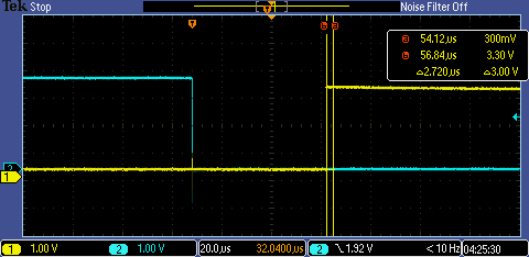
When I measure this, I find that it is 54uS instead of 57uS (notice I left the cursors from the previous measurement)
Disable ARM Interrupts (no ISR)
Then I think maybe the problem is the jump to the ISR. Inside the ARM there are two enable controls over interrupts
- In the NVIC
- A global ARM interrupt control
So, I use the cyhal_gpio_enable_event to enable the NVIC. Then I use the CMSIS function __disable_irq to turn off the ARM interrupts.
int main(void)
{
    /* Initialize the device and board peripherals */
    cybsp_init();

    cyhal_gpio_init(CYBSP_D0,CYHAL_GPIO_DIR_OUTPUT,CYHAL_GPIO_DRIVE_STRONG,0);
    cyhal_gpio_init(CYBSP_SW2,CYHAL_GPIO_DIR_INPUT,CYHAL_GPIO_DRIVE_PULLUP,1);
    cyhal_gpio_init(CYBSP_USER_LED,CYHAL_GPIO_DIR_OUTPUT,CYHAL_GPIO_DRIVE_STRONG,1);

    cyhal_gpio_enable_event(CYBSP_SW2, CYHAL_GPIO_IRQ_FALL, 4, true);

	__disable_irq();

    while(1)
    {
    	cyhal_gpio_write(CYBSP_USER_LED,0);
    	cyhal_gpio_write(CYBSP_D0,0);
    	cyhal_system_deepsleep();
    	cyhal_gpio_write(CYBSP_D0,1);
    	cyhal_gpio_write(CYBSP_USER_LED,1);
    	CyDelay(2000);
    }
}
Now it is 53uS or basically the same as before. So this doesn’t explain the missing 30uS (or whatever is required to get blow the data sheet spec)
Write the Output Pin Register Directly (no HAL)
Then I think to myself, maybe the HAL functions are slow. Look at the pin write function:
cyhal_gpio_write(CYBSP_D0,0);
When you look at the function you see that it is really a MACRO for an inline call to the PDL function
__STATIC_INLINE void cyhal_gpio_write_internal(cyhal_gpio_t pin, bool value)
{
    Cy_GPIO_Write(CYHAL_GET_PORTADDR(pin), CYHAL_GET_PIN(pin), value);
}

#define cyhal_gpio_write(pin, value) cyhal_gpio_write_internal(pin, value)
The inline PDL function turns a pin number into a Port, Pin combination with a call to some other PDL functions.
#define CYHAL_GET_PORTADDR(pin) (Cy_GPIO_PortToAddr(CYHAL_GET_PORT(pin))) /**< Macro to get the port address from pin */
Those functions basically lookup the bit mask and base address of the Port,Pin. Plus they have some error checking.
__STATIC_INLINE GPIO_PRT_Type* Cy_GPIO_PortToAddr(uint32_t portNum)
{
    GPIO_PRT_Type* portBase;

    if(portNum < (uint32_t)IOSS_GPIO_GPIO_PORT_NR)
    {
        portBase = (GPIO_PRT_Type *)(CY_GPIO_BASE + (GPIO_PRT_SECTION_SIZE * portNum));
    }
    else
    {
        /* Error: Return default base address */
        portBase = (GPIO_PRT_Type *)(CY_GPIO_BASE);
    }

    return (portBase);
}
Then they call this macro:
GPIO_PRT_OUT_SET(GPIO_PRT5) = 0x01;
Which is just a direct register write.
(((GPIO_PRT_V1_Type*)(base))->OUT_SET)
So I change over my program to write directly to the port register and is make ZERO difference. On the range where I can see the pulse between the interrupt and the pin write, the difference is too small to register.
Try Different Clock Frequencies
The next thing that I wonder is if the CPU frequency matters. On my board there are three possible sources of CM4 clock.
- The 8MHz IMO
- The FLL (also known as CLK_PATH0)
- The PLL (also known as CLK_PATH1)
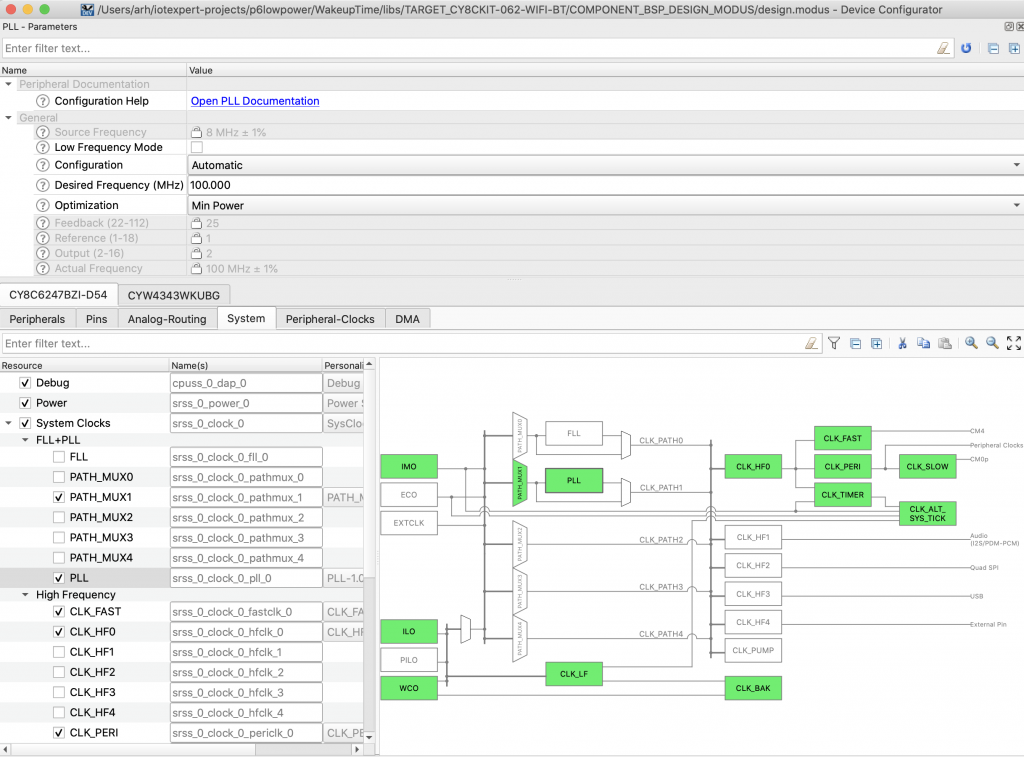
To try the different possibilities, I start by selecting CLK_PATH1 (the PLL) as the source clock for CLK_HF0
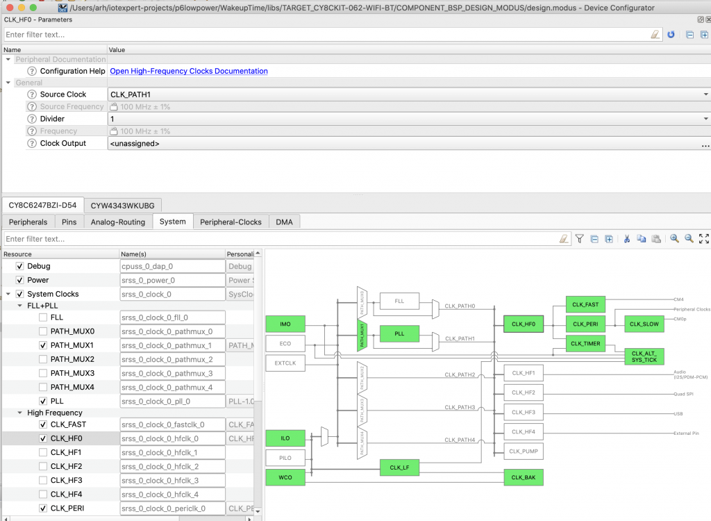
Then configure the PLL to 100 MHz
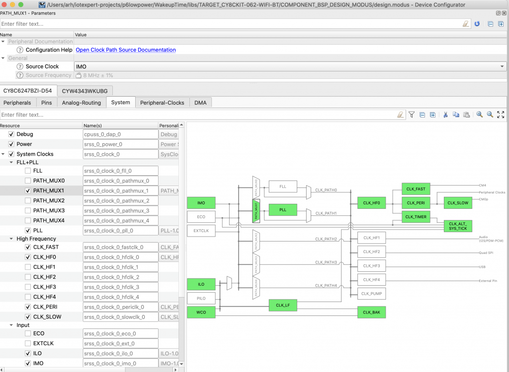
Then I tell the “PATH_MUX1” to use the IMO
Then I start running tests. Here is the table of results for a bunch of different combinations.
| Freq | PLL | FLL | IMO |
|---|---|---|---|
| 8 MHz | - | - | 119 uS |
| 12.5 MHz | 102 uS | - | - |
| 25 MHz | 73uS | 102 uS | - |
| 50 MHz | 60uS | 102 uS | - |
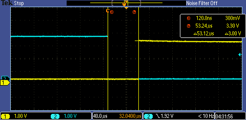
| 100 MHz | 53uS | 102 uS | - |
| 150 MHz | 53 uS | - | - |
OK. The “wakeup” time seems to depend on the clock source and frequency. First, notice that if you use the PLL that it typically takes 16uS to lock … and it could take as much as 35uS. That explains part of the difference.

The FLL consistently takes 7.uS to lock. In fact that is the main reason it exists on this chip.

We know that the FLL and PLL explain some of the difference in the startup time. But where is the rest?
Modify the Cypress PDL Function Cy_SysPm_EnterDeepSleep
The answer is that there are a bunch of things that happen AFTER the chip wakes up inside of the Cy_SysPm_EnterDeepSleep. These things are part of the house keeping that it takes to make everything really work.
First, look at the cyhal_system_deepsleep() function, which is really just a #define for the PDL DeepSleep function.
#define cyhal_system_deepsleep() Cy_SysPm_CpuEnterDeepSleep(CY_SYSPM_WAIT_FOR_INTERRUPT)
If you dig through that function you will find yourself down in another function named “EnterDeepSleepRam. If you look on line 2965 you will find that the code sets the bit in the ARM System Control Register which tells it to DeepSleep. Then on line 2969 it executes the ARM assembly language instruction “WFI” also known as Wait For interrupt. The WFI puts the CPU to sleep, or deep sleep depending on bit in the SCR register. On lines 2970, 2993 and 3030 you can see that I instrumented the code to toggle the D0 GPIO so I can measure time.
/*******************************************************************************
* Function Name: EnterDeepSleepRam
****************************************************************************//**
*
* The internal function that prepares the system for Deep Sleep and
* restores the system after a wakeup from Deep Sleep.
*
* \param waitFor
* Selects wait for action. See \ref cy_en_syspm_waitfor_t.
*
* \return
* - true - System Deep Sleep was occurred.
* - false - System Deep Sleep was not occurred.
*
*******************************************************************************/
#if defined (__ICCARM__)
    #pragma diag_suppress=Ta023
    __ramfunc
#else
    CY_SECTION(".cy_ramfunc") CY_NOINLINE
#endif
static void EnterDeepSleepRam(cy_en_syspm_waitfor_t waitFor)
{
    /* Store the address of the Deep Sleep indicator into the RAM */
    volatile uint32_t *delayDoneFlag = &FLASHC_BIST_DATA_0;

#if (CY_CPU_CORTEX_M4)

    /* Store the address of the CM4 power status register */
    volatile uint32_t *cpussCm4PwrCtlAddr = &CPUSS_CM4_PWR_CTL;

    /* Repeat the WFI/WFE instruction if a wake up was not intended.
    *  Cypress ID #272909
    */
    do
    {
#endif /* (CY_CPU_CORTEX_M4) */

        /* The CPU enters Deep Sleep mode upon execution of WFI/WFE */
        SCB_SCR |= SCB_SCR_SLEEPDEEP_Msk;

        if(waitFor != CY_SYSPM_WAIT_FOR_EVENT)
        {
            __WFI();
        	GPIO_PRT_OUT_SET(GPIO_PRT5) = 0x01;

        }
        else
        {
            __WFE();

        #if (CY_CPU_CORTEX_M4)
            /* Call the WFE instruction twice to clear the Event register
            *  of the CM4 CPU. Cypress ID #279077
            */
            if(wasEventSent)
            {
                __WFE();
            }
            wasEventSent = true;
        #endif /* (CY_CPU_CORTEX_M4) */
        }

#if (CY_CPU_CORTEX_M4)
    } while (_FLD2VAL(CPUSS_CM4_PWR_CTL_PWR_MODE, (*cpussCm4PwrCtlAddr)) == CM4_PWR_STS_RETAINED);
#endif /* (CY_CPU_CORTEX_M4) */

	GPIO_PRT_OUT_CLR(GPIO_PRT5) = 0x01;

    /* Set 10 uS delay only under condition that the FLASHC_BIST_DATA[0] is
    *  cleared. Cypress ID #288510
    */
    if (*delayDoneFlag == NEED_DELAY)
    {
        uint32_t ddftSlowCtl;
        uint32_t clkOutputSlow;
        uint32_t ddftFastCtl;

        /* Save timer configuration */
        ddftSlowCtl   = SRSS_TST_DDFT_SLOW_CTL_REG;
        clkOutputSlow = SRSS_CLK_OUTPUT_SLOW;
        ddftFastCtl   = SRSS_TST_DDFT_FAST_CTL_REG;

        /* Configure the counter to be sourced by IMO */
        SRSS_TST_DDFT_SLOW_CTL_REG = SRSS_TST_DDFT_SLOW_CTL_MASK;
        SRSS_CLK_OUTPUT_SLOW       = CLK_OUTPUT_SLOW_MASK;
        SRSS_TST_DDFT_FAST_CTL_REG = TST_DDFT_FAST_CTL_MASK;

        /* Load the down-counter to count the 10 us */
        SRSS_CLK_CAL_CNT1 = IMO_10US_DELAY;

        while (0U == (SRSS_CLK_CAL_CNT1 & SRSS_CLK_CAL_CNT1_CAL_COUNTER_DONE_Msk))
        {
            /* Wait until the counter stops counting */
        }

        /* Indicate that delay was done */
        *delayDoneFlag = DELAY_DONE;

        /* Restore timer configuration */
        SRSS_TST_DDFT_SLOW_CTL_REG = ddftSlowCtl;
        SRSS_CLK_OUTPUT_SLOW       = clkOutputSlow;
        SRSS_TST_DDFT_FAST_CTL_REG = ddftFastCtl;
    }
	GPIO_PRT_OUT_SET(GPIO_PRT5) = 0x01;


}
#if defined (__ICCARM__)
Here is the SCR register documentation where you can see the bit “SLEEPDEEP” bit[2]
And later in the documentation the Wait For Interrupt (WFI) instruction.
When I ran the code I got:
- From the falling edge of the to the rising edge is 17.12uS (deep sleep to first instruction on line 2970)
- From the rising to falling edge is 6.25uS (line 2970 to line 2993)
- From the falling to riding edge is 30uS (line 2993 to 3030)
- From the rising to falling edge is 3.5uS (line 3030 to the first line in the main function)
Here is the scope trace.
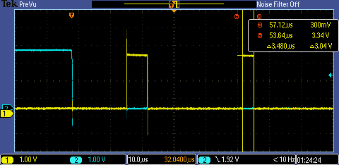
What does it all mean? There are basically three things going on from the Wakeup until the application developer has control.
- Cypress implementation of work arounds for chip issues
- Synchronization between the two MCUs in the PSoC 6
- Unwinding the DeepSleep preparations (user callbacks)
Write the ARM DeepSleep Register Directly and Call __WIFI
So this gives us a hint. We could implement just the DeepSleep instructions. If you did, the code would look like this:
#include "cybsp.h"
#include "cyhal.h"
#include "cycfg.h"


int main(void)
{
    /* Initialize the device and board peripherals */
    cybsp_init();

    cyhal_gpio_init(CYBSP_D0,CYHAL_GPIO_DIR_OUTPUT,CYHAL_GPIO_DRIVE_STRONG,0);
    cyhal_gpio_init(CYBSP_SW2,CYHAL_GPIO_DIR_INPUT,CYHAL_GPIO_DRIVE_PULLUP,1);
    cyhal_gpio_init(CYBSP_USER_LED,CYHAL_GPIO_DIR_OUTPUT,CYHAL_GPIO_DRIVE_STRONG,1);

    cyhal_gpio_enable_event(CYBSP_SW2, CYHAL_GPIO_IRQ_FALL, 4, true);


    __disable_irq();

    while(1)
    {
    	cyhal_gpio_write(CYBSP_D0,0);

        SCB_SCR |= SCB_SCR_SLEEPDEEP_Msk;
        __WFI();
    	GPIO_PRT_OUT_SET(GPIO_PRT5) = 0x01;

    	Cy_GPIO_ClearInterrupt(GPIO_PRT0,4);
    	NVIC_ClearPendingIRQ	(	ioss_interrupts_gpio_0_IRQn	)	;
    	cyhal_gpio_write(CYBSP_USER_LED,0);

    	CyDelay(2000);
    	cyhal_gpio_write(CYBSP_USER_LED,1);

    }
}
Well there it is 12uS. That is for sure below the data sheet limit of 25uS.
But is it a good idea? No, almost certainly not. If you don’t call the Cypress functions you will
- Not be protected from the dual core interactions
- Not call our functions to work around silicon bugs
- Potentially not manage the clocks correctly
So unless you have some really compelling reason you should just use the Cypress functions and accept the 50ish uS to get back to Active.
No comment yet, add your voice below!