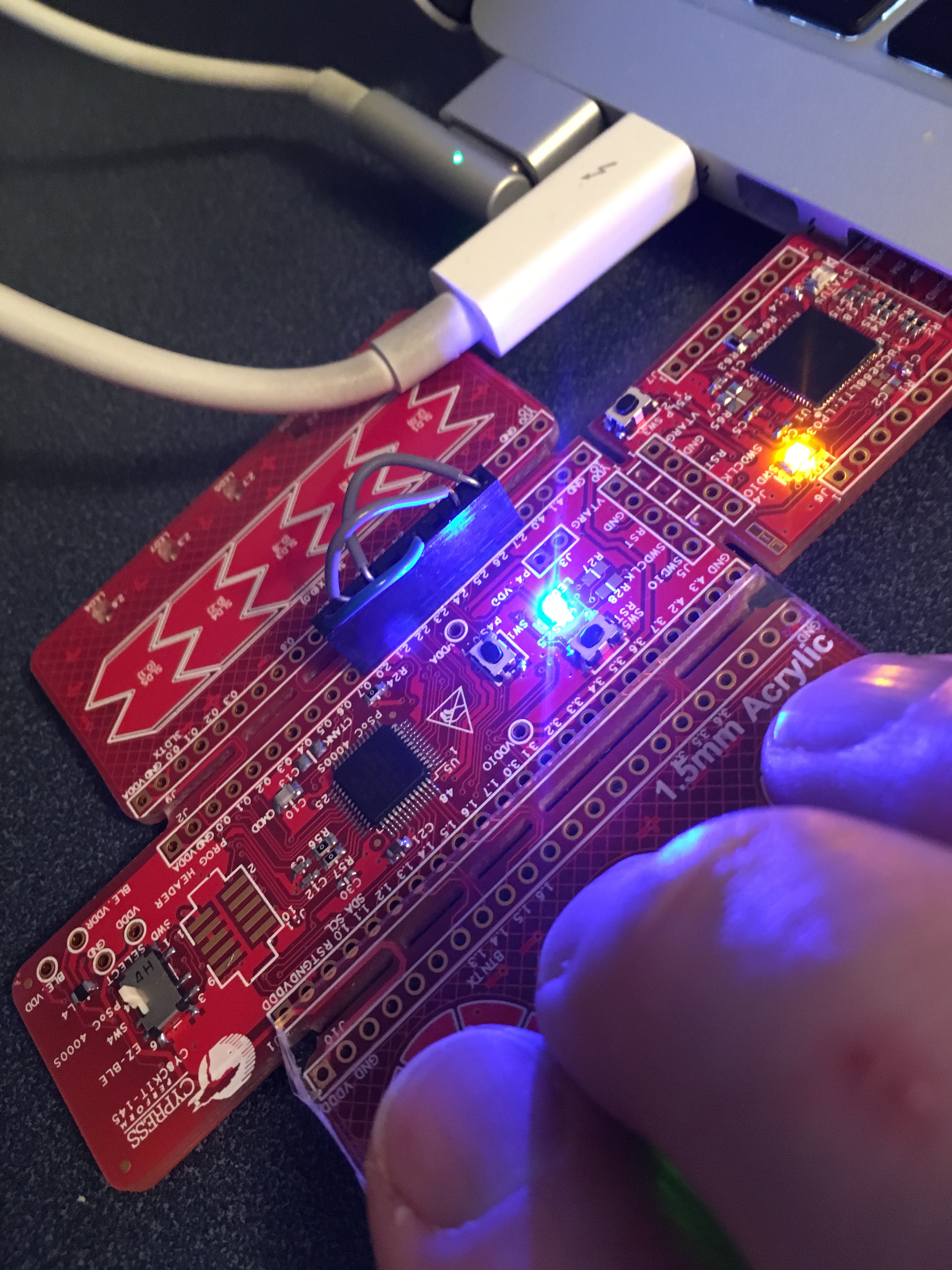
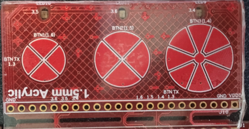
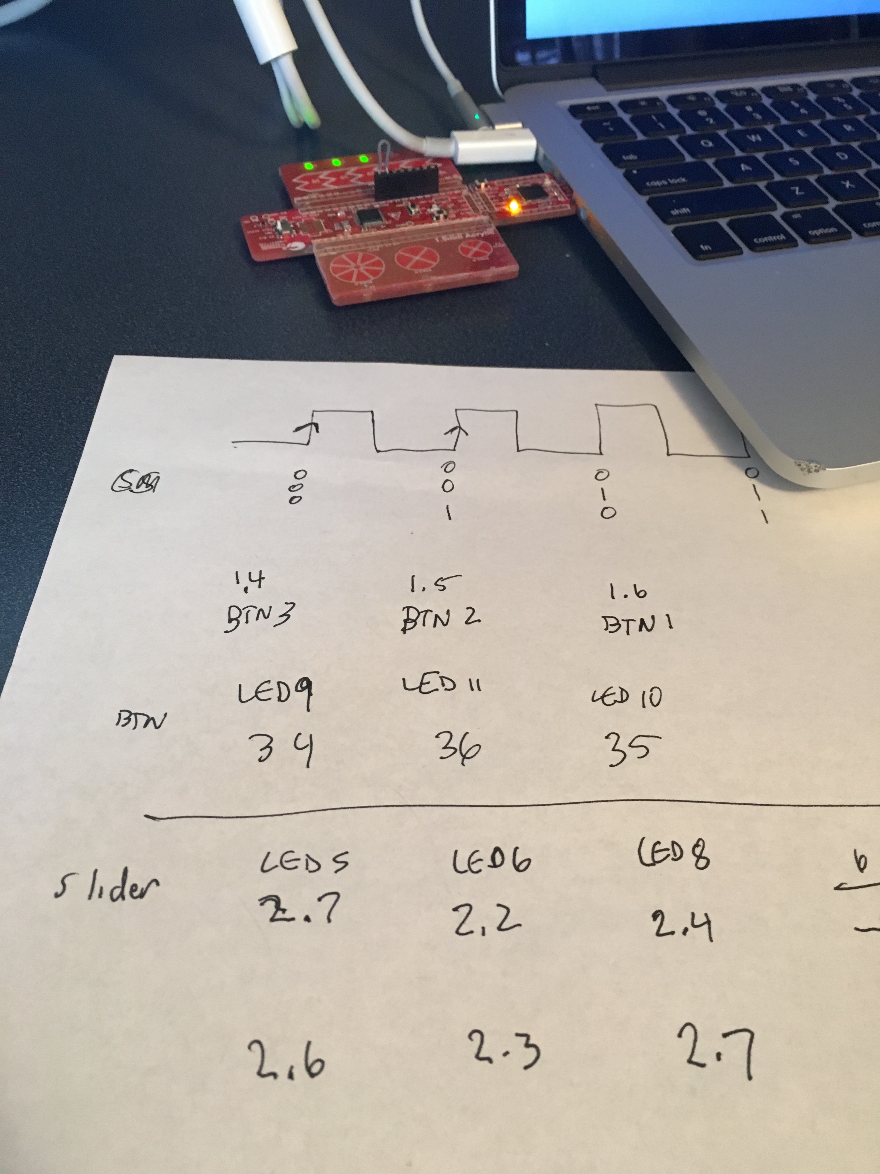
For this post, I wanted to build a simple state machine inside of the SmartIO. So I decided to build a 3-bit counter. On the CY8CKIT145 board, port 2 is mostly connected to LEDs. When you look at the picture below you can see that the LEDs on the left side of the board are easiest to see, so I decided to use them to indicate the state of the counter. You can see from my notes that I was originally considering using LED9,11,10 which are the three LEDs on the CapSense buttons board. I also considered using LED5,6,8 which are on the right side of the slider board, but I ruled all of that out because they were hard to see.
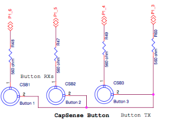
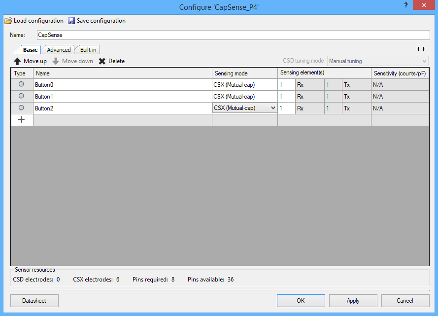
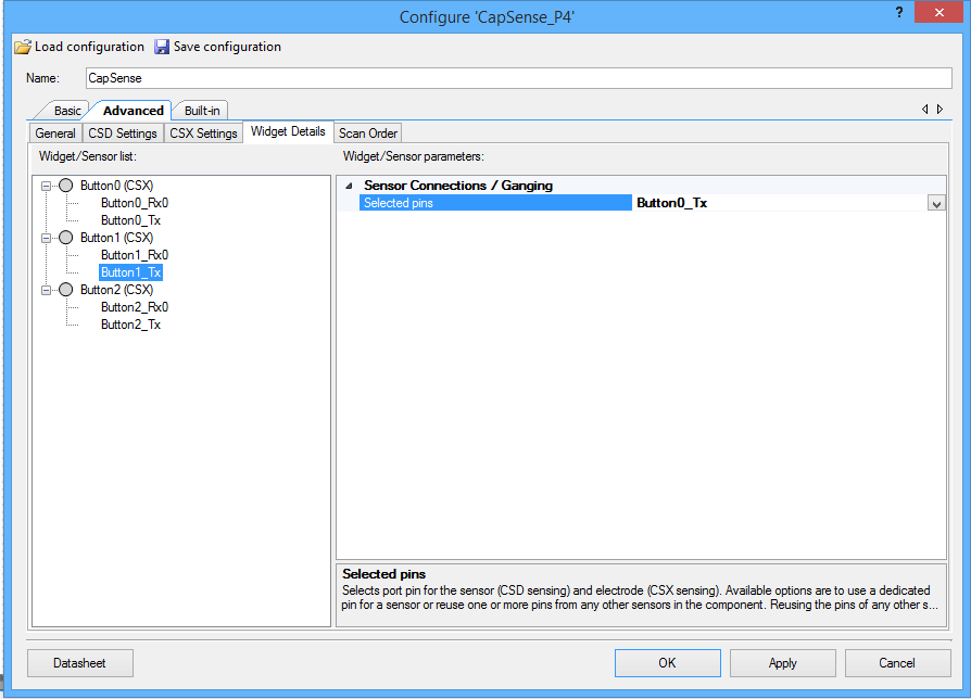
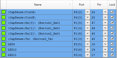
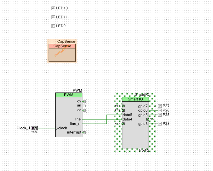
To build this project you start by creating the schematic. In this case I copied the design from the previous post called “145MutualCap” which had 3 CapSense buttons and 3 LEDs (LED10,11,9). I then added:
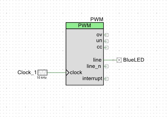
- A 5 KHz Clock to drive the PWM
- A PWM to divide down the clock to a speed that I could see and provide a clock for the counter
- A Smart IO
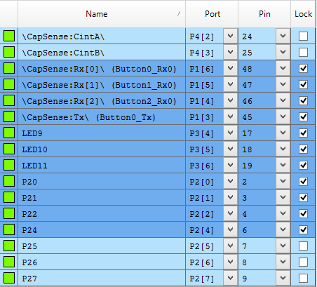
- 4 Output Pins to drive LEDs (P27, P26, P25, P23)
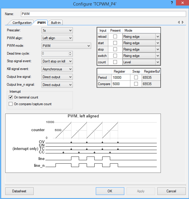
Next I configured the PWM with a 50% duty cycle and a Period of 10000. This results in a 0.5Hz clock:
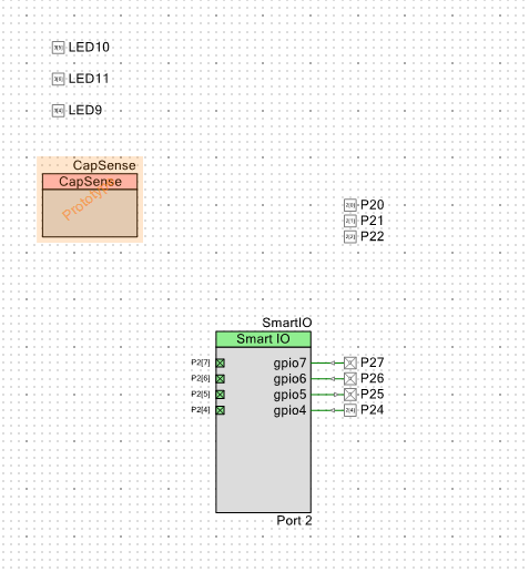
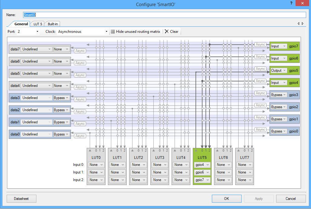
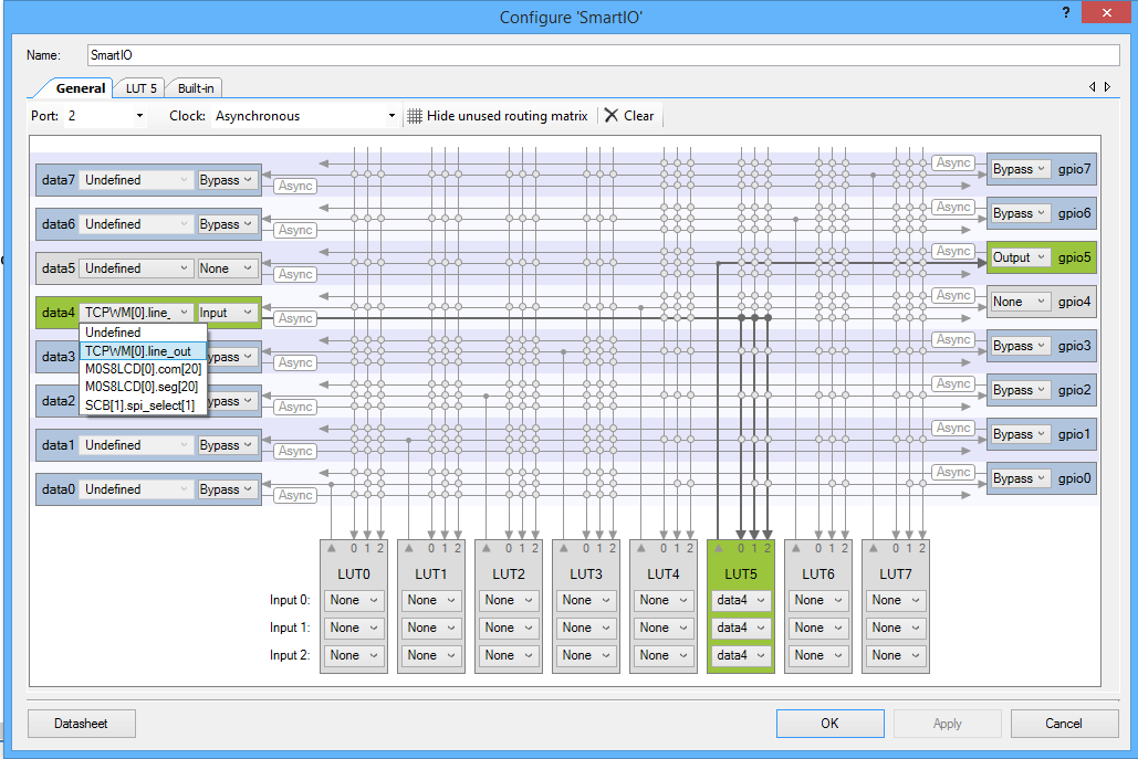
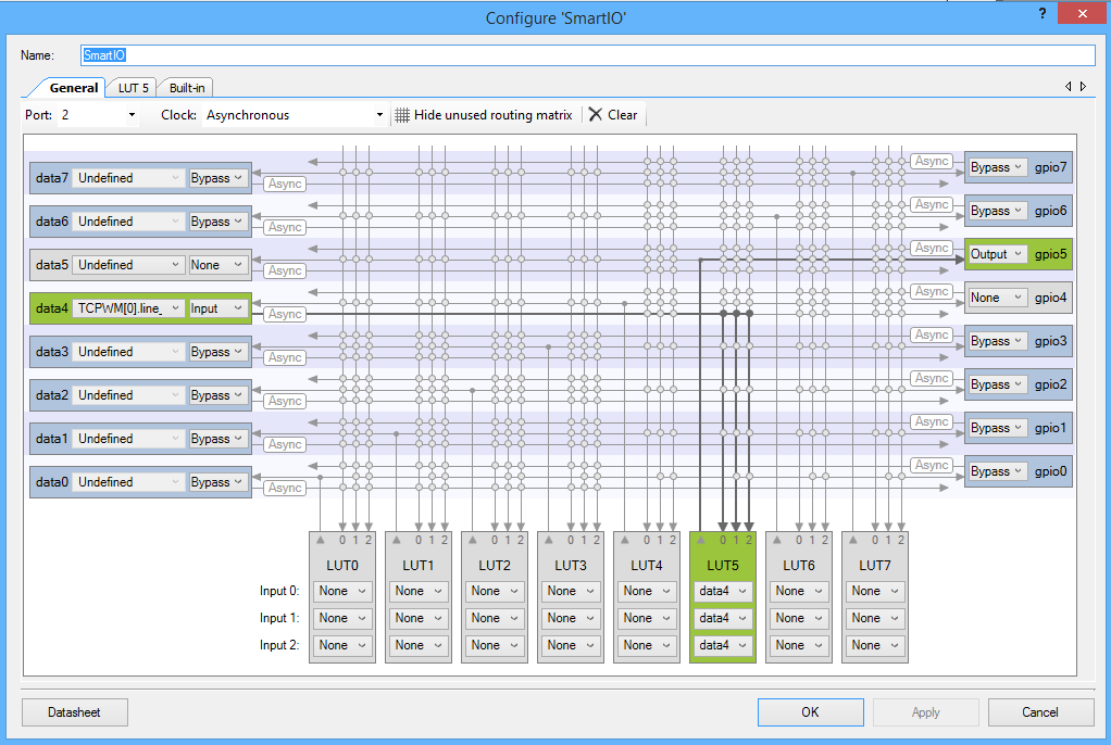
Then I configure the SmartIO.
- Setup “data4” as an input to the Smart IO. Data 4 is the line out 0 of the TCPWM0
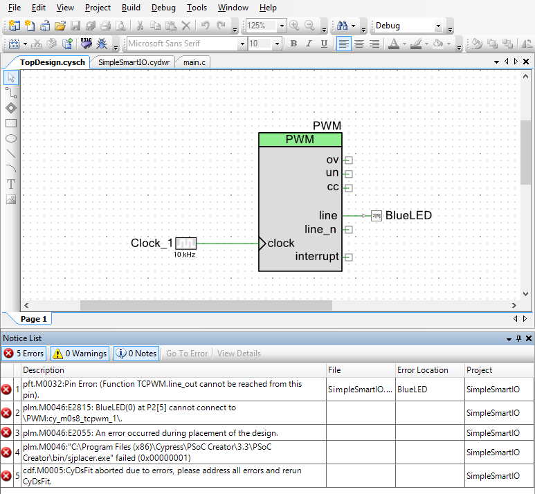
- Setup “data5” as an input to the Smart IO. Then configure it to be the “clock” for the smart IO. Data 5 is the Line_N of TCPWM0. Originally I wanted to be able to have the clock drive LED5 as well, but this can create a timing hazard in the Smart IO and is not allowed (which is why I mirror data 4 onto the output P25.
- Setup GPIO 7,6,5, and 3 as outputs (these outputs are connected to P27, P26, P23 which are the LEDs on the slider board. GPIO5 is connected to P25 that is the user LED on the main board
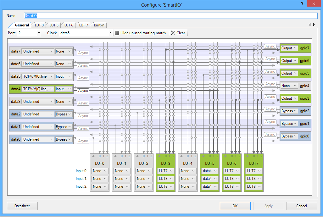
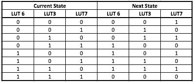
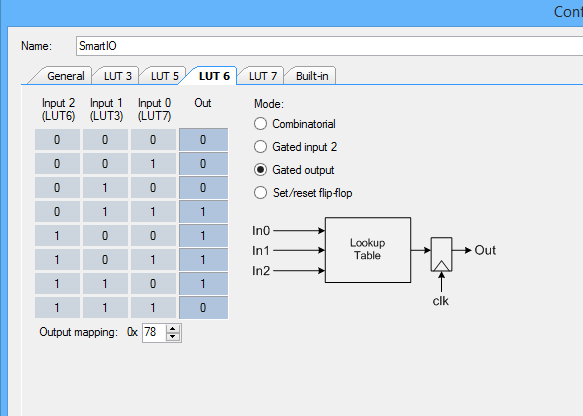
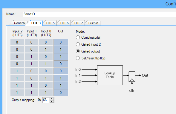
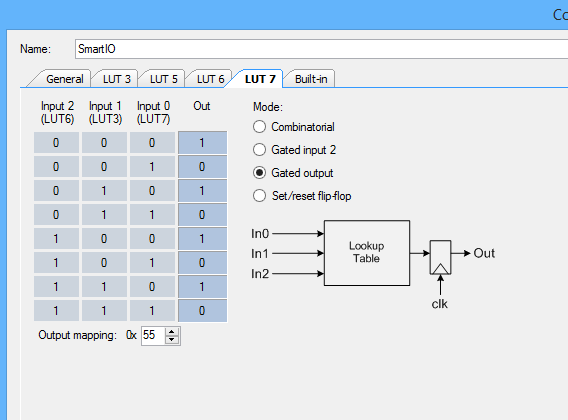
Then I configure LUTs 6, 3, 7 to implement the state table of a counter
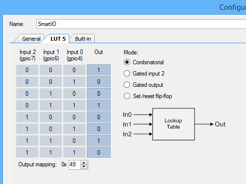
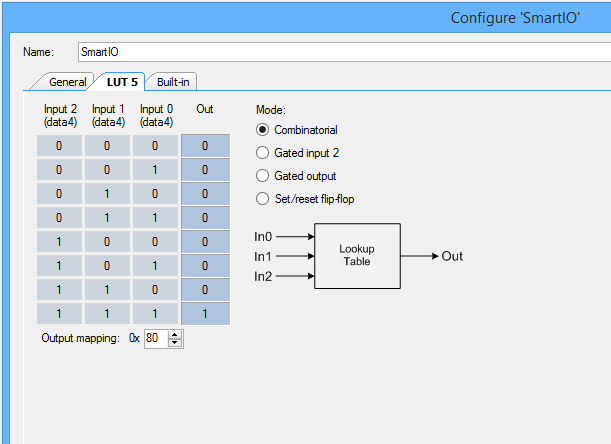
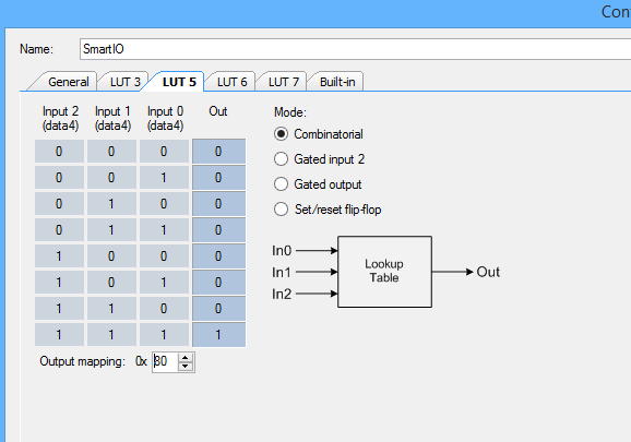
I want to be able to see the clock (the PWM input data4) ticking so I create a transparent LUT (000 = 0 and 111 = 1) for LUT5 which is attached to P25 which is the LED on the main board.
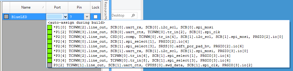
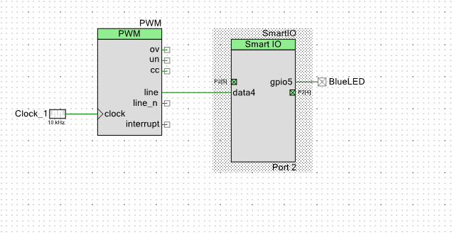
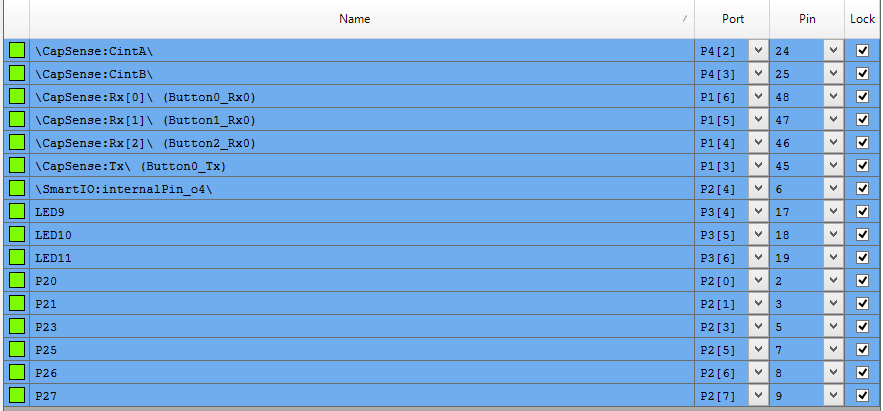
After this is done I need to assign the Pins.
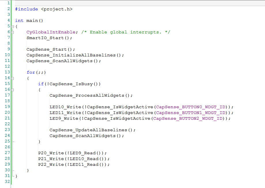
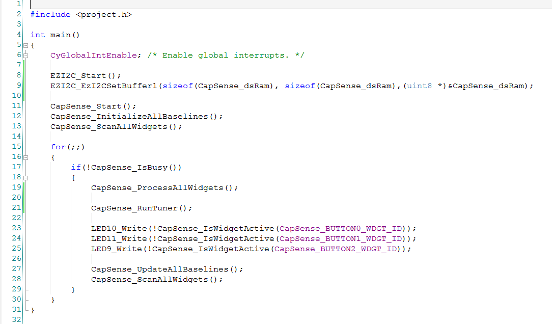
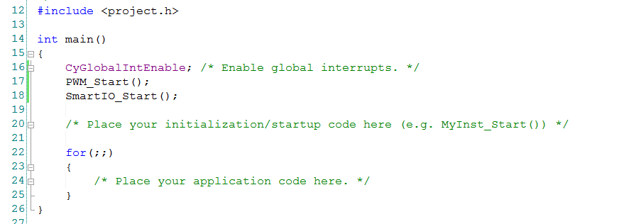
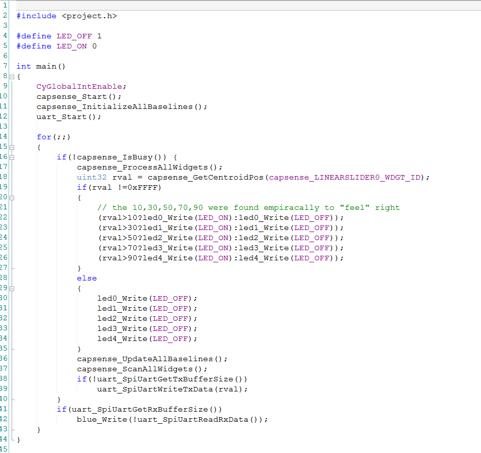
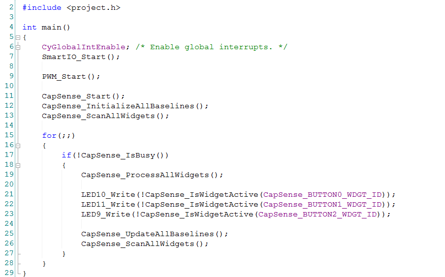
Followed by the very simple firmware which is copied from the previous design. The only new code is line 9 to turn on the PWM.
You can find this PSoC Creator workspace on github in the directory called “SmartIO”. This project is called “SmartIOCountUp”.
Index
Description
PSoC4000s & The SmartIO – Part 1
An introduction to the SmartIO and first project
PSoC4000s & CSX Mutual CapSense Buttons Part 1
Using mutual capacitance
PSoC4000s & CSX Mutual CapSense Buttons Part 2
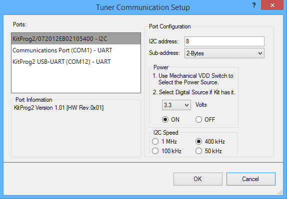
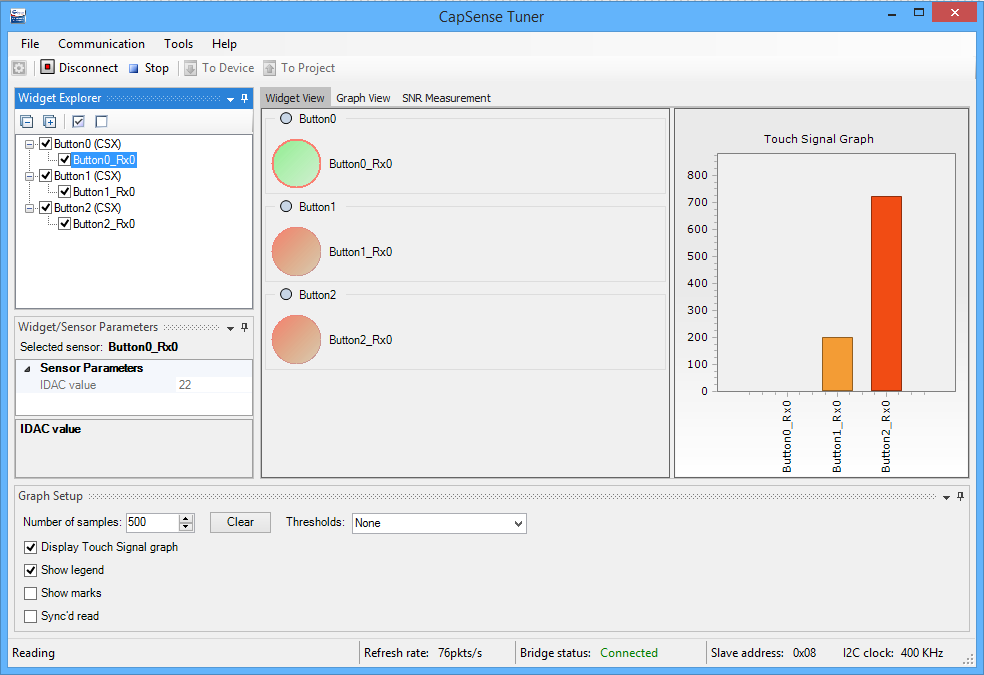
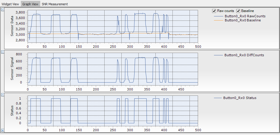
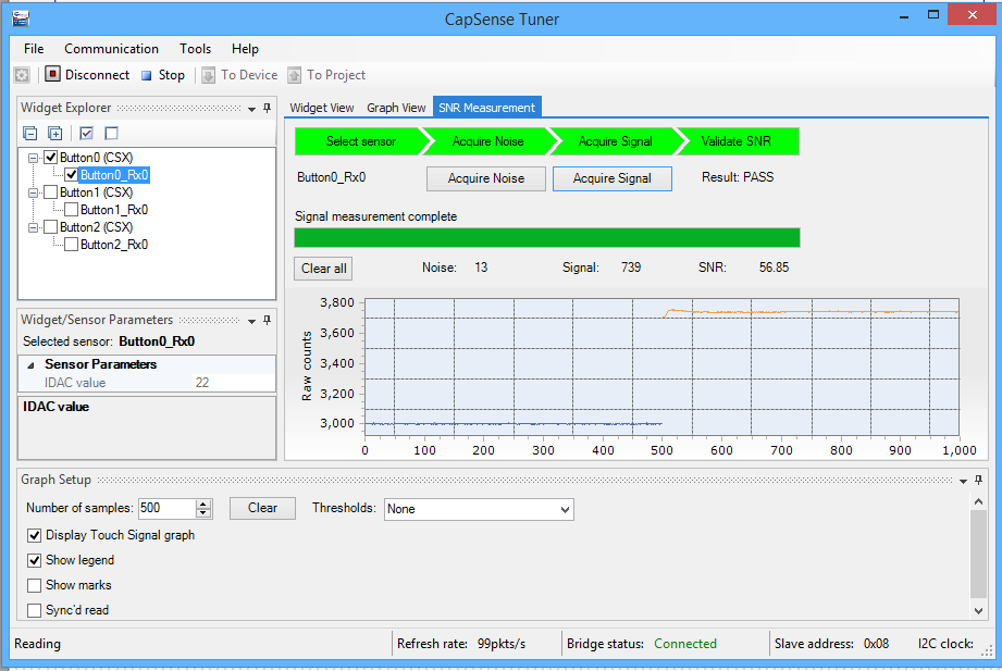
Using the CapSense tuner
PSoC4000s & The SmartIO – Part 2
A 3 input XOR logic gate
PSoC4000s & The SmartIO – Part 3
A 3 bit up counter state machine
PSoC4000s & The SmartIO – Part 4
Using an external clock with the Smart IO
PSoC4000s & The SmartIO – Part 5
Triggering an interrupt