About 2 years ago, I bought a Qinsi QS5100 reflow oven from China via Amazon.com. My decision was based almost completely on the nice youtube video that Ian Lesnet from Dangerous Prototypes posted about his results. After I got the oven, I successfully built a series of Physics Lab boards with it. Then one day about a year ago, I got two boards in a row with horrible results which I attributed to the temperature profile. A few weeks later, I dug around on the internet and decided to change to the Lesnet profile and things seemed to be working again.
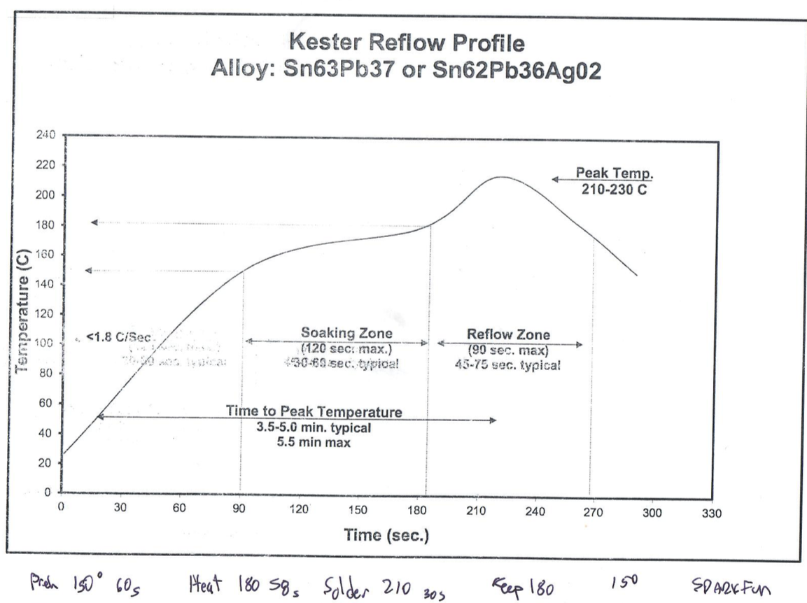
I have always had this bouncing around in the back of my head as a potential problem because I wasn’t SURE about the source of my original problem. And, I don’t really believe in magic, but I didn’t have time to pursue a root cause. As I have had a little bit of time the last few days, I decided to dig in. First, I found the data sheet for the Kester solder paste that I have been using. Here is scan of the printout of a blown up section from the datasheet with my handwritten notes from the Lesnet video (which I incorrectly denote as Sparkfun)
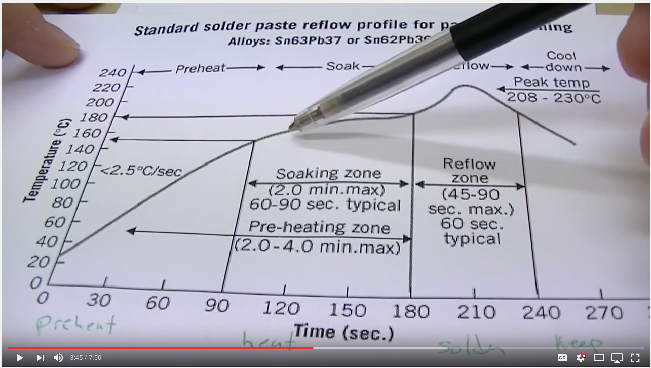
In fact in the video Mr. Lesnet shows a screenshot of a solder profile which is similar to the Kester data sheet. I wondered why he didnt use that profile?
I had switched to using the Lesnet profile and was having consistently good results. However, yesterday I decided that I wanted to compare that program with reality. I found at least a couple of places on the internet where a comparison of the actual temperature and the programmed temperature were made with a Fluke & Thermocouple.
In the past I used the Fluke/Thermocouple method as well, but I found it difficult to compare a time based profile with instantaneous readings from the Fluke. Moreover the numbers that you can read from the Kester data sheet don’t seem to match what you can enter into the QS-5100. So, what in the world is the oven doing?
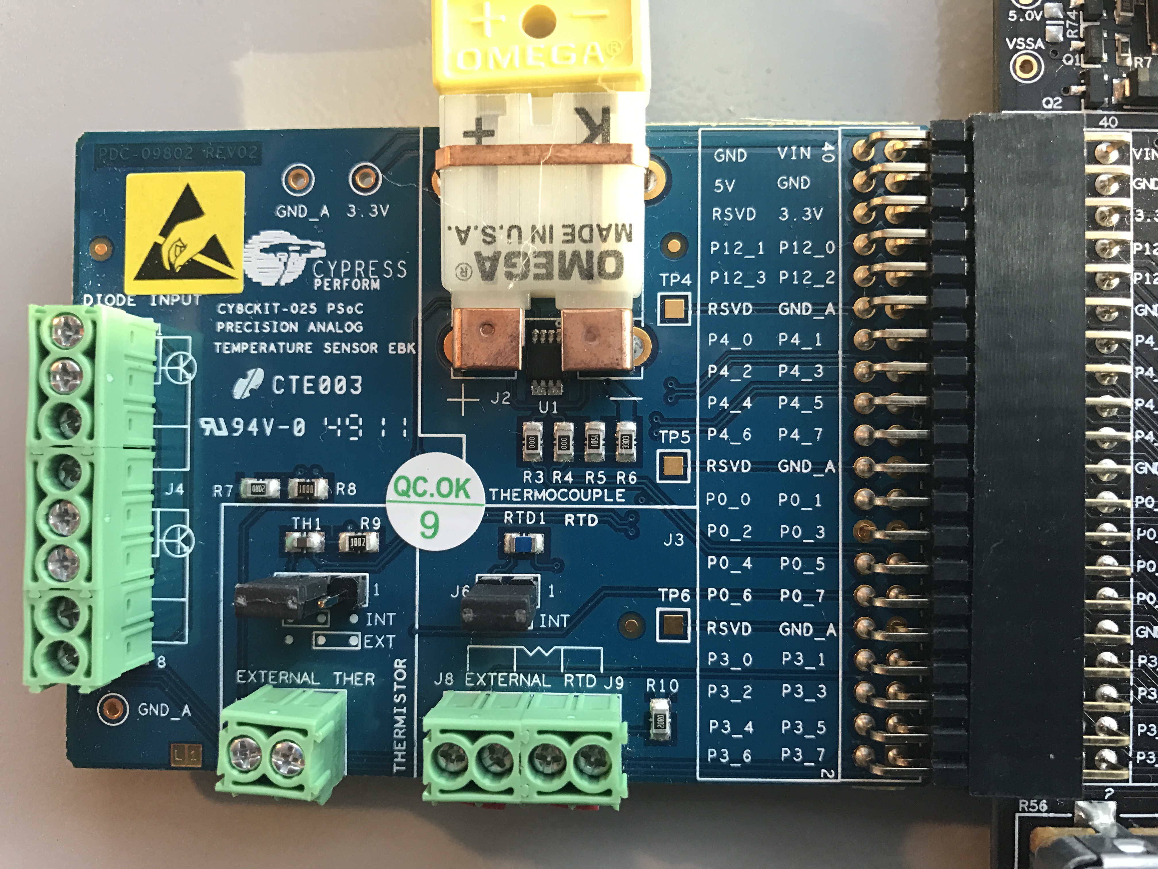
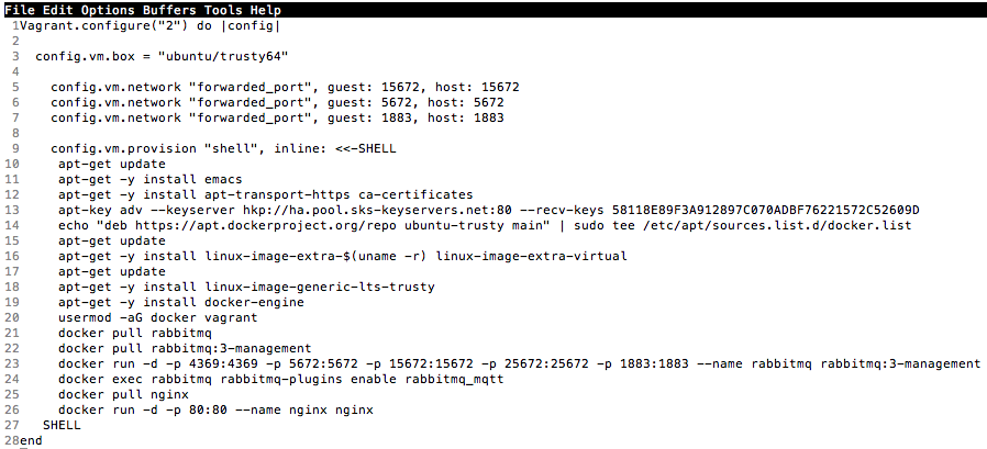
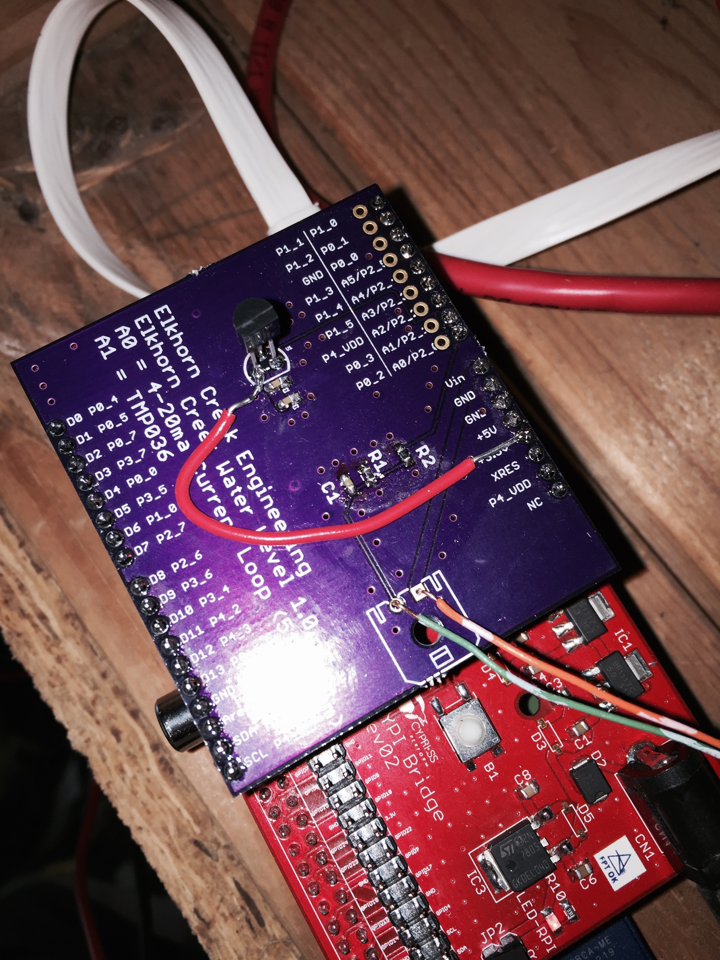
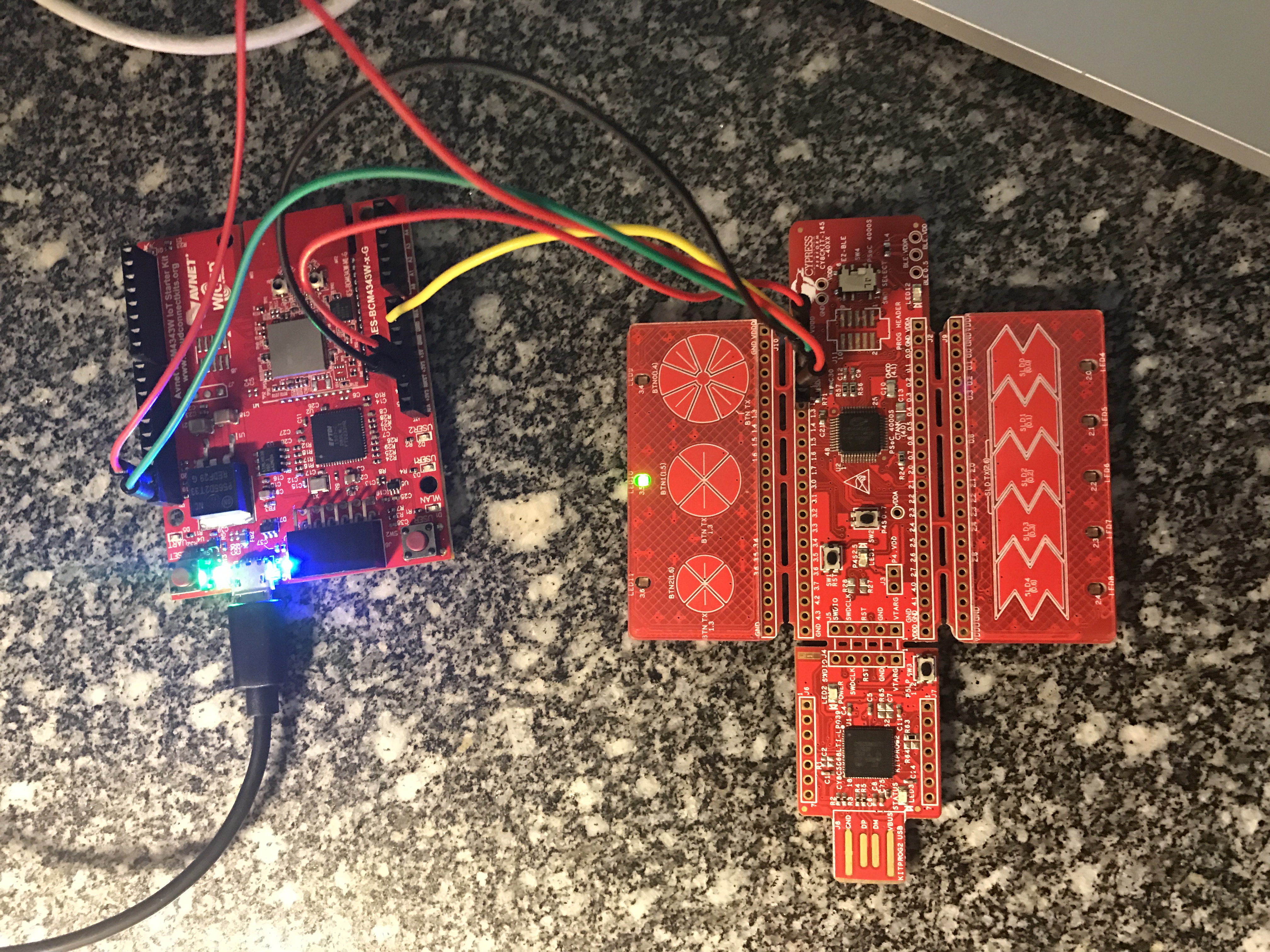
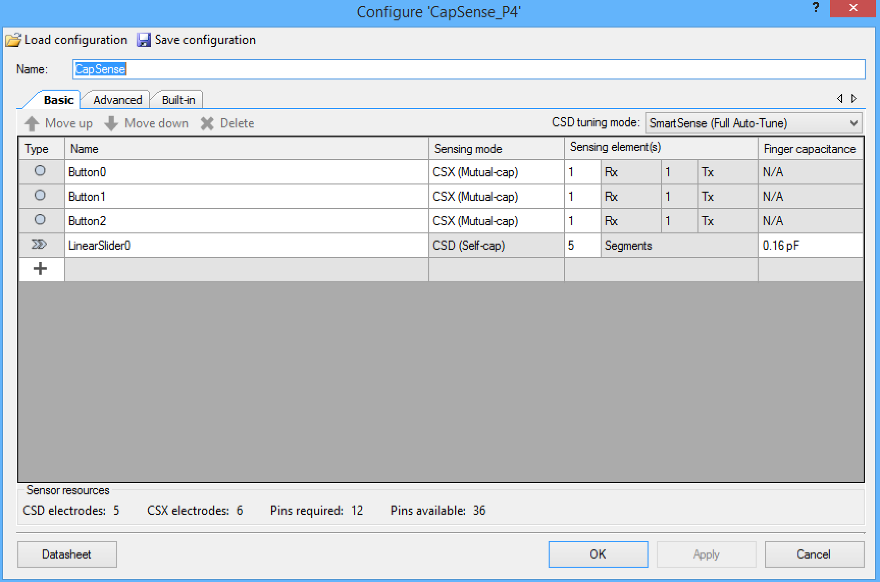
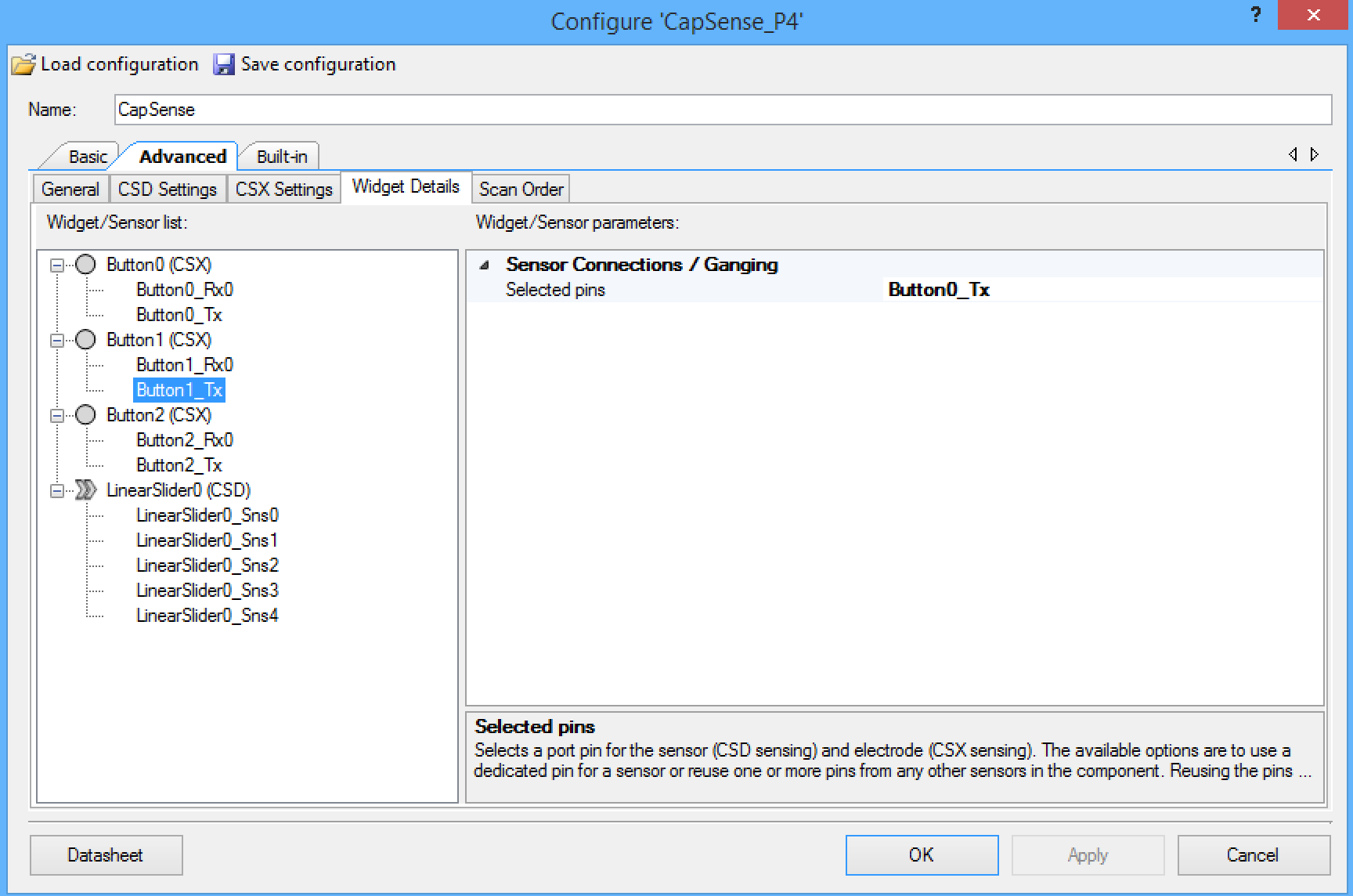
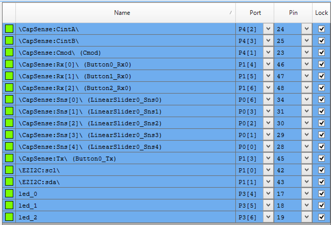
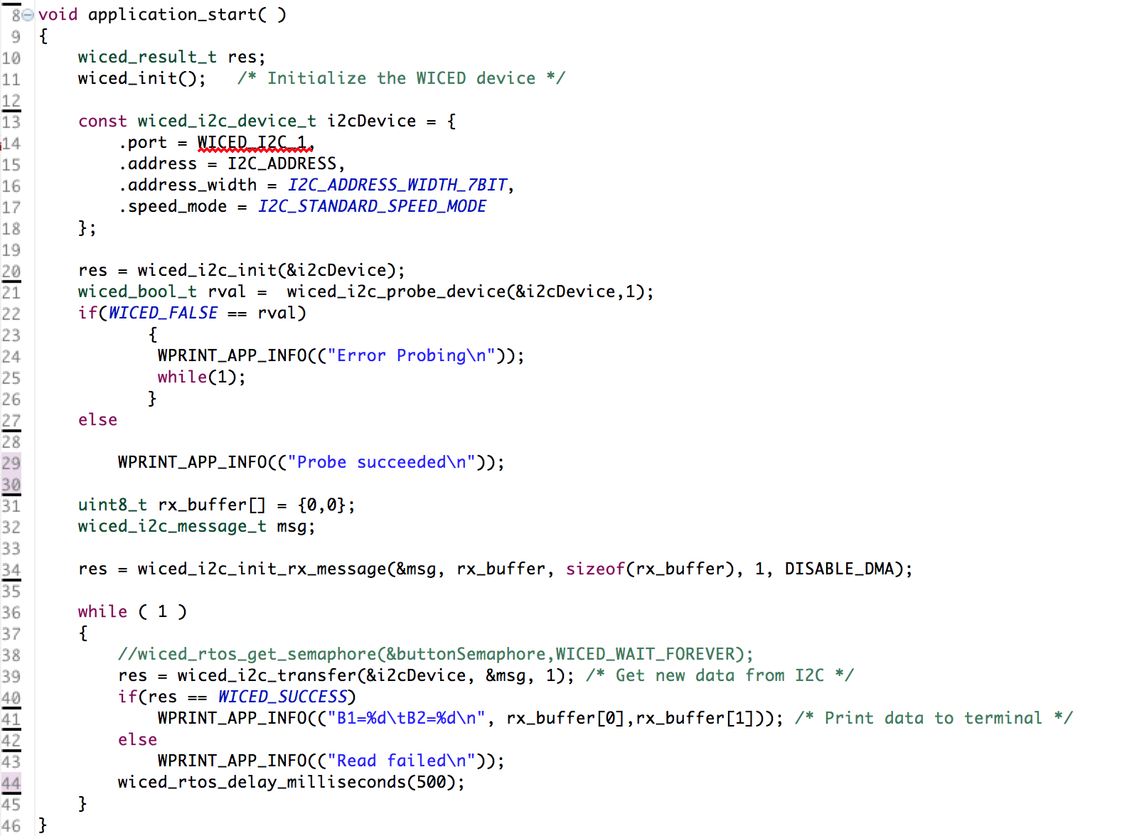
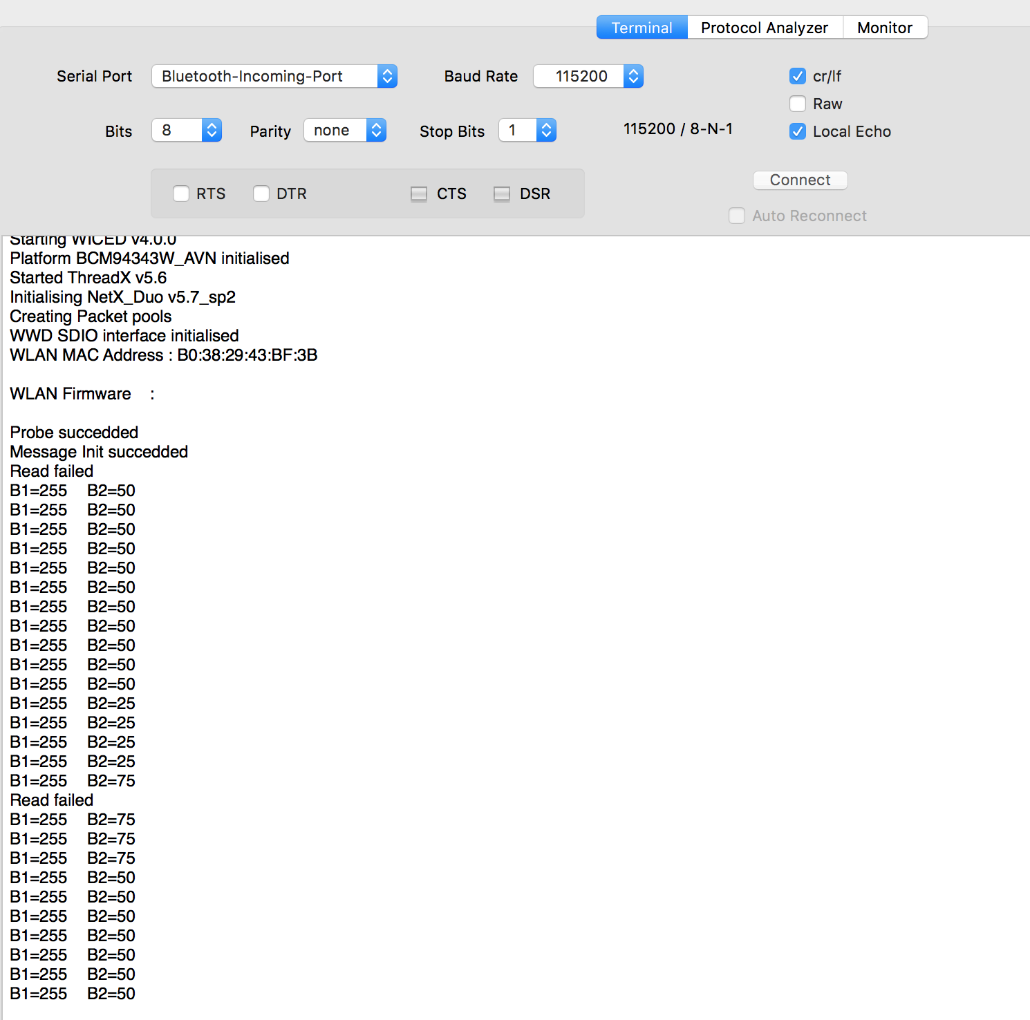
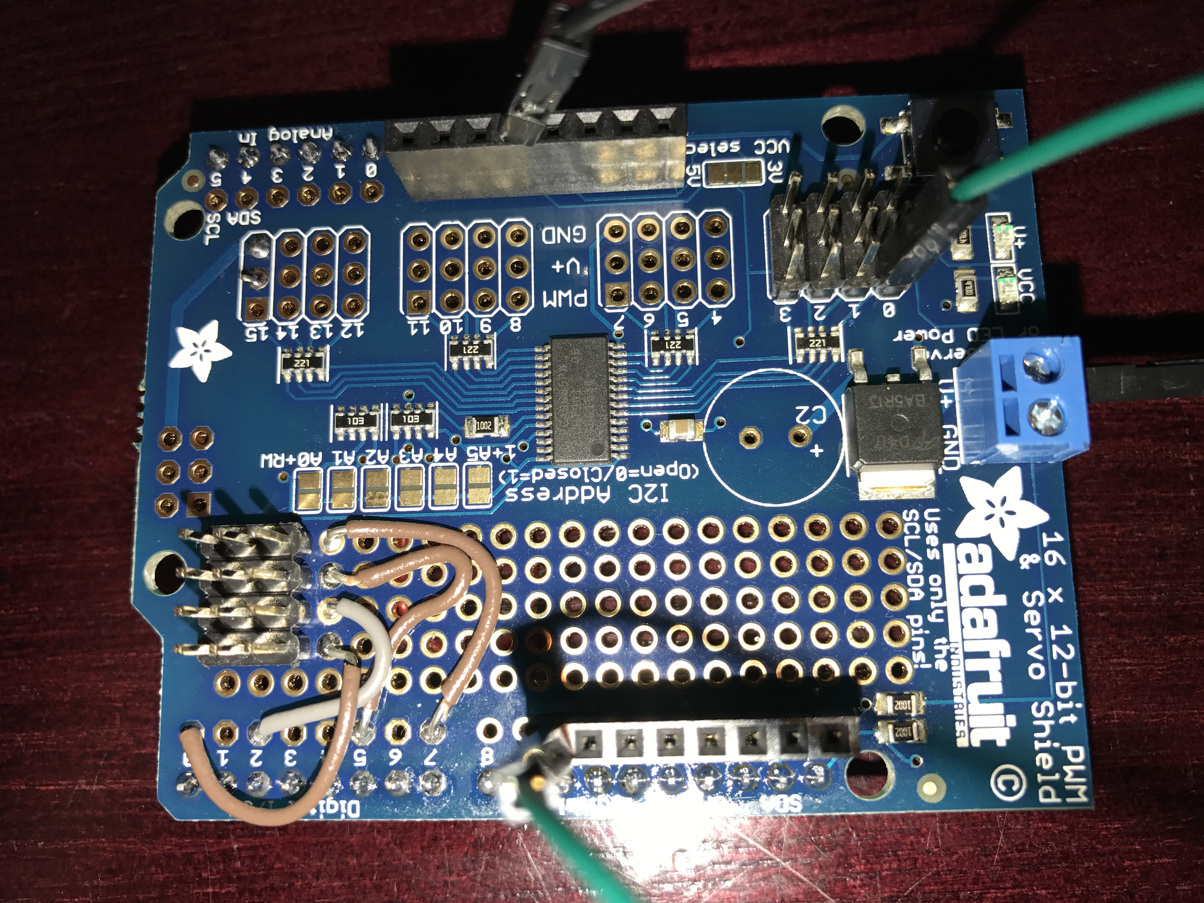
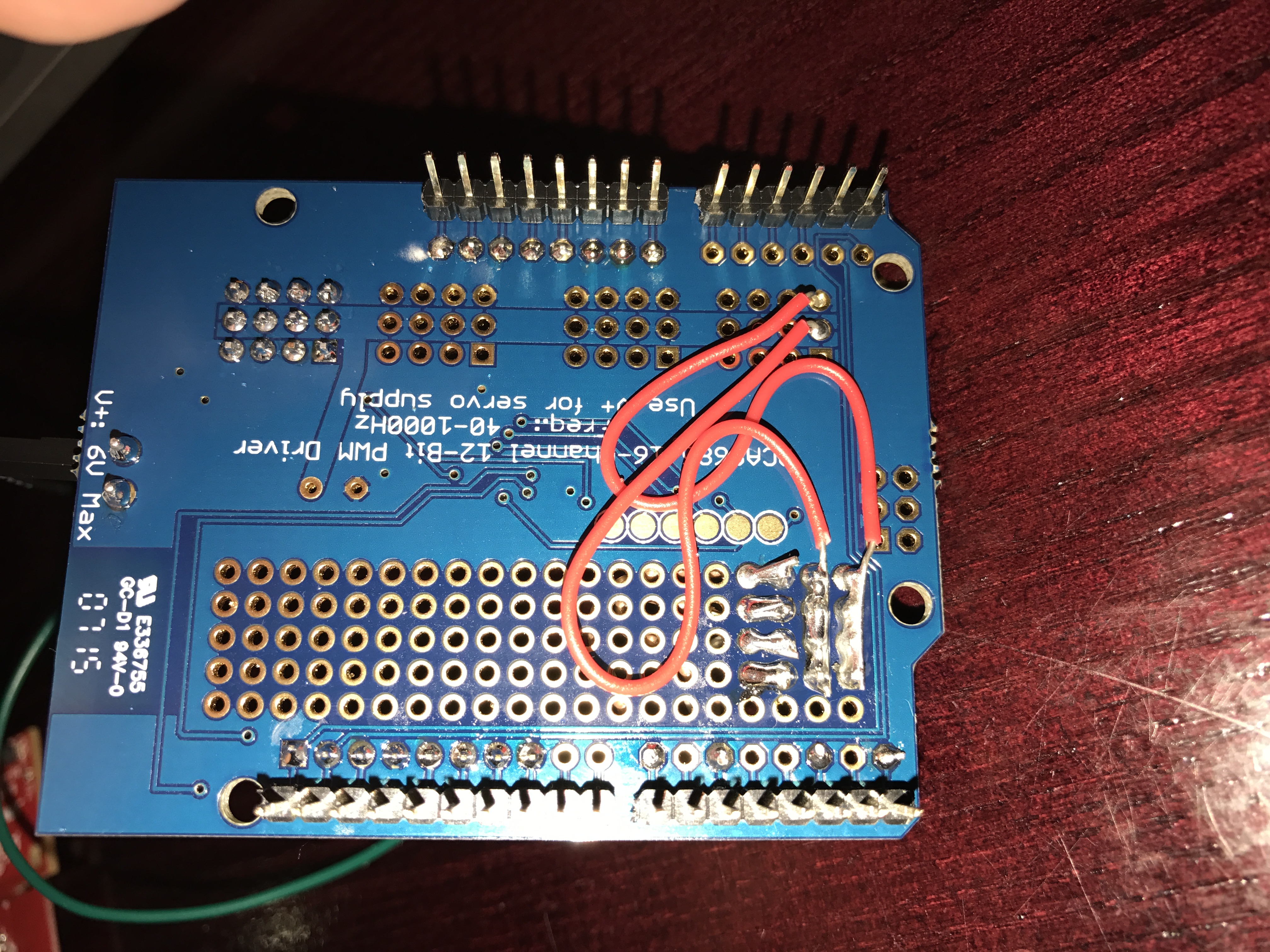
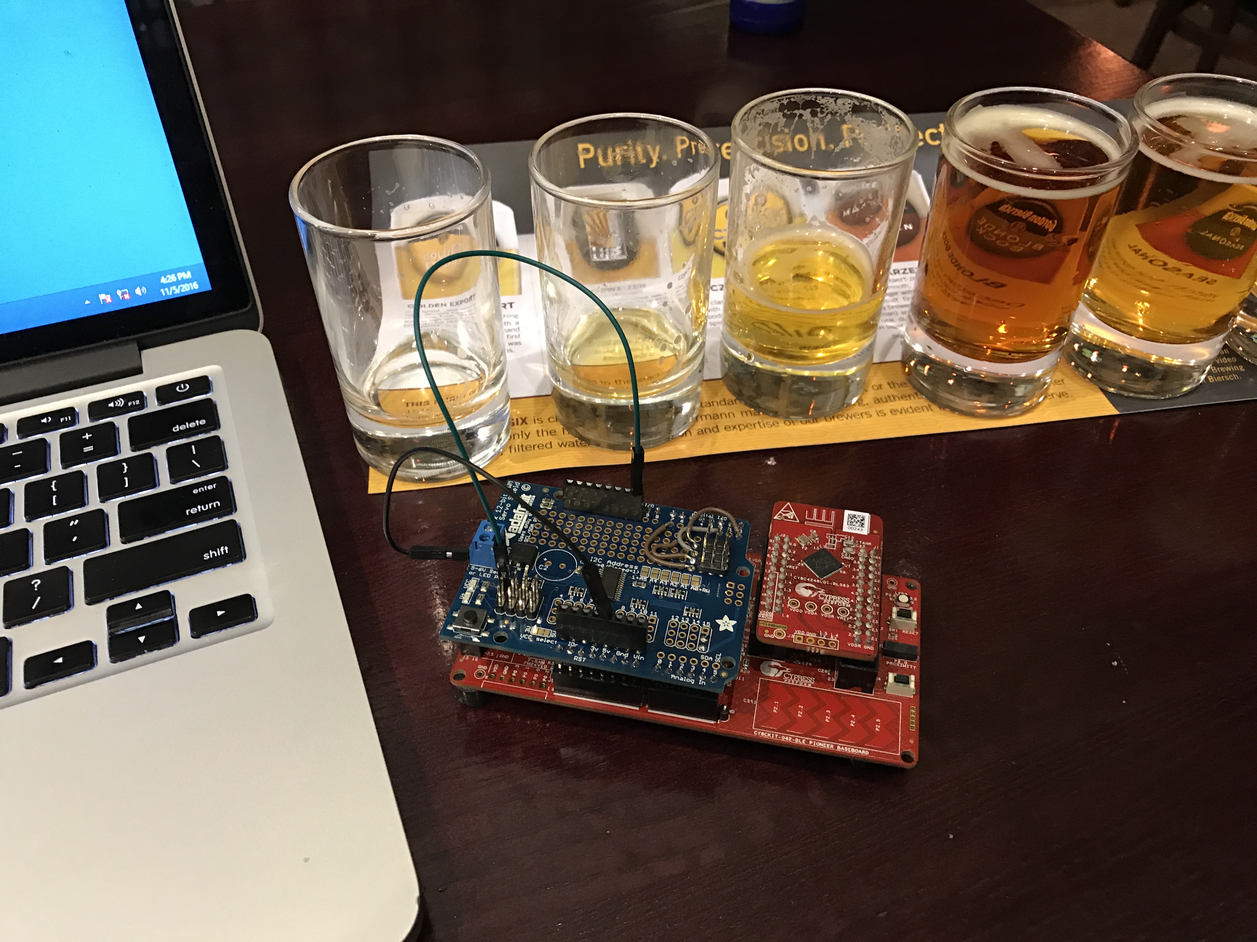
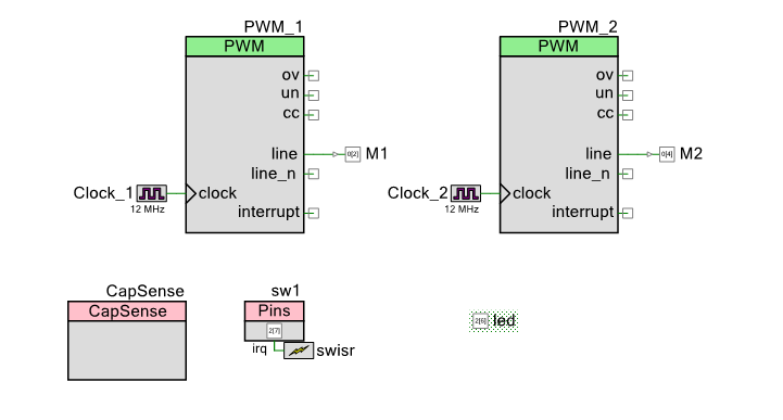
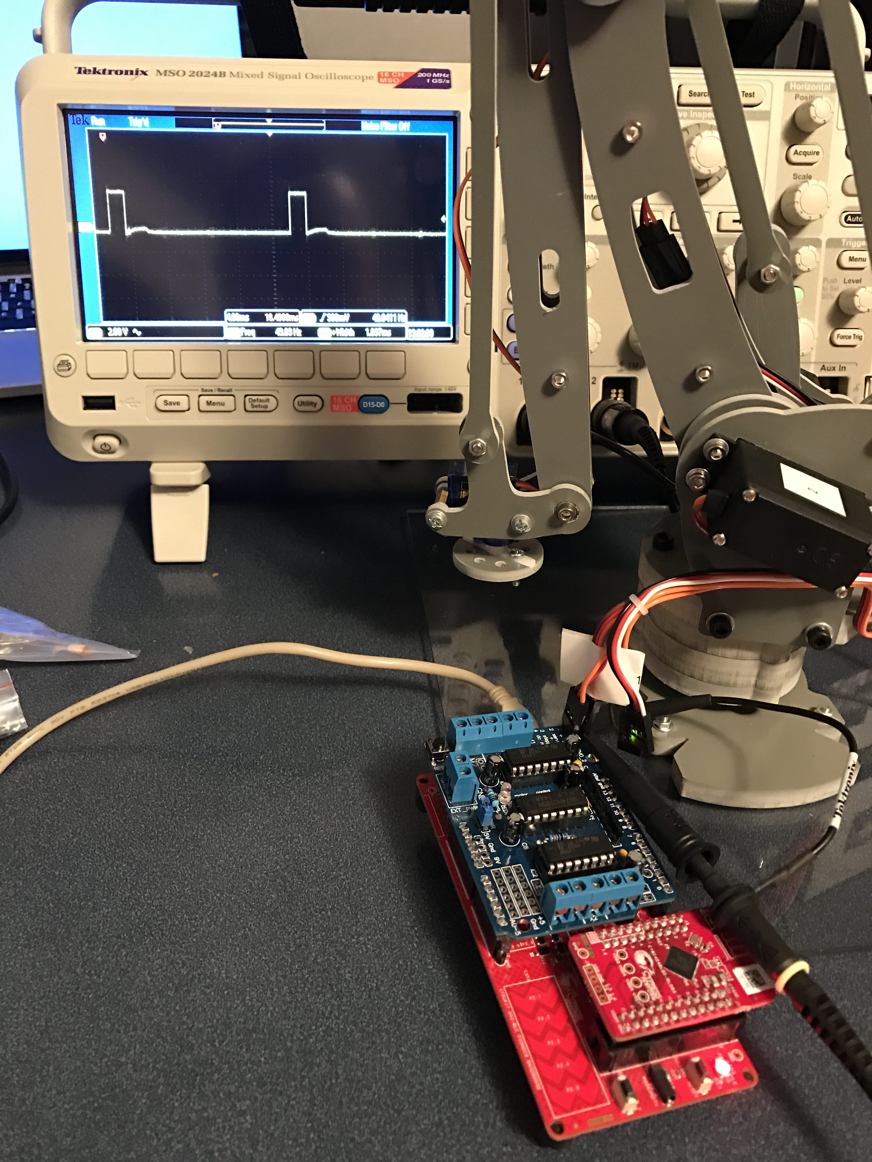
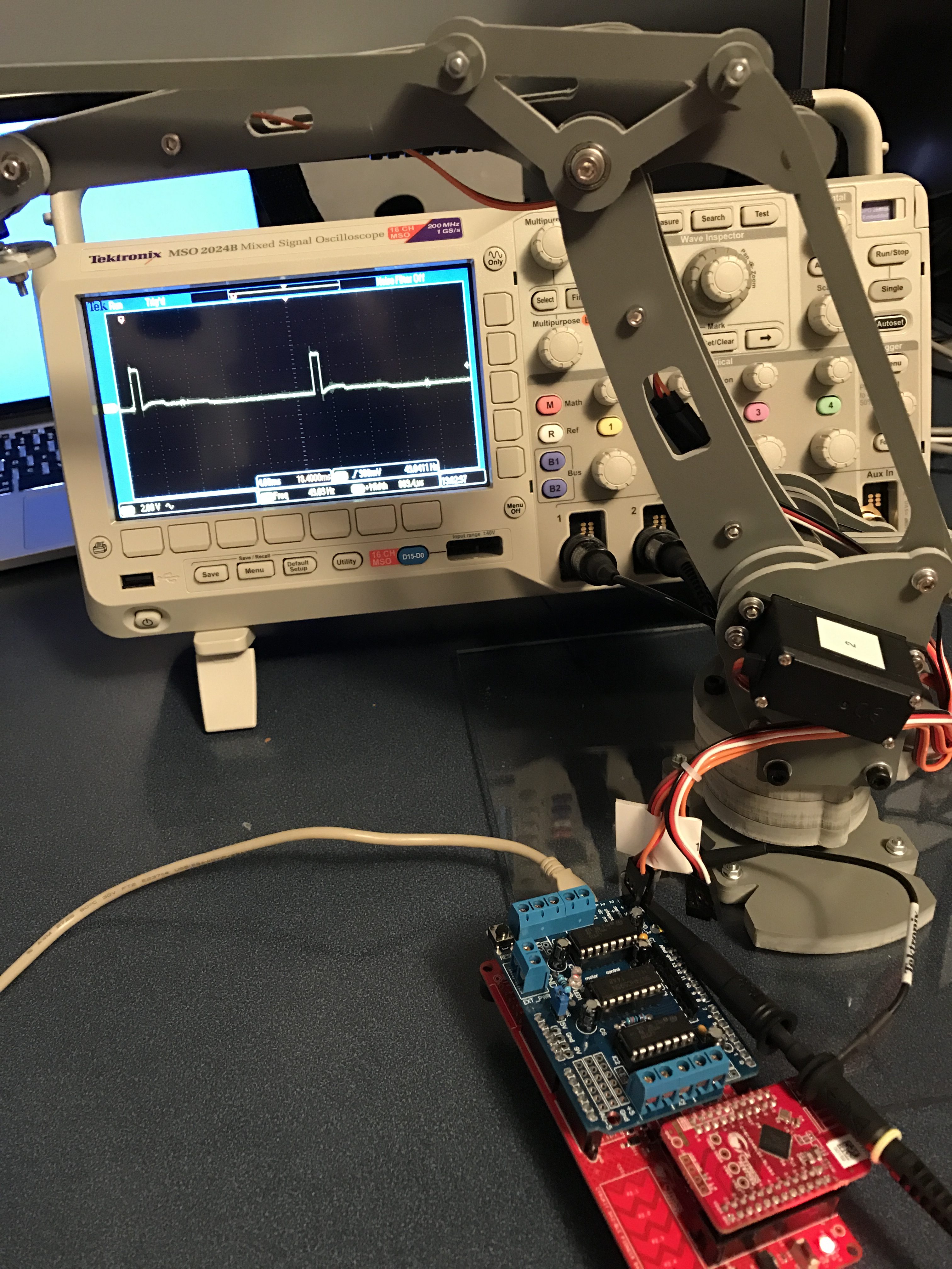
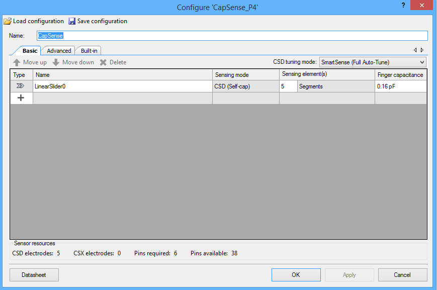
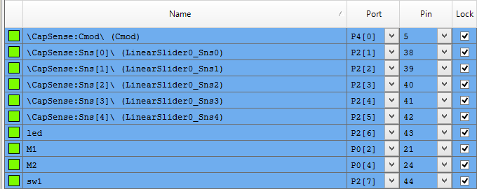
What I really wanted was to capture the data in realtime so that I could plot and analyze what the oven was doing. To do this I used CY8CKIT-025 Precision Temperature Sensor Expansion Board attached to a PSoC5LP CY8CKIT-050 connected to the Bridge Control Panel to capture the actual PCB temperature into an excel file. The CY8CKIT-025 has a K-Type thermocouple, a DS600 for cold junction compensation, a thermistor, an RTD and a temperature diode. When paired with the 20-bit ADC in the PSoC5LP you are able to demonstrate a bunch of different methods for measuring temperature. I used the example project that came with the kit with one modification, the addition of an “EZI2C”. By putting in an EZI2C I was able to use the Bridge Control Panel to measure the temperature every 100ms and record that data to a file for analysis. Here are several pictures of the setup:
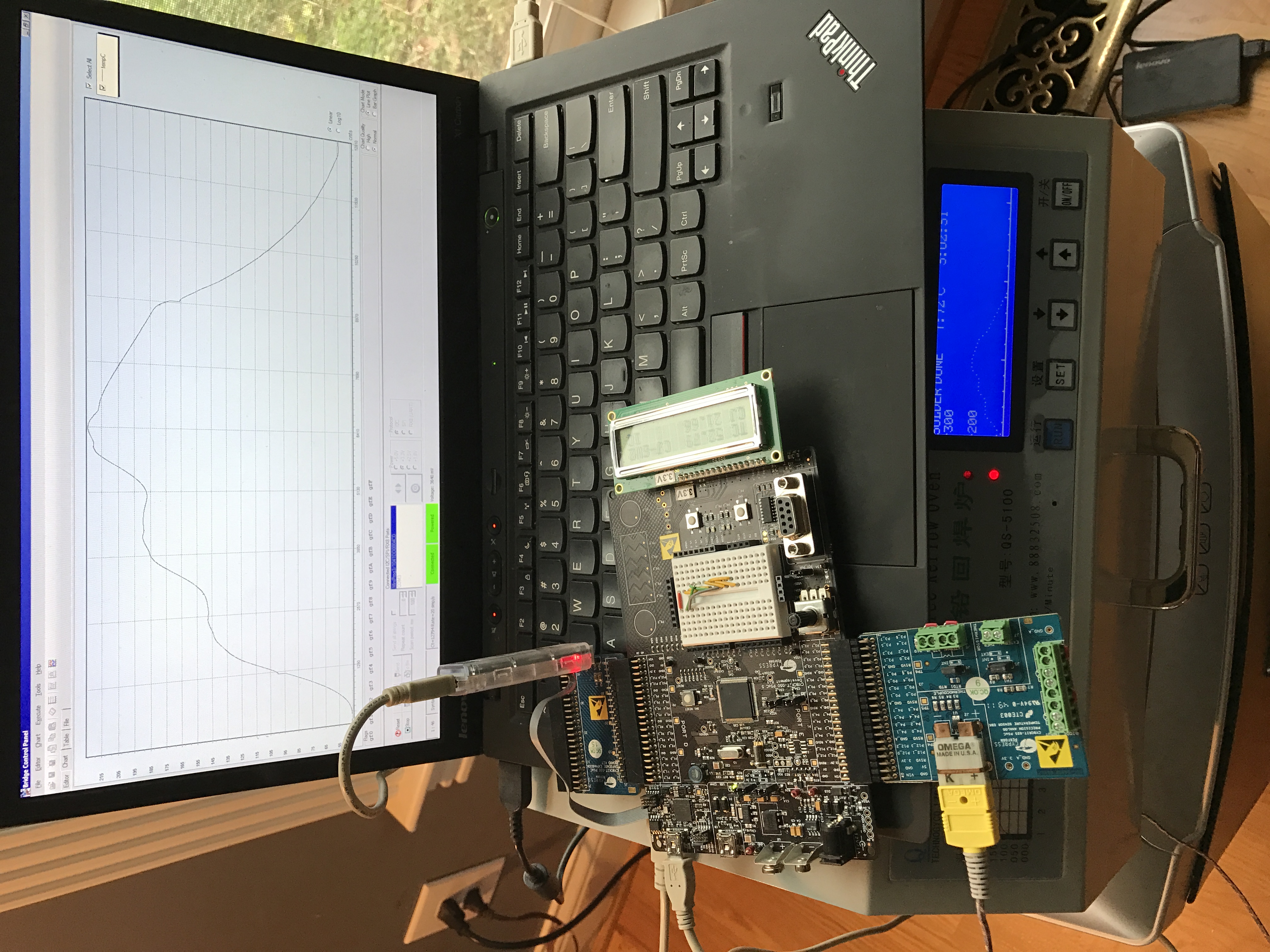
The board on the right side of the CY8CKIT-050 has a little header where you can plug in a miniprog-3 to use as an USB->I2C bridge
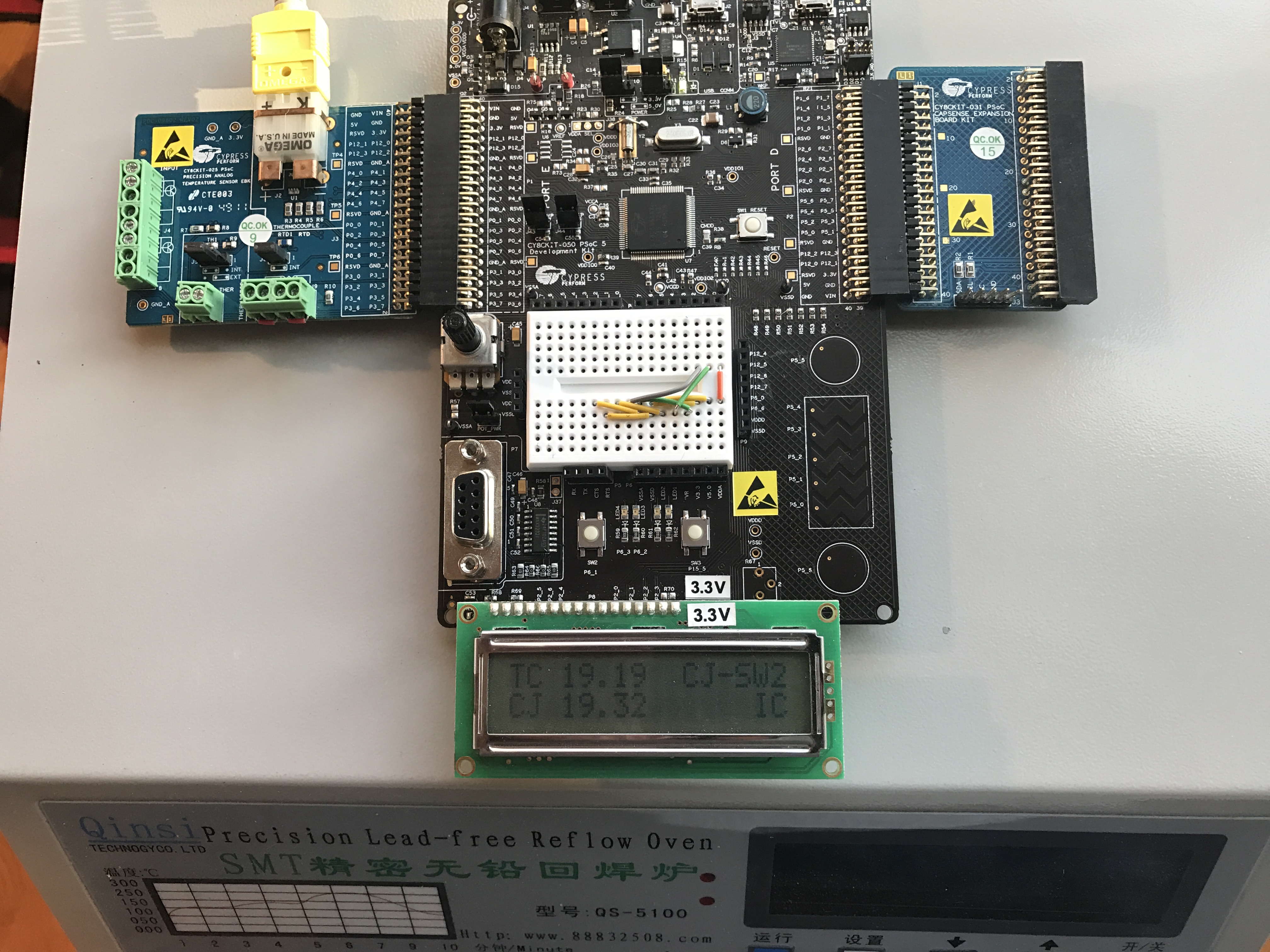
In the picture below, the PCB has been through about 15 reflows (which is why it looks so crappy). The yellow wires are holding the board and the thermocouple wire in place.
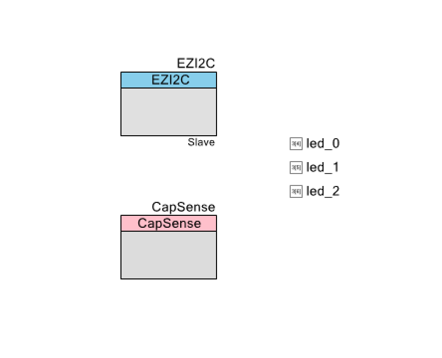
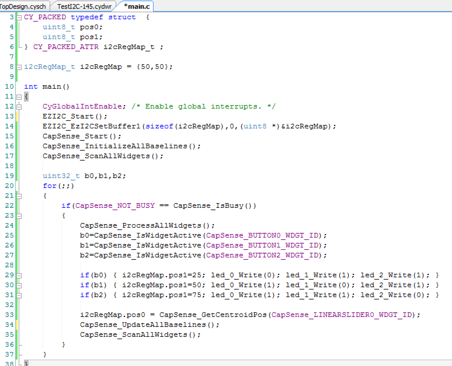
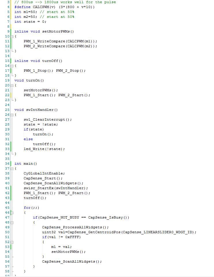
The modification that I made to the Cy8CKIT-025 kit example project were
- Add the EZI2C Component
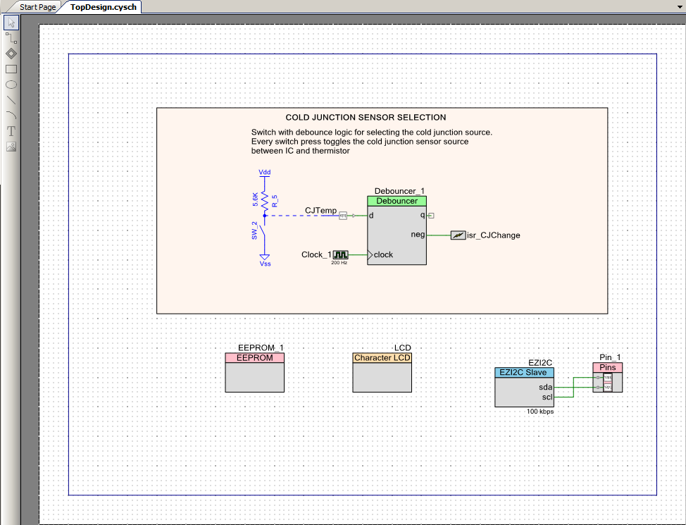
- Make a floating point buffer and attach it to the I2C
- Save the thermocouple data into the floating point buffer
![]()
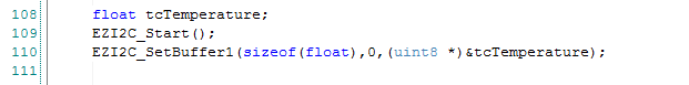
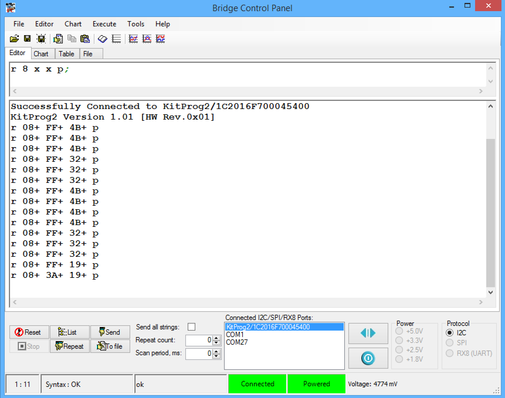
Once that was done, I can start the Bridge Control Panel and set it up to automatically read from the I2C by first setting up the variable tempC, setting up the read and then setting up the 100ms repeat.
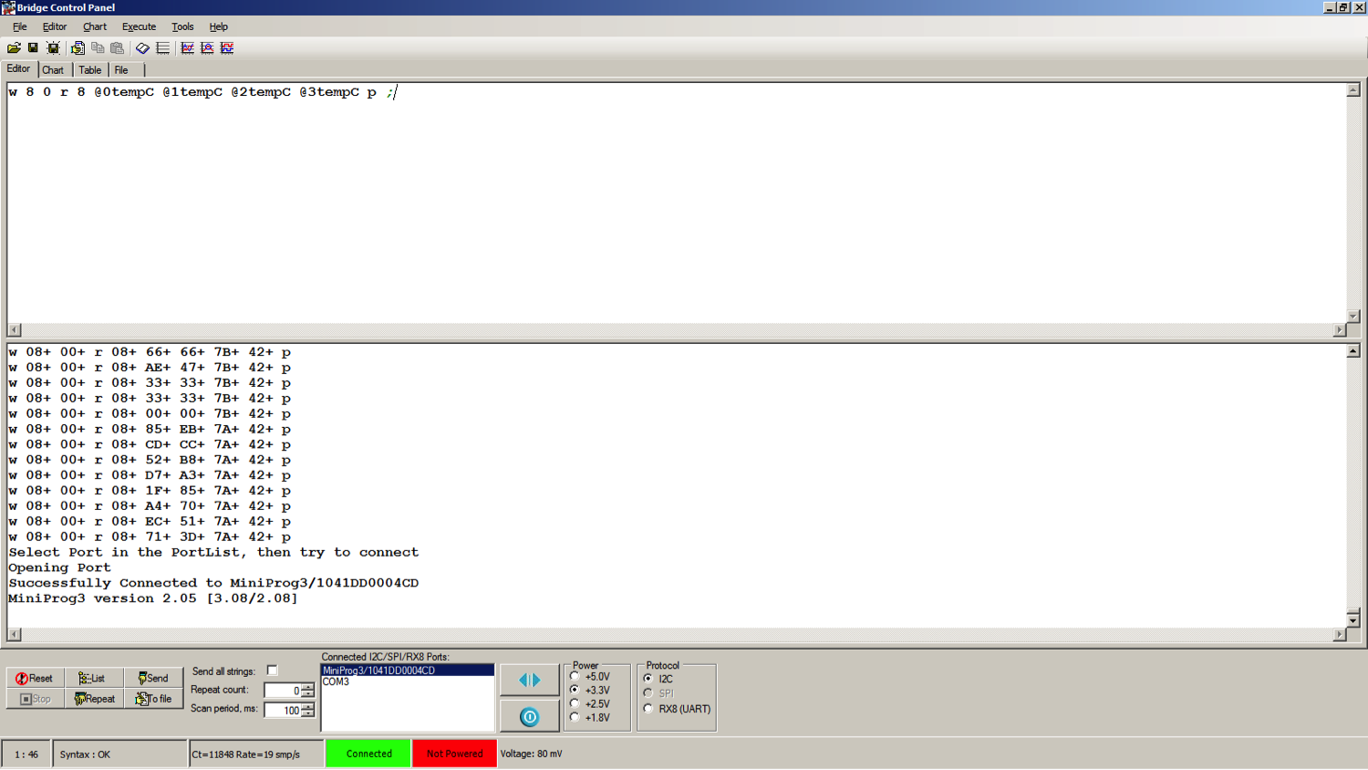
Now, I can run the whole thing and view the chart.
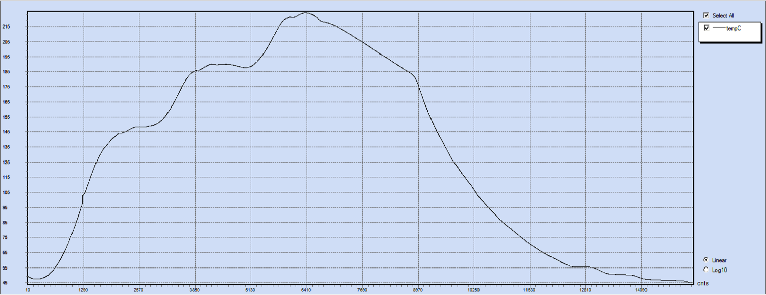
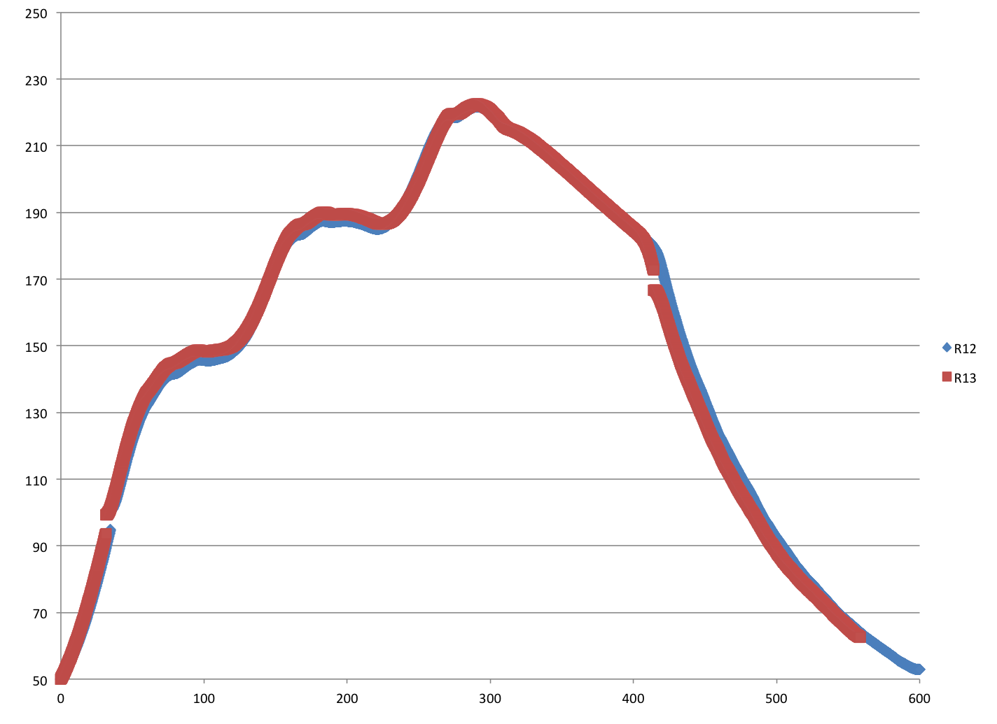
All of the temperature measurement is setup, so I can take some real data. First I look for repeatability by running a couple of heat cycles. The oven seems to act the same way every time here is an overlay of the 12th and 13th run. (bad Alan… label your axis)
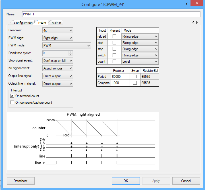
And finally we are ready to do a little bit of analysis. Here is an annotated plot of Run12 which was done with the Lesnet profile:
- Preheat 150 degrees 60 seconds
- Heat 180 degrees 58 seconds
- Solder 210 30 seconds
- Keep 180 degrees
- Cool 150 degrees
Based on the graph you can see that the oven seems to have 4 modes:
- Heat
- Hold
- Cool
- Cool with fan
In the graph below:
- The heater turns on to drive the temperature to the preheat phase (mode 1). The oven heater appears to be able to raise the temperature linearly at about 1.6 degrees C per second. Once it gets to the preheat temperature, it try’s to hold the temperature at about 145 degrees for 58 seconds (151-93) in mode 2. Looking at the graph this section isn’t very flat, so I wonder if there is really a 5th mode?
- The oven turns on the heater and the temperature ramps up to about 186 degrees (mode 1), which it then attempts to hold for about 60 seconds (mode 2)
- Then the oven turns on the heater and raises the temperature to about 219 degree (mode 1), which it then holds for about 30 seconds (mode 2)
- Then the oven lets the temperature drop naturally until it reaches about 180 degrees (mode 3)
- Then the oven turns on the fans and drives the temperature in a steeper line down to 150 degrees (mode 4)
- Then the oven turns off the fans and lets the oven cool down (mode 3)
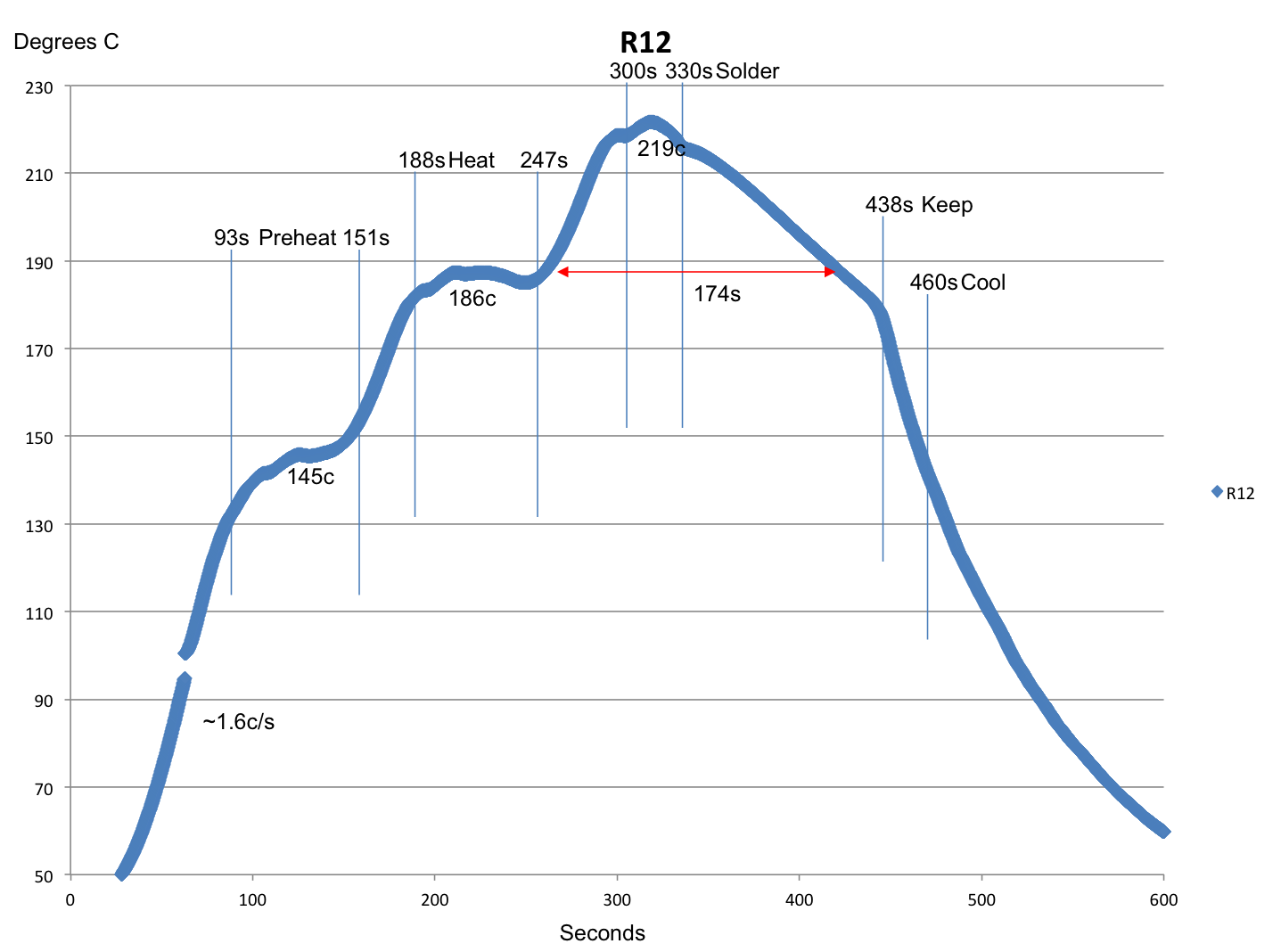
As far as accuracy goes, the time measurement seems pretty good (one website bitched about this). With regards to temperature it appears that the oven is a bit low during the preheat phase (which is also not very flat) and is a bit high during the heat and solder phases. I think that I might lower the heat/solder temperatures a little bit.. 5 degrees?
As far as matching the Kester profile goes, or the the profile on the screenshot that Mr. Lesnet showed in his video, the heat/soak phase the temperature is just a little bit high. However, he never says that his profile is intended for Sn63Pb37 solder so maybe he was trying to achieve something else (that is what I get for making an assumption). The profile does however, work very well for me for that solder. So where does that leave me?
The book that came with the oven (which is obviously translated from Chinese into very funny English) says about the same numbers for the preheat and heat and a bit hotter for the solder.
But interestingly, the oven does not come pre-programmed that way for any of the default profiles:
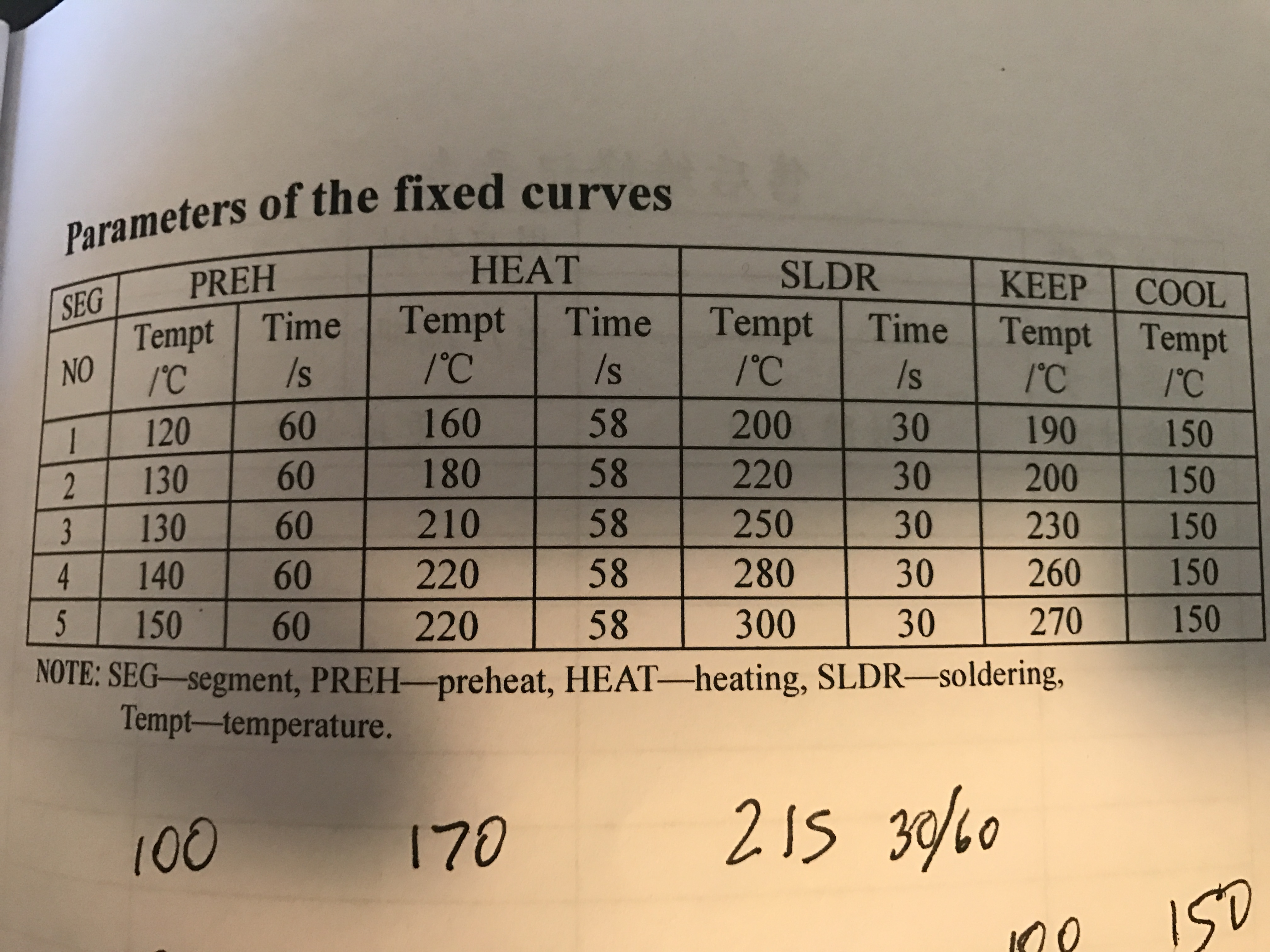
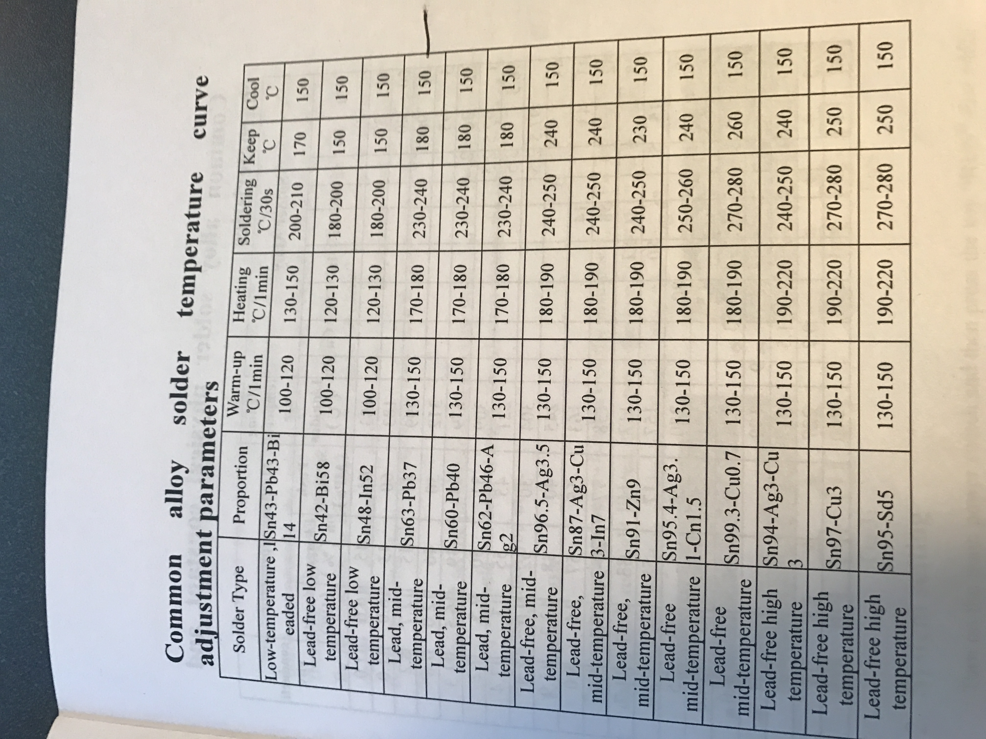
The book that came with the oven also has a nice chart with some properties of different alloys of solder. On that chart it says that the melting point of Sn63Pb37 is 183 degrees. That means that the soak/preheat phase is just below the melting point of the solder. My best guess it that the spot where the thermocouple measures the temperature-just off of the surface of the board-is actually just touch higher than the actual junction temperature which is why I think that it works.

The next real boards that I do I think that I will run an experiment and lower the preheat temperature by 5 degrees. Unfortunately that still leaves me with the question… why did I have bad solder joints originally? I think that the answer is old solder paste, but I am not sure that I will ever know.
That is it. While I was looking for information I found a number of resources on the internet to be useful
| Link | Comment |
|---|---|
| Ian Lesnet youtube video | |
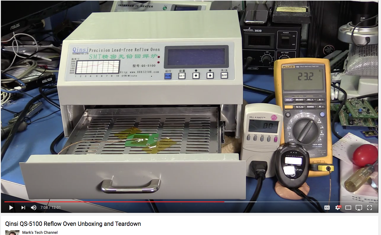
| Marks Tech Channel teardown of QS-5100 | He warns you that a wire isn't connected properly |
| Kester Datasheet | Graph profile on 2nd page of document |
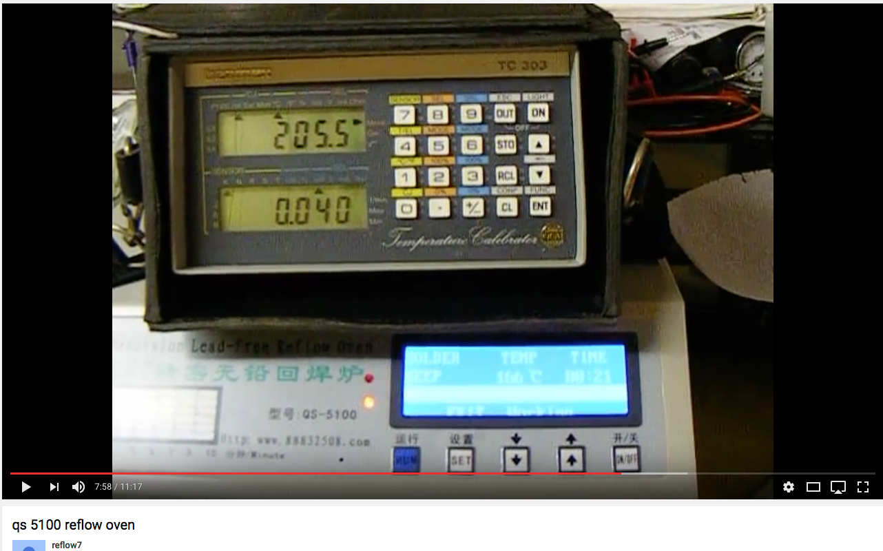
| Reflow 7 youtube video | A sweep of the temperature measured with a multi-meter |
| Dangerous Prototype Forum discussion | a few solder profiles + some proposed modifications |
| MakeICT scan of QS-5100 manual | Just a scan of the manual |
| An EEVBlog Forum discussion of the QS-5100 | A bit of chatter |
| Despectus blog teardown of QS-5100 | A modification of the placement of the thermocouple |
| Labitat wiki | A few different reflow profiles & instructions |


