Summary
Before I finish this series there are two more issues which I would like to address. First, I want to walk you through the schematic and show you how things are connected. And second, I want to talk about the “Update Scheme”. Unfortunately, there are a couple of other things that I would like to dig into, but for now this article will be the last. But, I will leave a few links at the end of the article which will give you a hint about other things that I might be interested in.
Electrical Interface
If you follow back through the previous articles you will notice that there are several different pins. Here is the pin assignment from PSoC Creator.
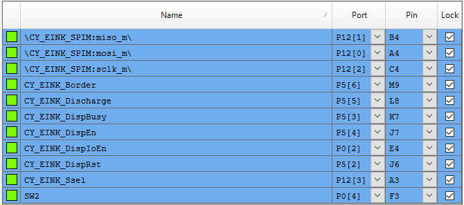
But what do they do? If you look at the list you will see that four of them are to control the SPI interface to the G2 display driver. (miso, mosi, sclk, CY_EINK_Ssel). The rest of them Ill go one by one through.
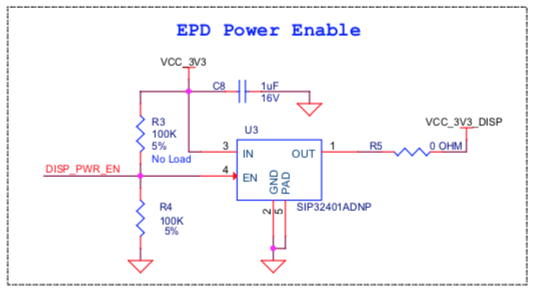
First is the pin called “CY_EINK_DispEn”. This pin really should have been called “DISP_PWR_EN” so that it matched the actual shield schematic. This is a digital output pin which is connected to a Vishay sip32401a 1.1 V to 5.5 V, Slew Rate Controlled Load Switch. Simply a power switch for the display. Notice in the schematic that there is a 100K pulldown resistor connected to the enable which means that by default the power is off to the display. Also notice that R3 is a “No Load” pullup resistor. You could remove R4 and load R3 to make the power on by default… which I don’t think that you would actually ever do as if you are using an EPD you probably care about power.
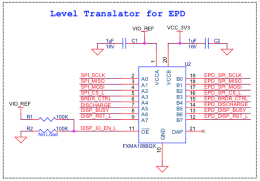
The next pin is called “CY_EINK_DispIoEn”. This is a digital output pin which is connected to “DISP_IO_EN_L” on the shield. This is simply the I/O enable of a Fairchild FXMA108BQX level shifter. This allows the PSoC to run at lower voltages (e.g. 1.8v) than the 3.3v required by the EPD G2 driver chip. This would also enable a chip to run at a higher voltage (e.g. 5V) if you were using a 5V capable PSoC (e.g. all of the PSoC 4s). The schematic uses the same pullup/down scheme that was used on the power switch above.
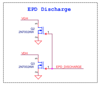
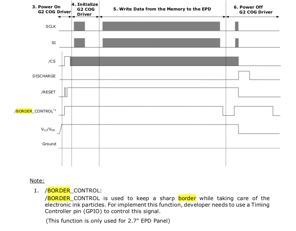
The next pin is called “CY_EINK_Discharge” and is a digital output from the PSoC. Notice that when the PSoC drives this pin high that it will enable two power transistors and will short “VGH” and “VDH” to ground.
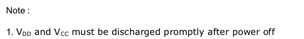
If you read the “E-paper Display COG Driver Interface Timing for 1.44”,1.9”,2”,2.6” and 2.7” EPD with G2 COG and Aurora Mb Film” document you will see this note:
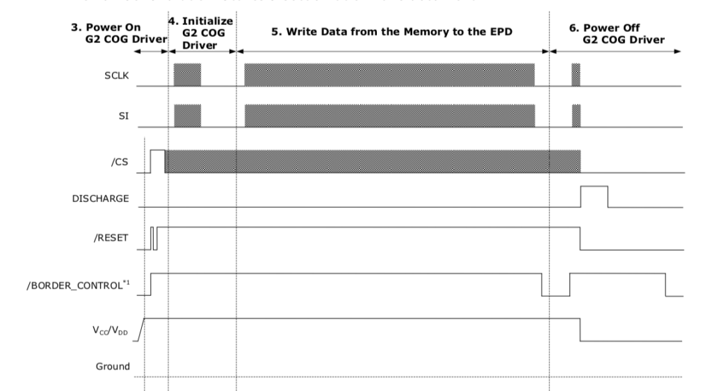
And a bit later on in the documented you will see this logic diagram.
According to the data sheet, Vgh is driven to >12v and Vdh>8v by a charge pump while talking to the screen. What I don’t understand is why the note says to drive “Vdd and Vcc” to ground when their schematic says Vdh and Vgh. I am assuming that the note is an error and the schematic is correct, but Ill send them a note and ask. [edit: I got a quick response from an excellent FAE at Pervasive… with this answer]
“No, the expression of Note 1 about Vcc/Vdd, it means the power off command set. You can also refer to Power off sequence in section 6 on page 34 of 4P018-00 as follows”
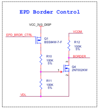
The last digital I/O pin is called “CY_EINK_Border”. This pin is connected to the note “EPD_BRDR_CTRL” on this little circuit on the shield.
If you look in the documentation you will see this note:
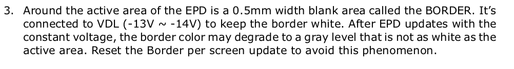
And when you look at the timing diagram you see this which shows that after you have update the frame, that you need to do a low, high, low of the border to make it white again.
This transition is handled for you by the function “Pv_EINK_HardwarePowerOff” function… which I chopped out a little bit of to show the border control.
pv_eink_status_t Pv_EINK_HardwarePowerOff(void)
{
.....
/* After E-INK updates, the border color may degrade to a gray level that is not
as white as the active area. Toggle the Border pin to avoid this phenomenon. */
CY_EINK_Delay(PV_EINK_DUMMY_LINE_DELAY);
CY_EINK_BorderLow;
CY_EINK_Delay(PV_EINK_BOARDER_DELAY);
CY_EINK_BorderHigh;
...
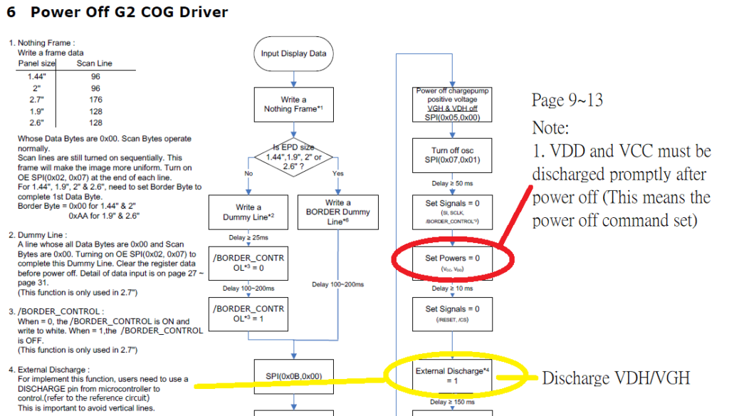
turn of the G2
....
/* Detach SPI and disable the load switch connected to E-INK display's Vcc */
Cy_EINK_DetachSPI();
CY_EINK_TurnOffVcc;
/* Return the pins to their default (OFF) values*/
CY_EINK_BorderLow;
CY_EINK_Delay(PV_EINK_CS_OFF_DELAY);
CY_EINK_CsLow;
CY_EINK_RstLow;
CY_EINK_DischargeHigh;
CY_EINK_Delay(PV_EINK_DETACH_DELAY);
CY_EINK_DischargeLow;
/* If all operations were completed successfully, send the corresponding flag */
return(PV_EINK_RES_OK);
}
Update Scheme
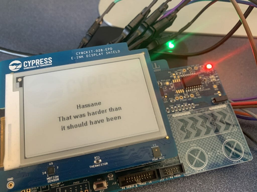
If you look at the original picture that I posted, you can see that “Hassane…” text. But if you look closely you can see a “ghost image” of the Cypress logo in the background. Why is this?
It turns out that Pervasive has three schemes for updating the screen they are called
- Four stage
- Two stage
- Partial
The four stage update actually writes four complete images on the screen as below (here is the picture from the Pervasive document)
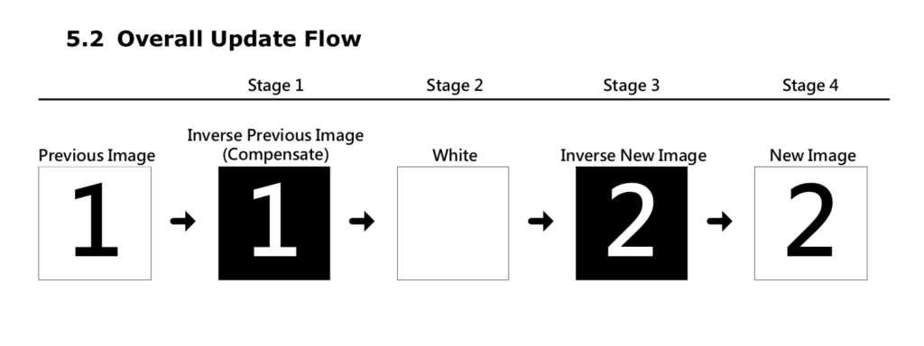
The purpose of this four stage update is to reduce the ghost images which remain from the previous updates. Remember that the cool part about these screens is that there are crystals that flip from white to black and back… and once they are flipped you do not need to maintain power to keep them flipped. The bad news is that they really want to stay flipped which causes Ghosting.
So why can you see the old image of the Cypress logo? Simple, when the four-stage update happened, I had just programmed the kit which means that my program had no idea what was on the screen from before. This made stage 1 not work correctly because it had to assume all white.
The next question is what is the problem with the four-stage update? Well it takes a while (like about 2 seconds) on the 2.7″ screen. And because it writes 4 times it also consumes more power. Pervasive also says that you can do a two-stage update with just stage 1 and stage 4 from above. In my case this cuts the time in about half.
Finally you can also do a “partial” update. I tried this and it didn’t work very well for my demo application which massively changes the screen from screen to screen. But, it does seem to work pretty well for a series of updates to the same reigon (like this counter). Here is a video I made showing Partial, Two and Four stage updates. In addition our API lets you turn the power on/off for the G2 Driver – called “power cycle”. I used that as a variable as well.
Terms of Art
EPD – Electrophoretic Display
eTC – external timing control
iTC – internal timing control
G2 COG – Display Controller Chip… Chip on Glass
FPL – Front Plane Laminate (of which Aurora ma and mb are two types)
Aurora ma – Wide Temperature film
Aurora mb – Low power
E2271CS021 – Aurora mb 2.71″ EPD Panel – on CY8CKIT-028-EPD
E2271BS021 – Aurora ma 2.71″ EPD Panel
References
mbed add http://os.mbed.com/users/dreschpe/code/EaEpaper/
http://www.pervasivedisplays.com/kits/ext2_kit
https://www.nayuki.io/page/pervasive-displays-epaper-panel-hardware-driver
https://github.com/nayuki/Pervasive-Displays-epaper-driver
https://github.com/repaper/gratis
https://github.com/aerialist/repaper_companion
https://www.paulschow.com/2017/02/pervasive-displays-epd-extension-kit.html
https://embeddedcomputing.weebly.com/pervasive-displays-e-paper-epd-extension-kit-gen-2.html
No comment yet, add your voice below!