Summary
In the last article, I walked you through the process of making the CY8CKIT-028 EINK shield work on the PSoC 6 and Modus Toolbox 1.1. The article got to be a bit out of control in terms of length so I decided to split it into four pieces. In this article, the second part, I will make updates to the project to increase the overall speed of updating the display. This will require a dive into the PSoC 6 clocking system.
This article will contain the following steps/commentary:
- Make a new project based on the previous example
- Examine the PSOC 6 clocking system
- Look at what is required to speed up the SPI & make the changes
- Update, program and test the faster clock
Make a new project
I really wish I knew how to copy a Modus Toolbox project, and I suppose that is something I should probably figure out. But, for this article, Ill create a new project, setup the middleware and copy in the files from the previous project. Here we go:
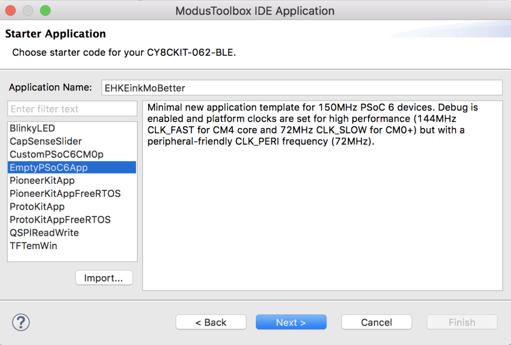
First, create a new project for the CY8CKIT-062-BLE
Then copy the “design.modus” from the previous project and paste it into the new project. You can do with ctrl-c and ctrl-v. Remember, the design.modus file is just an xml file that contains all of the configuration information for your project.
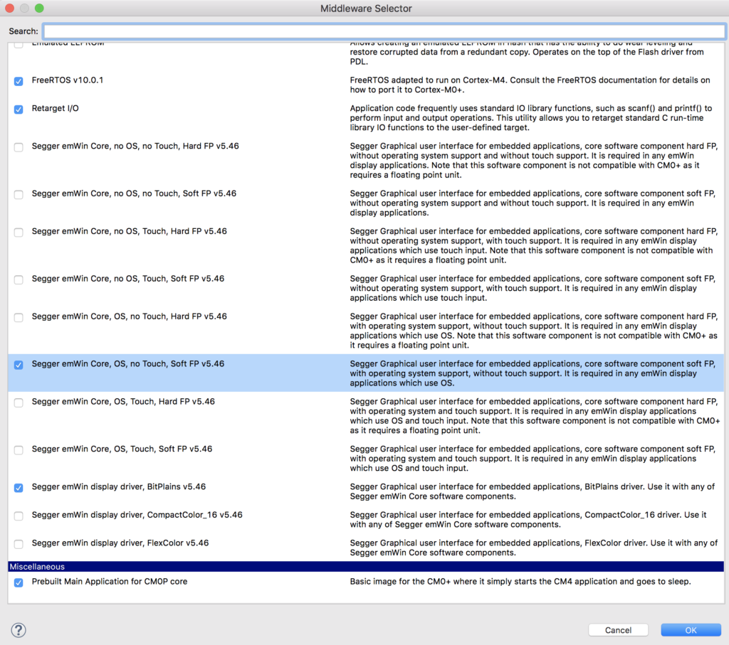
Next, select middleware for your project including FreeRTOS, Retarget I/O and the two Segger libraries.
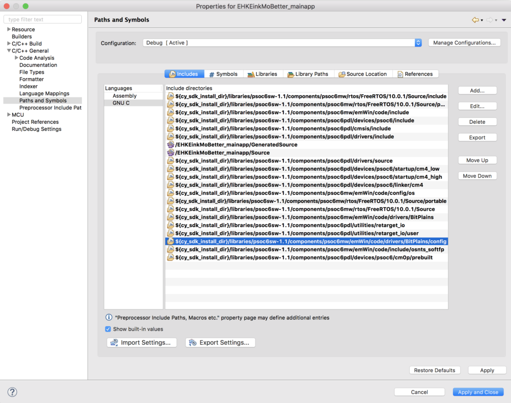
Recall from the previous article that you need to remove the incorrectly included path for …Bitplains/config. To do this right click on the project, select settings, pick paths and symbols then click on the wrong directory path and hit Delete.
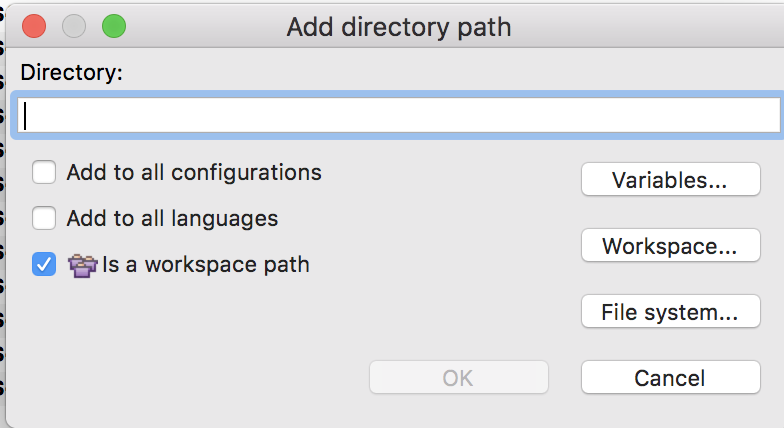
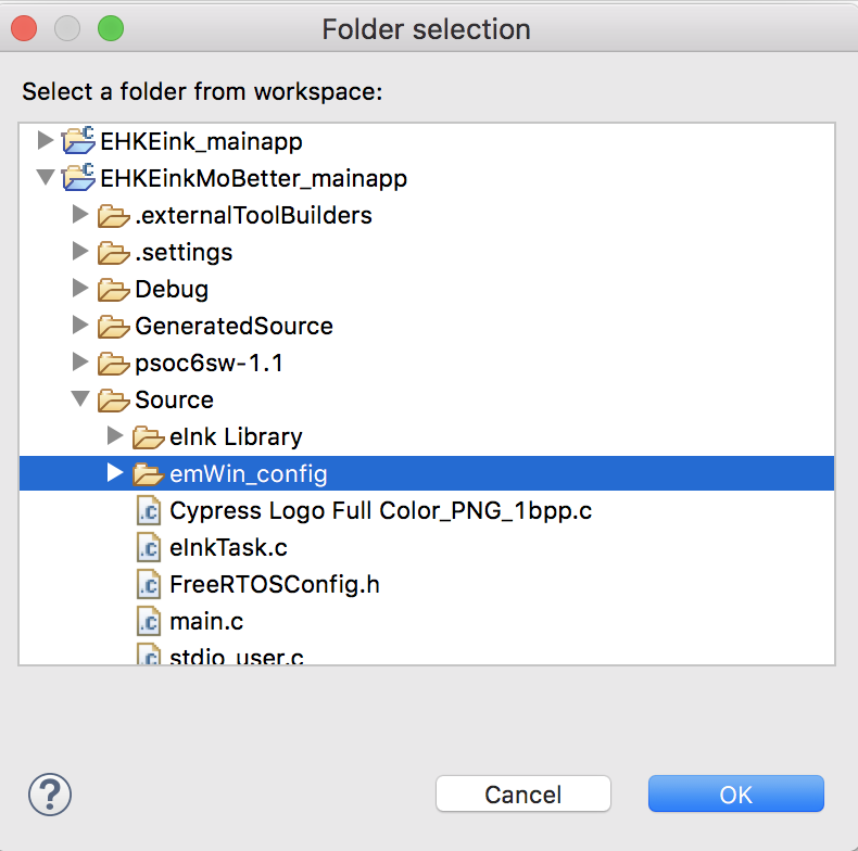
Now you need to add the paths for “eInk Library” and the “emWin_Config”. To do this click the “Add…” button. In the screen below you can see that I clicked “Is a workspace path” which will make it a relative path (i.e. not hardcoded). Now click “Workspace…”
Then select the “emWin_Config” folder
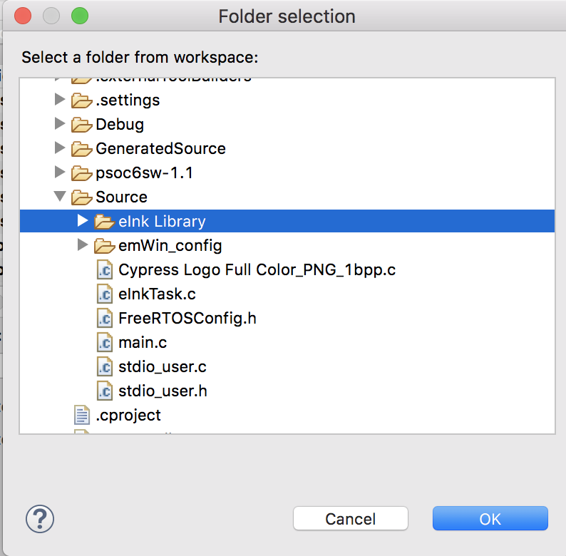
Then do the same process again for the eInk Library.
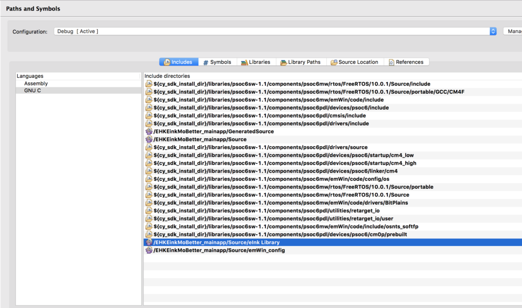
Now your Include path should look something like this:
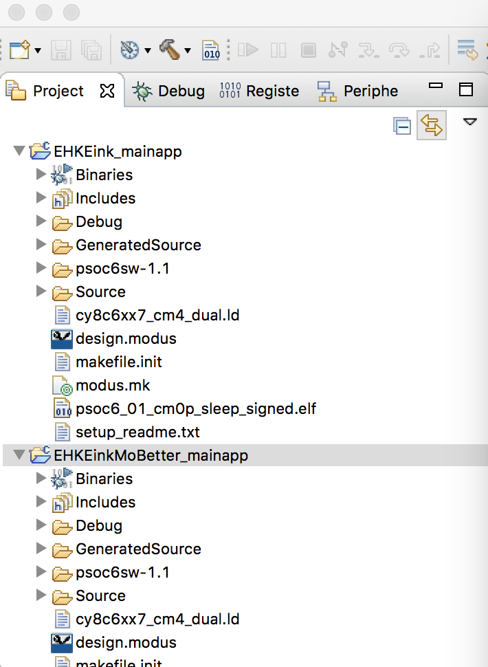
The next thing to do is copy your c and h files from the previous project. I just use ctrl-c and ctrl-v


Finally build it and make sure everything is working.
How does the clocking in the PSoC 6 work?
Before we can fix the SPI speed problem we should have a closer look at the PSoC 6 clocking system. Let’s start this by double clicking the design.modus in order to open up the device configurator. When you click on the “Platform” you should see a window that looks like this.
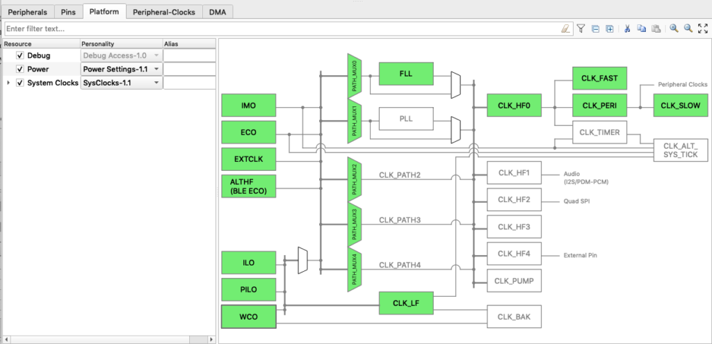
On the far left side of the picture you can see the “Input” section. These are reference sources that will drive all of the clock signals in the chip. This includes
- IMO – Internal Main Oscillator which is an 8Mhz 1% precision RC Oscillator (requires no external components)
- ECO – External Crystal Oscillator which will drive a precision crystal for a more accurate clock. This is sometimes called the “Megahertz clock”
- External Clock – a pin that will take a clock signal from outside the chip
- ILO – Internal Low Speed Oscillator – a 32Khz +- 30% (yes 30%) very low power very slow oscillator for generating wakeup signals etc.
- WCO – Watch Crystal Oscillator – a very precise circuit for driving a 32Khz watch crystal for very accurate clocks
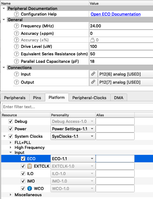
You can configure each of the “Input” clock sources on the “Input” section of the “System Clock”. In the picture below you can see that I have enabled all of the clock sources and I’m updating the parameters on the ECO. In the picture above all of the input sources that are enabled become green.
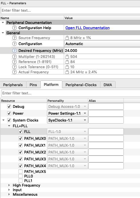
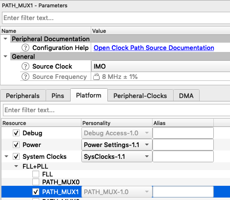
The next section of the clock tree is the “Paths”. On the input side of the paths are the “Sources” which are attached to six multiplexors labeled “PATH_MUXn”. You can use the “Paths” to select which Input source is driving the “Path” (i.e. IMO, ECO etc.). The outputs of the Paths are used to drive the HF_CLOCKs. The only trick in the paths is that “Path0” and “Path1” are special. In Path0 you can either use the Input to drive an FLL or you can just “pass through” the input signal to the output of the path. And in “Path1” you can either use the Input PATH_MUX1 to drive a PLL or as above, you can just “pass through” the input signal to the output of the path. Unfortunately this picture does not label “CLK_PATH0” or “CLK_PATH1”, but if they were on the picture, they would be just to the right of the three multiplexors just to the right of the FLL and PLL.
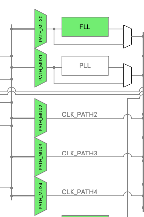
The next interesting section of the the paths is the FLL. The frequency locked loop can generate a higher frequency signal from a lower frequency input. In PSoC 6, the range of the FLL is 24 MHz to 100 MHz and is programmable by enabling the FLL with the checkbox, then setting the parameters. Notice that I set it for a 24 MHz clock.
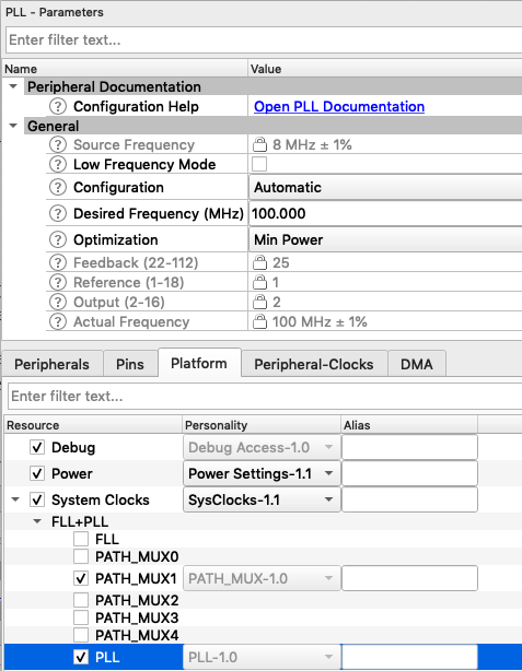
There is also a PLL in the chip. This can be configured to run between 12.5 MHz and 150 MHz with the IMO. If you select a different input source e.g. ECO you will have a different range of frequencies.
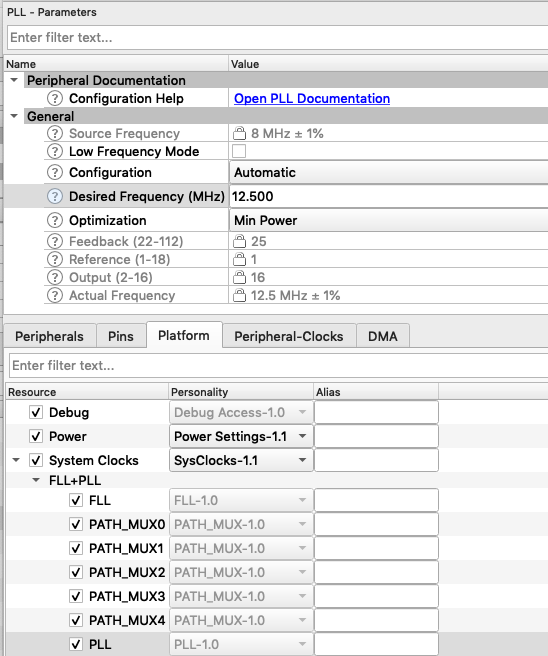
Notice that if you disable either the FLL or the PLL that the frequency of CLOCK_Path0 or CLOCK_Path1 will be set by the PATH_MUX0 or 1. In other words you can pick any of the input sources to drive into CLOCK_PATH0/1
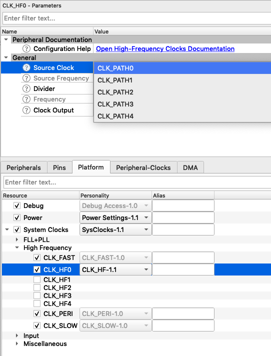
Just to the right of the “PATHs” there are five High Frequency Clocks labeled CLK_HF0 –> CLK_HF4. Each CLK HF has a multiplexor (which isnt shown) that selects its input from one of the 5 “paths”. It also has a divider that allows you to divide by 1,2,4,8. Here is a picture of the selector box for CLK_HF0
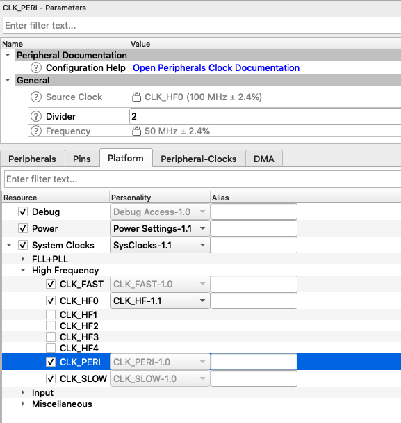
The last section of the clocks, that are relevant to this discussion, are “CLK_FAST” which sets the speed of the CPU (unfortunately the CPU clock isn’t shown on the picture… but it is attached to CLK_FAST) and “CLK_PERI” which is the source clock for many of the peripherals in the chip including the SCB/SPI and the SCB/UART. Each of those clocks also have a configuration box where you can select one more 8-bit divider. Notice that the source of CLK_FAST and CLK_PERI is always CLK_HF0. Here is a picture of the selection for CLK_PERI
Now that we know what’s going on with the clock tree, let’s fix the SPI speed.
Fix the SPI speed
You might recall that when I looked at the datasheet for the Pervasive EPD EInk display driver, that I found that the SPI can be run at 20MHz. Thats good. And you might also recall that the way that the code example project was configured had the speed set to 8.333MHz, that isn’t so good. These eInk screens take long enough to update as-is so speeding things up will make a better user experience.
We know that we want 20Mhz clock on the output of the SPI. And from the previous article we know that the input to the SPI must be a mutliple of the “oversample”. That means that we need the input clock to the SCB block to be 20,40,60,80,100,120, or 140 MHz. All right given all of that I think that I’m going to run my system with a base frequency of 100 MHz. So, fix the SPI to 20 MHz and 5 times oversampling.
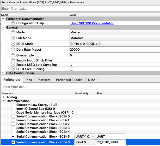
Somehow or the other in all of my clicking, I got PATH_MUX1 turned off. Ill turn it back on and select the IMO as the source.
Next Ill turn on the PLL and set it to 100 Mhz
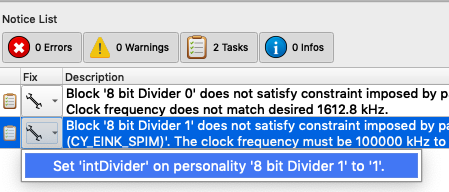
When I do this I get two errors, one for the UART and one for the SPI
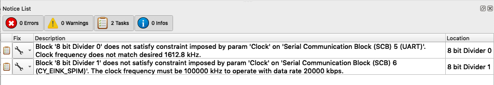
Let’s fix the SPI one first. To do that click on the little wrench and pick out the “8 bit diver 1 to 1”, which makes sense as we picked the oversampling to make that work.
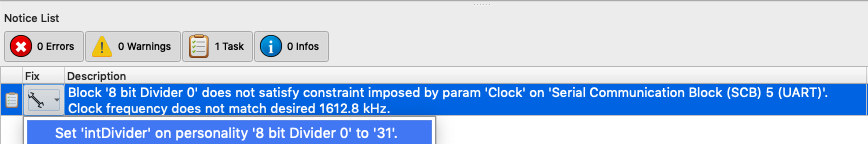
And then do the same thing to fix the UART
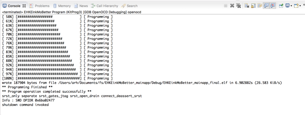
Build, Program and Test
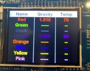
After all of that, build, program and test. On my development kit it is noticeably faster now. I suppose that I should figure out how to time it and see exactly what improvement I got, but Ill save that to the next Article.
In the next article Ill address the hardware timer.
No comment yet, add your voice below!