Summary
Recently, I have been helping a reader sort out some code that makes strings of WS2812 LEDs work. Specifically, this code takes data from a frame buffer inside of the PSoC 6 and drives it out a SPI port via the MOSI pin. I have written about this a couple of times, but, the new wrinkle in our code is that it allows you to use any combination of SPI port/pins on the chip. Instead of using the configurators to setup the SPI to GPIO connection, I setup the connection using PDL to talk directly to the PSoC 6 configuration the registers.
Perhaps it is obvious to everyone how a connection from a peripheral to a GPIO works, but I thought that I would write about it anyway. In this article I am going to show you a bunch of the documentation for PSoC as well as the PDL source code which implements the documentation. Specifically, I will show you the PSoC 6
Architecture TRM
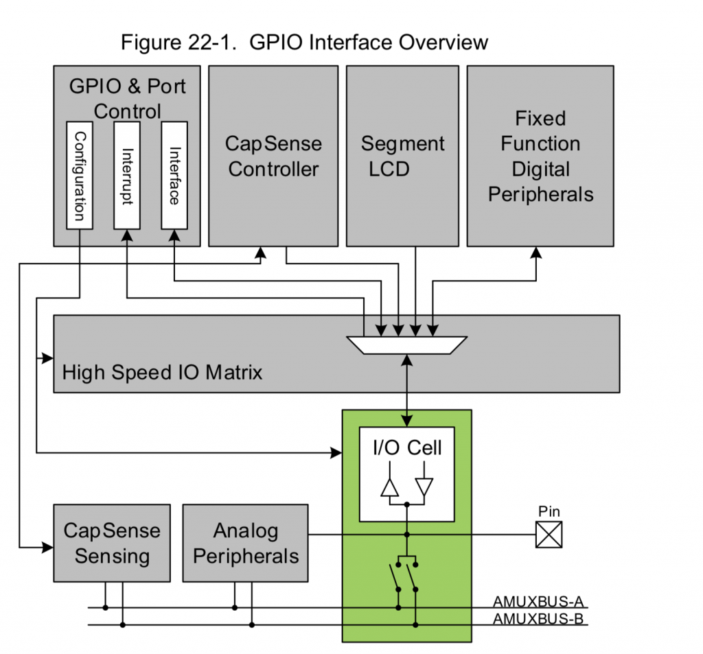
In the picture below, which I copied from the PSoC 6 Architecture TRM, you can see how an individual GPIO works. Starting at the Pin of the chip you can see that there are three connections from/to the pin (look at the green box).
- A set of switches to/from the Analog Mux Bus which enable CapSense or Analog peripherals to talk to the Pin
- A connection from the pin to the Analog peripherals (some Analog peripherals can attach directly to a pin and not though the Analog Mux Bus
- A connection to the High Speed I/O Matrix (HSIOM) – for the digital peripherals
Notice that all of the signals coming into the green box from the top are DIGITAL. All of the signals coming into the box from the bottom are Analog and the line coming into the middle of the box controls the behavior of the I/O.
For my case the SPI is one of the “Fixed Function Digital Peripherals”. In order to get it to connect to the pin I will beed to pick out the right signal in the multiplexer that is in the HSIOM Matrix box.
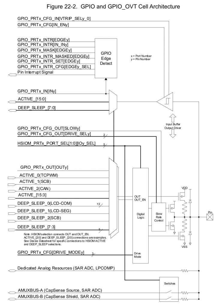
When you scroll down a little bit further in the Architecture TRM, the next diagram is a more detailed description of the GPIO. Notice that there are a bunch of configuration register bits which setup different parts of the I/O like slew rate, interrupts, drive mode etc. Notice that the multiplexer that is connected to “out”
and “out_en” has a bunch of different possible signals. Including “GPIO_PRTx_OUT[OUTy]” which is a register bit which is can be used for “digital write”. For instance GPIO_PRT0_OUT[2] would be P0_2. The other interesting thing going on here is you can see that there are really three classes of signals attached to the mutiplexer
- The digital output pin
- Active signals – which work while the chip is not in deep sleep
- Deep Sleep signals – which work while the chip is in deep sleep.
On the output side you can see the two pullup and pulldown resistors, as well as the two transistors which pullup and pull down. All of these can be configured to be connected… or not.
And finally at the bottom of the I/O you can see the analog signals.
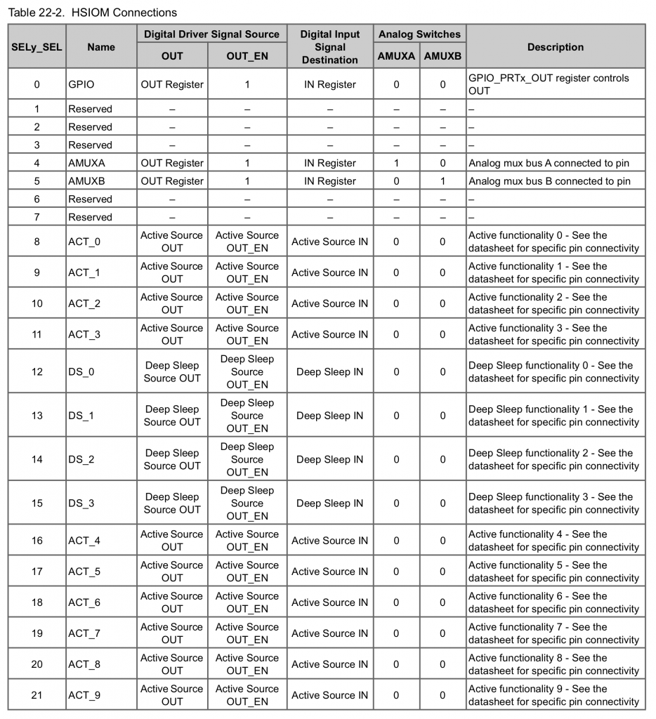
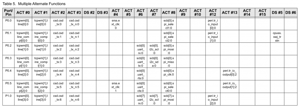
If you look a little bit further down in the Architecture TRM you will find this table which describes how each of the actual pins on the multiplexer work.
PSoC 6 Register TRM
If you want to start to make specific configurations for specific pins you will need to look into the PSoC 6 Register TRM. In that document you will find that the
Register TRM
Register TRM
PSoC 6 Datasheet
But what are all of the active and deep sleep signals? Well if you look in the PSoC 6 data sheet you can find all of those connections. For instance on P0.1 active signal 8 is the SCB 0 SPI Select signal 2.
PSoC 6 PDL
But really all of these register reads and writes are not really that fun. So, Cypress provides other, less painful ways of getting things going. Specifically,
- void Cy_GPIO_SetHSIOM(GPIO_PRT_Type* base, uint32_t pinNum, en_hsiom_sel_t value)
or
- Cy_GPIO_Pin_Init(GPIO_PRT_Type *base, uint32_t pinNum, const cy_stc_gpio_pin_config_t *config)
When you call both of these function you need to provide the value for the multipler either directly in the Cy_GPIO_SetHSIOM or indirectly in the Cy_GPIO_Pin_Init case where you provide it as a member of the cy_stc_gpio_pin_config_t *config structure called “hsiom”
Depending on which package you have selected you will have a file like gpio_psoc6_01_124_bga.h which will have both the generic definitions for the HSIOM multiplexer select (like this)
/* HSIOM Connections */
typedef enum
{
    /* Generic HSIOM connections */
    HSIOM_SEL_GPIO                  =  0,       /* GPIO controls 'out' */
    HSIOM_SEL_GPIO_DSI              =  1,       /* GPIO controls 'out', DSI controls 'output enable' */
    HSIOM_SEL_DSI_DSI               =  2,       /* DSI controls 'out' and 'output enable' */
    HSIOM_SEL_DSI_GPIO              =  3,       /* DSI controls 'out', GPIO controls 'output enable' */
    HSIOM_SEL_AMUXA                 =  4,       /* Analog mux bus A */
    HSIOM_SEL_AMUXB                 =  5,       /* Analog mux bus B */
    HSIOM_SEL_AMUXA_DSI             =  6,       /* Analog mux bus A, DSI control */
    HSIOM_SEL_AMUXB_DSI             =  7,       /* Analog mux bus B, DSI control */
    HSIOM_SEL_ACT_0                 =  8,       /* Active functionality 0 */
    HSIOM_SEL_ACT_1                 =  9,       /* Active functionality 1 */
    HSIOM_SEL_ACT_2                 = 10,       /* Active functionality 2 */
    HSIOM_SEL_ACT_3                 = 11,       /* Active functionality 3 */
    HSIOM_SEL_DS_0                  = 12,       /* DeepSleep functionality 0 */
    HSIOM_SEL_DS_1                  = 13,       /* DeepSleep functionality 1 */
    HSIOM_SEL_DS_2                  = 14,       /* DeepSleep functionality 2 */
    HSIOM_SEL_DS_3                  = 15,       /* DeepSleep functionality 3 */
    HSIOM_SEL_ACT_4                 = 16,       /* Active functionality 4 */
    HSIOM_SEL_ACT_5                 = 17,       /* Active functionality 5 */
    HSIOM_SEL_ACT_6                 = 18,       /* Active functionality 6 */
    HSIOM_SEL_ACT_7                 = 19,       /* Active functionality 7 */
    HSIOM_SEL_ACT_8                 = 20,       /* Active functionality 8 */
    HSIOM_SEL_ACT_9                 = 21,       /* Active functionality 9 */
    HSIOM_SEL_ACT_10                = 22,       /* Active functionality 10 */
    HSIOM_SEL_ACT_11                = 23,       /* Active functionality 11 */
    HSIOM_SEL_ACT_12                = 24,       /* Active functionality 12 */
    HSIOM_SEL_ACT_13                = 25,       /* Active functionality 13 */
    HSIOM_SEL_ACT_14                = 26,       /* Active functionality 14 */
    HSIOM_SEL_ACT_15                = 27,       /* Active functionality 15 */
    HSIOM_SEL_DS_4                  = 28,       /* DeepSleep functionality 4 */
    HSIOM_SEL_DS_5                  = 29,       /* DeepSleep functionality 5 */
    HSIOM_SEL_DS_6                  = 30,       /* DeepSleep functionality 6 */
    HSIOM_SEL_DS_7                  = 31,       /* DeepSleep functionality 7 */
As well as the pin by pin definitions… like this for P0_2
    /* P0.2 */
    P0_2_GPIO                       =  0,       /* GPIO controls 'out' */
    P0_2_AMUXA                      =  4,       /* Analog mux bus A */
    P0_2_AMUXB                      =  5,       /* Analog mux bus B */
    P0_2_AMUXA_DSI                  =  6,       /* Analog mux bus A, DSI control */
    P0_2_AMUXB_DSI                  =  7,       /* Analog mux bus B, DSI control */
    P0_2_TCPWM0_LINE1               =  8,       /* Digital Active - tcpwm[0].line[1]:0 */
    P0_2_TCPWM1_LINE1               =  9,       /* Digital Active - tcpwm[1].line[1]:0 */
    P0_2_CSD_CSD_TX                 = 10,       /* Digital Active - csd.csd_tx:2 */
    P0_2_CSD_CSD_TX_N               = 11,       /* Digital Active - csd.csd_tx_n:2 */
    P0_2_LCD_COM2                   = 12,       /* Digital Deep Sleep - lcd.com[2]:0 */
    P0_2_LCD_SEG2                   = 13,       /* Digital Deep Sleep - lcd.seg[2]:0 */
    P0_2_SCB0_UART_RX               = 18,       /* Digital Active - scb[0].uart_rx:0 */
    P0_2_SCB0_I2C_SCL               = 19,       /* Digital Active - scb[0].i2c_scl:0 */
    P0_2_SCB0_SPI_MOSI              = 20,       /* Digital Active - scb[0].spi_mosi:0 */
If you look at the Cy_GPIO_Pin_Init function you will see that on line 96 it sets the register which picks the correct pin mux.
cy_en_gpio_status_t Cy_GPIO_Pin_Init(GPIO_PRT_Type *base, uint32_t pinNum, const cy_stc_gpio_pin_config_t *config)
{
    cy_en_gpio_status_t status = CY_GPIO_BAD_PARAM;

    if ((NULL != base) && (NULL != config))
    {
        uint32_t maskCfgOut;
        uint32_t tempReg;

        CY_ASSERT_L2(CY_GPIO_IS_PIN_VALID(pinNum));
        CY_ASSERT_L2(CY_GPIO_IS_VALUE_VALID(config->outVal));
        CY_ASSERT_L2(CY_GPIO_IS_DM_VALID(config->driveMode));
        CY_ASSERT_L2(CY_GPIO_IS_HSIOM_VALID(config->hsiom));
        CY_ASSERT_L2(CY_GPIO_IS_INT_EDGE_VALID(config->intEdge));
        CY_ASSERT_L2(CY_GPIO_IS_VALUE_VALID(config->intMask));
        CY_ASSERT_L2(CY_GPIO_IS_VALUE_VALID(config->vtrip));
        CY_ASSERT_L2(CY_GPIO_IS_VALUE_VALID(config->slewRate));
        CY_ASSERT_L2(CY_GPIO_IS_DRIVE_SEL_VALID(config->driveSel));
        CY_ASSERT_L2(CY_GPIO_IS_VALUE_VALID(config->vregEn));
        CY_ASSERT_L2(CY_GPIO_IS_VALUE_VALID(config->ibufMode));
        CY_ASSERT_L2(CY_GPIO_IS_VALUE_VALID(config->vtripSel));
        CY_ASSERT_L2(CY_GPIO_IS_VREF_SEL_VALID(config->vrefSel));
        CY_ASSERT_L2(CY_GPIO_IS_VOH_SEL_VALID(config->vohSel));

        Cy_GPIO_Write(base, pinNum, config->outVal);
        Cy_GPIO_SetDrivemode(base, pinNum, config->driveMode);
        Cy_GPIO_SetHSIOM(base, pinNum, config->hsiom);

        Cy_GPIO_SetInterruptEdge(base, pinNum, config->intEdge);
        Cy_GPIO_SetInterruptMask(base, pinNum, config->intMask);
        Cy_GPIO_SetVtrip(base, pinNum, config->vtrip);

        /* Slew rate and Driver strength */
        maskCfgOut = (CY_GPIO_CFG_OUT_SLOW_MASK << pinNum)
                     | (CY_GPIO_CFG_OUT_DRIVE_SEL_MASK << ((uint32_t)(pinNum << 1U) + CY_GPIO_CFG_OUT_DRIVE_OFFSET));
        tempReg = GPIO_PRT_CFG_OUT(base) & ~(maskCfgOut);

        GPIO_PRT_CFG_OUT(base) = tempReg | ((config->slewRate & CY_GPIO_CFG_OUT_SLOW_MASK) << pinNum)
                            | ((config->driveSel & CY_GPIO_CFG_OUT_DRIVE_SEL_MASK) << ((uint32_t)(pinNum << 1U) + CY_GPIO_CFG_OUT_DRIVE_OFFSET));

        /* SIO specific configuration */
        tempReg = GPIO_PRT_CFG_SIO(base) & ~(CY_GPIO_SIO_PIN_MASK);
        GPIO_PRT_CFG_SIO(base) = tempReg | (((config->vregEn & CY_GPIO_VREG_EN_MASK)
                                         | ((config->ibufMode & CY_GPIO_IBUF_MASK) << CY_GPIO_IBUF_SHIFT)
                                         | ((config->vtripSel & CY_GPIO_VTRIP_SEL_MASK) << CY_GPIO_VTRIP_SEL_SHIFT)
                                         | ((config->vrefSel & CY_GPIO_VREF_SEL_MASK)  << CY_GPIO_VREF_SEL_SHIFT)
                                         | ((config->vohSel & CY_GPIO_VOH_SEL_MASK) << CY_GPIO_VOH_SEL_SHIFT))
                                           << ((pinNum & CY_GPIO_SIO_ODD_PIN_MASK) << CY_GPIO_CFG_SIO_OFFSET));

        status = CY_GPIO_SUCCESS;
    }

    return(status);
}
And finally the Cy_GPIO_SetHSIOM actually writes to the register.
__STATIC_INLINE void Cy_GPIO_SetHSIOM(GPIO_PRT_Type* base, uint32_t pinNum, en_hsiom_sel_t value)
{
    uint32_t portNum;
    uint32_t tempReg;
    HSIOM_PRT_V1_Type* portAddrHSIOM;

    CY_ASSERT_L2(CY_GPIO_IS_PIN_VALID(pinNum));
    CY_ASSERT_L2(CY_GPIO_IS_HSIOM_VALID(value));

    portNum = ((uint32_t)(base) - CY_GPIO_BASE) / GPIO_PRT_SECTION_SIZE;
    portAddrHSIOM = (HSIOM_PRT_V1_Type*)(CY_HSIOM_BASE + (HSIOM_PRT_SECTION_SIZE * portNum));

    if(pinNum < CY_GPIO_PRT_HALF)
    {
        tempReg = HSIOM_PRT_PORT_SEL0(portAddrHSIOM) & ~(CY_GPIO_HSIOM_MASK << (pinNum << CY_GPIO_HSIOM_OFFSET));
        HSIOM_PRT_PORT_SEL0(portAddrHSIOM) = tempReg | ((value & CY_GPIO_HSIOM_MASK) << (pinNum << CY_GPIO_HSIOM_OFFSET));
    }
    else
    {
        pinNum -= CY_GPIO_PRT_HALF;
        tempReg = HSIOM_PRT_PORT_SEL1(portAddrHSIOM) & ~(CY_GPIO_HSIOM_MASK << (pinNum << CY_GPIO_HSIOM_OFFSET));
        HSIOM_PRT_PORT_SEL1(portAddrHSIOM) = tempReg | ((value & CY_GPIO_HSIOM_MASK) << (pinNum << CY_GPIO_HSIOM_OFFSET));
    }
}
PSoC 6 SPI
Finally, it may seem obvious, but there is a limited set of connections to each GPIO in PSoC 6. This means that any given SCB can only connect its SPI pins to a specific set of pins on the chip. But, what are they? You can either look at the data sheet, or you can search the file which you will find the pin definitions which will all be in the form of Px_y_SCBz_SPI_MOSI and this will give you a complete map.
No comment yet, add your voice below!