Summary
Last week while working on a PSoC FreeRTOS Project, I looked at the CY8CKIT-044 Development kit that I was using and remembered that right under the Ambient Light Sensor there is a Cypress FM24V10 FRAM. Way back, I started pushing our Development Kit team to put other Cypress parts onto the dev kits…. and because they are awesome, they aggressively started doing that. One of those chips is the FM24V10 FRAM. As I looked at the chip, I realized again that I had never really written anything into the FM24V10 FRAM on any of our dev kits, which seems silly after I pushed the dev kit team for them. I realized that the reason I had never used the FM24V10 FRAM was I didn’t have a nifty way to write files. But, while working on the other FreeRTOS projects, I noticed the FreeRTOS FAT SL Filesystem is built into FreeRTOS. The next couple (3?) articles I will talk about making the FreeRTOS FAT SL Filesystem work on a PSoC4200M with a FM24V10 I2C FRAM.
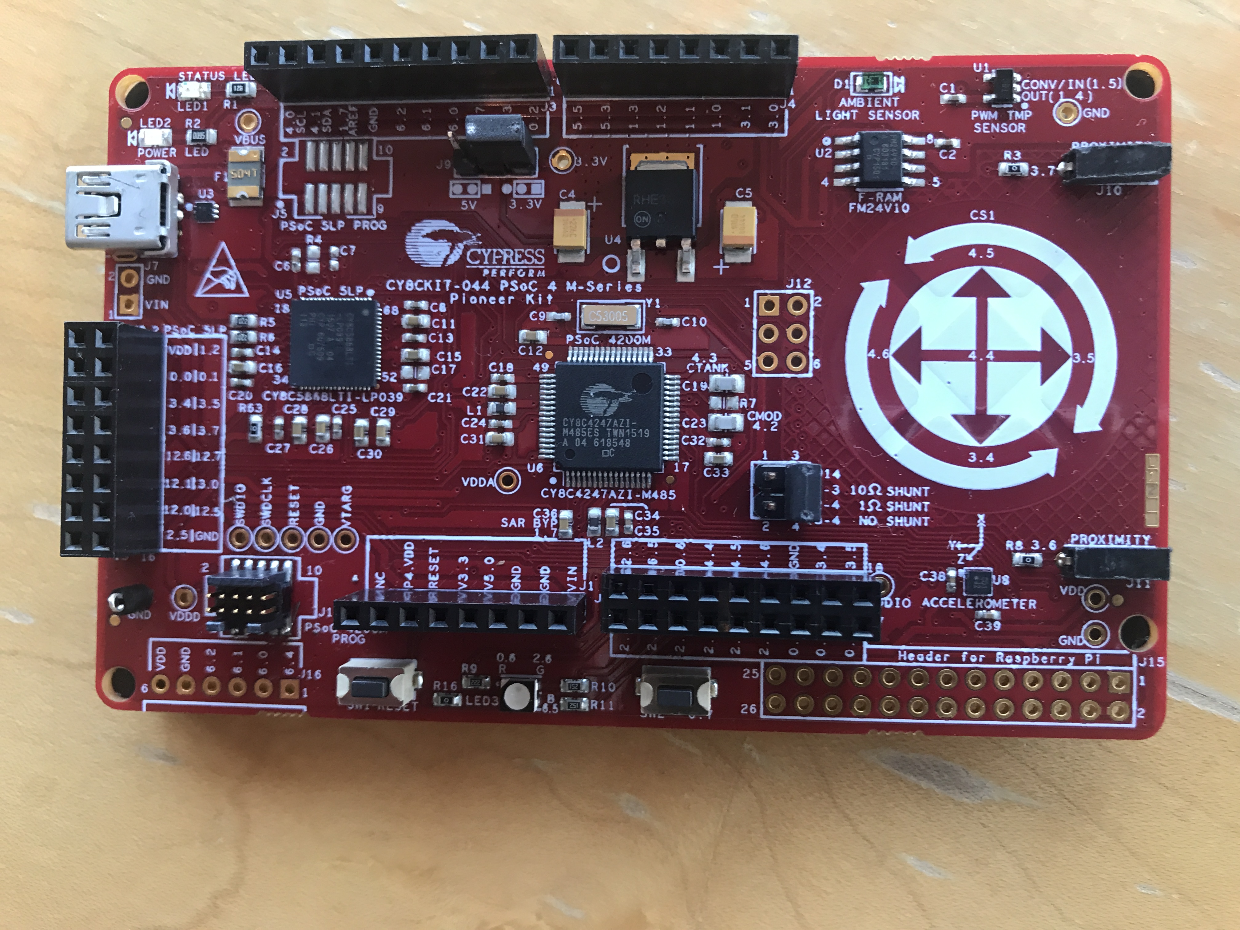
The Cypress FM24V10 FRAM
The “F” in FRAM stands for ferroelectric. What that means is each of the memory cells is a little magnet. So what you say? Well the “what” is that FRAMs don’t wear out (unlike Flash), you can write individual cells (unlike Flash), and it is super low power, it is plenty fast (I2C = 3.4MBS), and it retains data for a long long time (151 years).
That list sounds great. Actually really great. But, what is the but? There are two answers to that question. The first answer is there is a density penalty, the biggest I2C FRAM is 1Mb where you can buy a 1Gb NOR Flash or even bigger NAND Flash. The next issue is price. The digikey pricing for a 128Kb FRAM is $12.76 or 9.9c/kb and a 1GB NOR Flash is $14.97 or 0.0014c/kb. That means an FRAM is 6724 x as expensive per bit.
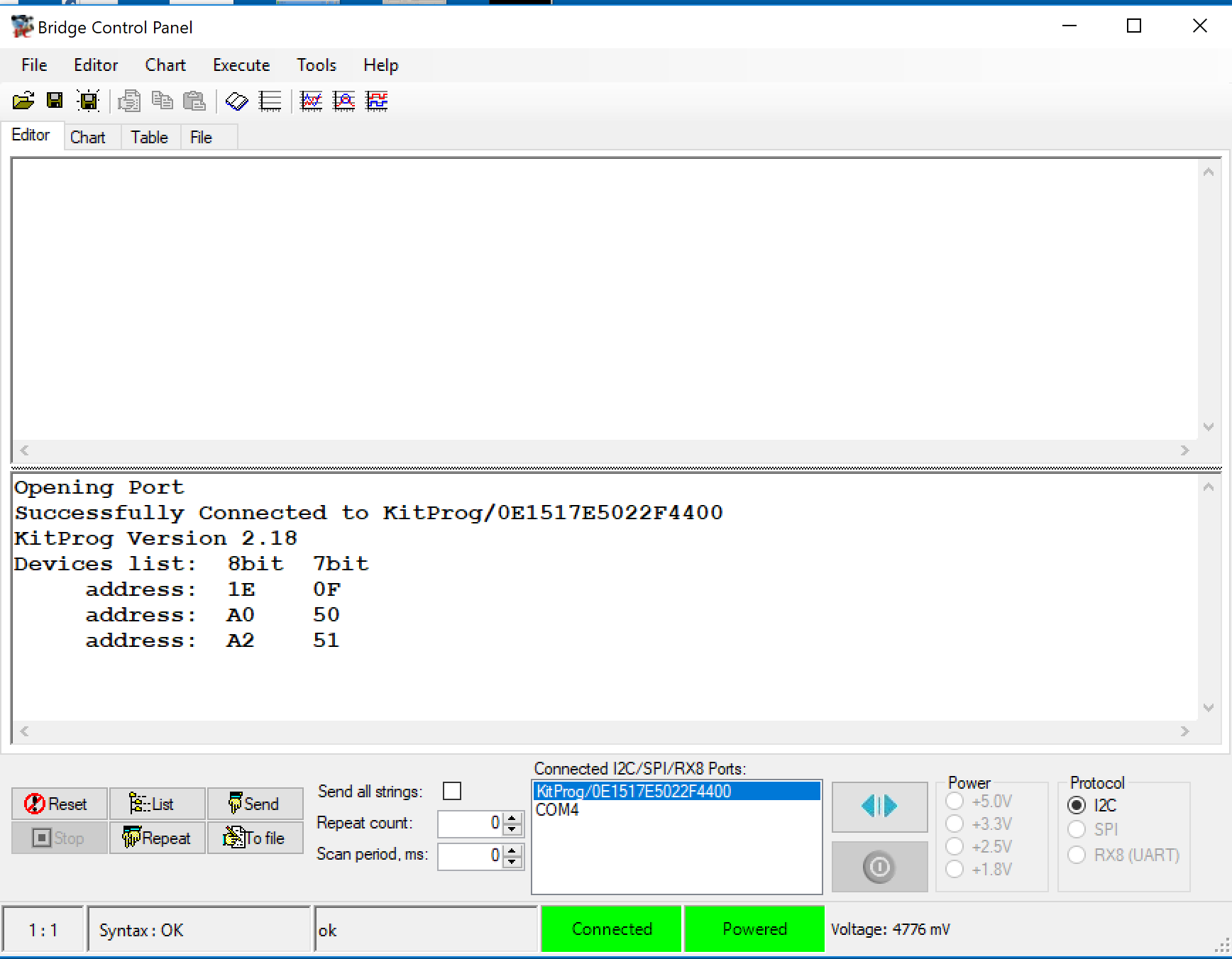
How do I use it? The FRAM is attached to the I2C pins on the CY8CKIT-044. That means that I can talk to it with either the Bridge Control Panel, or with the PSoC. To start with I will show you the Bridge Control Panel. First, I probe the I2C bus, and I see that there are three I2C devices.
- 0x0F = The I2C Accelerometer (which I wrote about here)
- 0x50= The first 64K of FRAM
- 0x51 = The second 64K of FRAM
The 128K FRAM is divided into two banks which are accessed on separate I2C addresses. By splitting 128K into two blocks of 64K the chip designers optimized the addressing of the memory. In order to access 64K you need 16-bits, which means to access 128K you need 17-bits. This would have required sending a whole extra byte of address when you really only needed 1 of those 8 bits. They avoid this problem by having two addresses.
The FM24V10 FRAM is easy to use as it implements an EzI2C (like) protocol. EZI2C keeps an internal address pointer. The pointer is automatically incremented each time you do an I2C transaction. When you do a write transaction, the first two bytes you write are placed into the address pointer. I say “EZI2C like” because the pointer is not retained between transactions. Some examples:
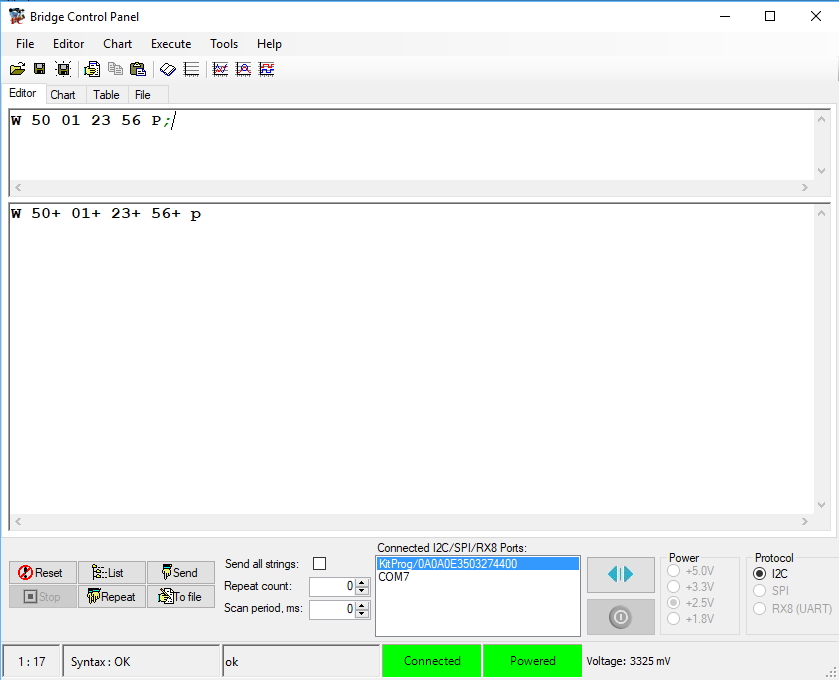
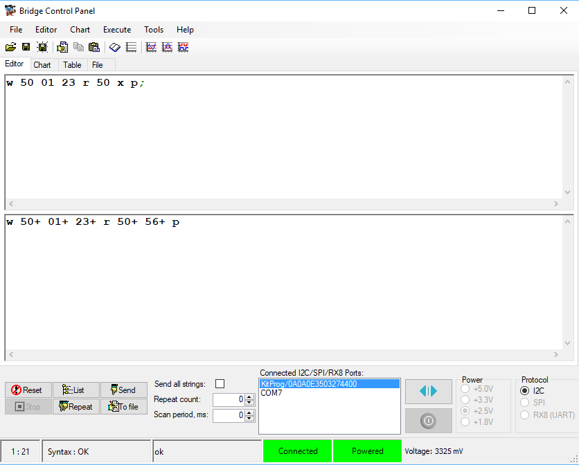
If I want to write 0x56 into location 0x0123 I would issue
- I2C Start
- I2C Write to I2C address 0x50
- Send 0x01, 0x02 (which write the address pointer)
- Send 0x56
- I2C Stop
I can do that sequence with the Bridge Control Panel command “W 50 01 23 56 P;” The “W” stands for “send a start and send the 7-bit address 0x50 (left shifted 1) and send a ‘0’ for write”. For some reason the engineers at Philips decided that the I2C protocol would have 7-bit addressing and then 1 bit to represent write or read. When you talk about I2C there is always confusion about “8-bit address” versus “7-bit address”. When they talk about 8-bit address they are talking about the 7-bit address shifted left 1 bit and then or-ed with the read or write bit. Here is a picture from the bridge control panel:
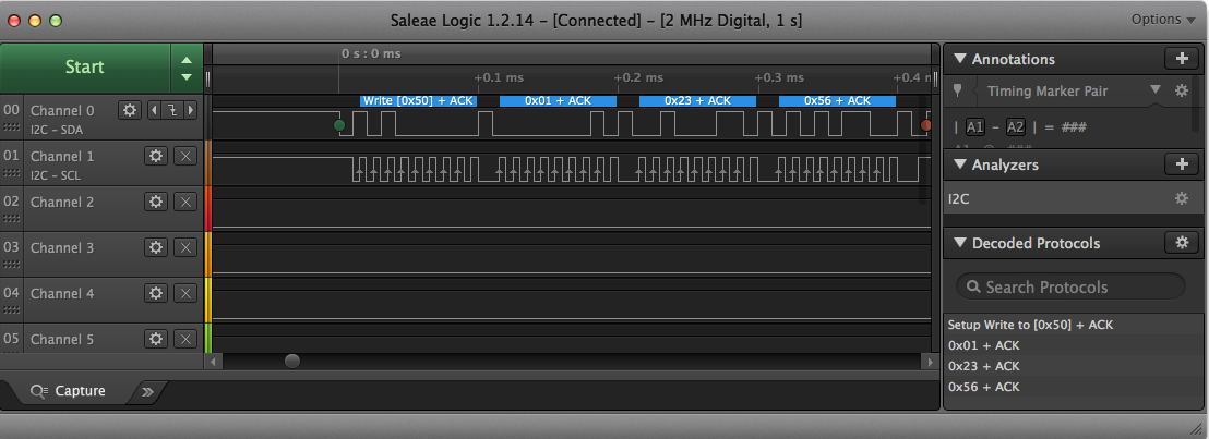
And the same thing from the logic analyzer.
Once I have written 0x56 into address 0x0123, I can read it back by a “w 50 01 23 r 50 x p;” which sends:
- I2C Start
- I2C Write to I2C address 0x50
- Send 0x01, 0x02 (which write the address pointer)
- I2C Restart
- Sends 0x50 (shifted left) or-ed with “read”
- Reads the byte
- I2C Stop
In the transaction output window below, you can see that the “x” is replaced with “56” meaning that it read the previously written value back.
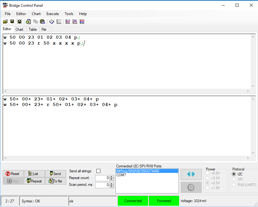
The only other interesting thing about the protocol is that once you have sent and address, you can keep reading, or writing without sending the address again. For instance to write 01, 02, 03, 04 to address 23, 23,25 and 26 you can send “W 50 00 23 01 02 03 04 p”, then you can read it back with “W 50 00 23 r 50 x x x x p;”
In the next Article I will start the process of using the Free RTOS File System to write and read from the I2C FRAM.
No comment yet, add your voice below!