Summary
Last week I got a question from a customer about how to write into the PSoC 4 Flash. I sent him a fairly straight forward email message explaining the process in English… but after reflecting a little bit, I decided to write an example project as “C’ is often much clearer. And yes I know that this article it doesn’t have much to do with IoT, but hopefully it is helpful to someone. In this article I will explain:
- The organization of the PSoC 4 Flash
- The risks and issues of writing to the PSoC 4 Flash
- A program that demonstrates reading and writing the PSoC 4 Flash
- How to protect rows of the PSoC 4 Flash
Organization of the PSoC 4 Flash
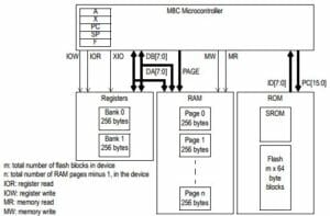
The PSoC 4 Flash is organized into an array that starts at memory address 0x00 and has 128 byte rows. Different versions of the chip will have different numbers of rows and possibly two arrays (in the case of PSoC 4 BLE II). The exact configuration of your part is knowable in the firmware by a set of #defines that are built for you by PSoC Creator. Here is a snapshot from the PSoC 4 System Reference Guide Chapter 8.
You can use that information along with the System call CySysFlashWriteRow() to write into the flash of your device.
Risks and Issues Writing the PSoC 4 Flash
There are several risks that you must take into account when performing a PSoC 4 Flash write (or for that matter writing Flash in any other MCU).
- You must write a complete row at a time. In PSoC 4 that is 128 bytes. So, even if you want to write only 1 byte, you will need to read in all of the data surrounding that byte in the row and make sure you don’t overwrite something important.
- You can easily write someplace bad and brick your part (e.g. if you overwrite your program, or exception vectors, or …). You need to be very careful that you are writing in the correct place
- It takes 20ms, which is a long time in the context of MCU speed, to write a row of flash and the MCU comes to a standstill while that is happening (all of the interrupts are off etc.)
- The Flash will eventually wear out. If you look at the data sheet for PSoC 4 you will find that the endurance of the Flash is 100K writes. If you are continually updating a place in the memory, you will eventually wear it out
A PSoC 4 Flash Write Demo Project
To demonstrate the process of a PSoC 4 Flash write I created a project that:
- Initializes a 128 byte array in the Flash (aligned to a complete row) with 0’s
- Lets you read the Flash array into a RAM array by pressing a key on the keyboard
- Lets you printout the values of the Flash array
- Lets you printout the values of the RAM array
- Lets you increment the values of the RAM array
- Lets you write the RAM array into the Flash
Normally when you declare a variable in C it will be assigned to the RAM somewhere (either on the Stack or in the Data or BSS section of the RAM). In order to have my array be assigned to the Flash, I declare the array to be “const”. The first time I did this I did not include the “={0}” in the declaration, and the compiler decided to put the array in the RAM, but when I initialized one of the elements it assigned it to the Flash. The CY_ALIGN() macro tells the linker to put the start of the “row” array on a 128 byte boundary. In other words completely aligning to a Flash row.
// Allocate 1 row of flash... make it aligned to the row size
// and initializde it with 0's
// the const keeps it in the flash (not in the data segment)
const uint8_t row[CY_FLASH_SIZEOF_ROW] CY_ALIGN(CY_FLASH_SIZEOF_ROW) = {0};
At the start of main, I declare array called “data” which will reside in the RAM. I will use this array as a buffer to read Flash data into, then change it, then write it back to the Flash.
We know that the Flash is arranged in rows of 128 bytes (well, actually rows of size CY_FLASH_SIZEOF_ROW). To calculate the row number of the my array “row”, I use the Address of the row divided by the row size. (the CY_FLASH_BASE is 0x00 because the Flash starts at Address 0x00)
    uint8_t data[CY_FLASH_SIZEOF_ROW];
    int rowNum;
    // calculate which row in the flash that the "row" array resides
    rowNum = ((int)row - CY_FLASH_BASE) / CY_FLASH_SIZEOF_ROW;
To make things a bit easier I create a function called “dump” which just prints the values of a “size “of memory in hex format. The function just takes an address that you want to start dumping to the screen.
// This function dumps a block of memory into rows of hex ...16 bytes long in hex
void dump(uint8_t *array, int size)
{
    int i,j;
    j=0;
    for(i=0;i<size;i++)
    {
        dbgprintf("%2X ",array[i]);
        j=j+1;
        if(j==16) // 16 values per line
        {
            j = 0;
            dbgprintf("\n");
        }
    }
    UART_UartPutString("\n");
}
In order to test this whole thing I use a UART to read from the keyboard and display to the screen. The main function is just a loop that reads keys and then does a big “switch”.
When you press ‘f’ it dumps the Flash “row”
When you press ‘r’ it copies the Flash “row” into the array “data” (which resides in the RAM)
When you press ‘i’ it increments the values in the “data” array
When you press “R” it dumps out the values in the “data” array
When you press ‘q’ it prints out information about the rowNumber, row size etc.
   for(;;)
    {
        char c;
        c = UART_UartGetChar();
        switch(c)
        {
            case 'f':
                UART_UartPutString("Dumping Flash\n");
                dump((uint8_t *)row,CY_FLASH_SIZEOF_ROW);
                break;
            case 'r':
                UART_UartPutString("Reading Flash into RAM\n");
                memcpy(data,row,(int)CY_FLASH_SIZEOF_ROW);
            break;

            case 'i':
                UART_UartPutString("Incrementing RAM Array\n");
                data[0] = data[0] + 1;
                for(i=1;i<(int)CY_FLASH_SIZEOF_ROW;i++)
                {
                    data[i] = data[i-1]+1;
                }
            break;
            case 'R':
                dbgprintf("Dumping RAM Array\n");
                dump(data,CY_FLASH_SIZEOF_ROW);
            break;

            case 'q':
                dbgprintf("Row Number = %d\n",rowNum);
                dbgprintf("RowSize = %d\n",CY_FLASH_SIZEOF_ROW);
                dbgprintf("Flash Address = %X\n",CY_FLASH_BASE);
                dbgprintf("Row Address = %X\n",(unsigned int)row);
                dbgprintf("Data Address = %X\n",(unsigned int)data);

            break;
When you press ‘w’, it writes the “data” array into the “row” array in the Flash using the “CySysFlashWriteRow()” system call
            case 'w':
                dbgprintf("Writing Flash from RAM Buffer\n");
                rval = CySysFlashWriteRow(rowNum,data);
                if(rval == CY_SYS_FLASH_SUCCESS )
                {
                    dbgprintf("Flash Write Sucess\n");
                }
                else if (rval == CY_SYS_FLASH_INVALID_ADDR)
                {
                    dbgprintf("Flash Write Failed: Invalid Address\n");
                }
                else if (rval == CY_SYS_FLASH_PROTECTED)
                {
                    dbgprintf("Flash Write Failed: Flash Protected\n");
                }
                else {
                    dbgprintf("Flash Write Failed: Unknown\n");
                }
            break;
Testing the Program
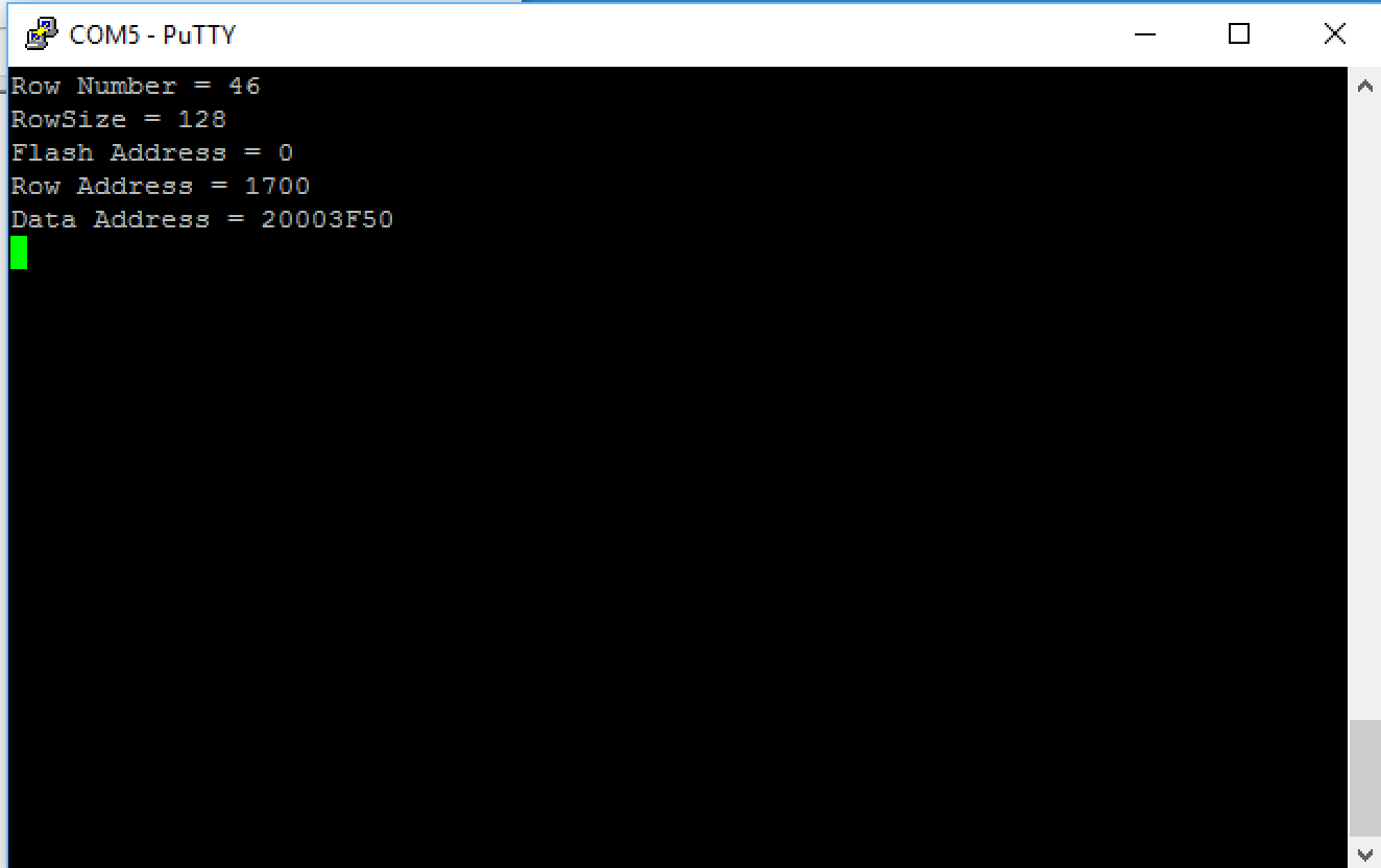
After I program the device, I first press “q” to find out the information about the PSoC 4 Flash array. You can see that my “row” is the 46th row in the Flash and resides at address 0x1700 (as I type this I wish that I hadn’t mixed decimal and hex … and that I had called my “row” variable something other than “row”). You can also see that the rows are 128 bytes and that the Flash array starts at address 0x0. All that is good.
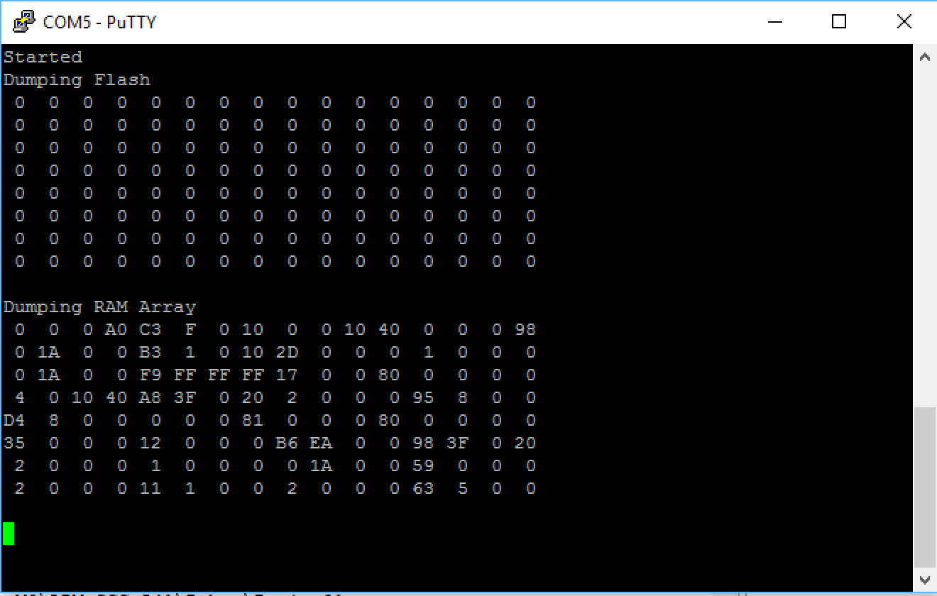
When I press ‘f’ to dump out the Flash array, you can see that my row has all 0’s in it. Then I press ‘R’ to dump out my RAM array and you can see that it has garbly-gook in it (which makes sense as I didn’t initialize the array)
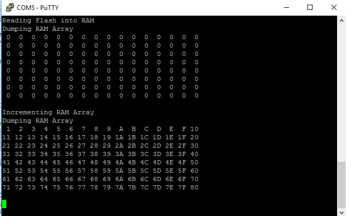
Next, I press ‘r’ to copy the PSoC 4 Flash array into the RAM buffer. Then I press “i” to increment the values in the RAM array, then I dump it out. Lastly, I press ‘w’ to write it to the PSoC 4 Flash.
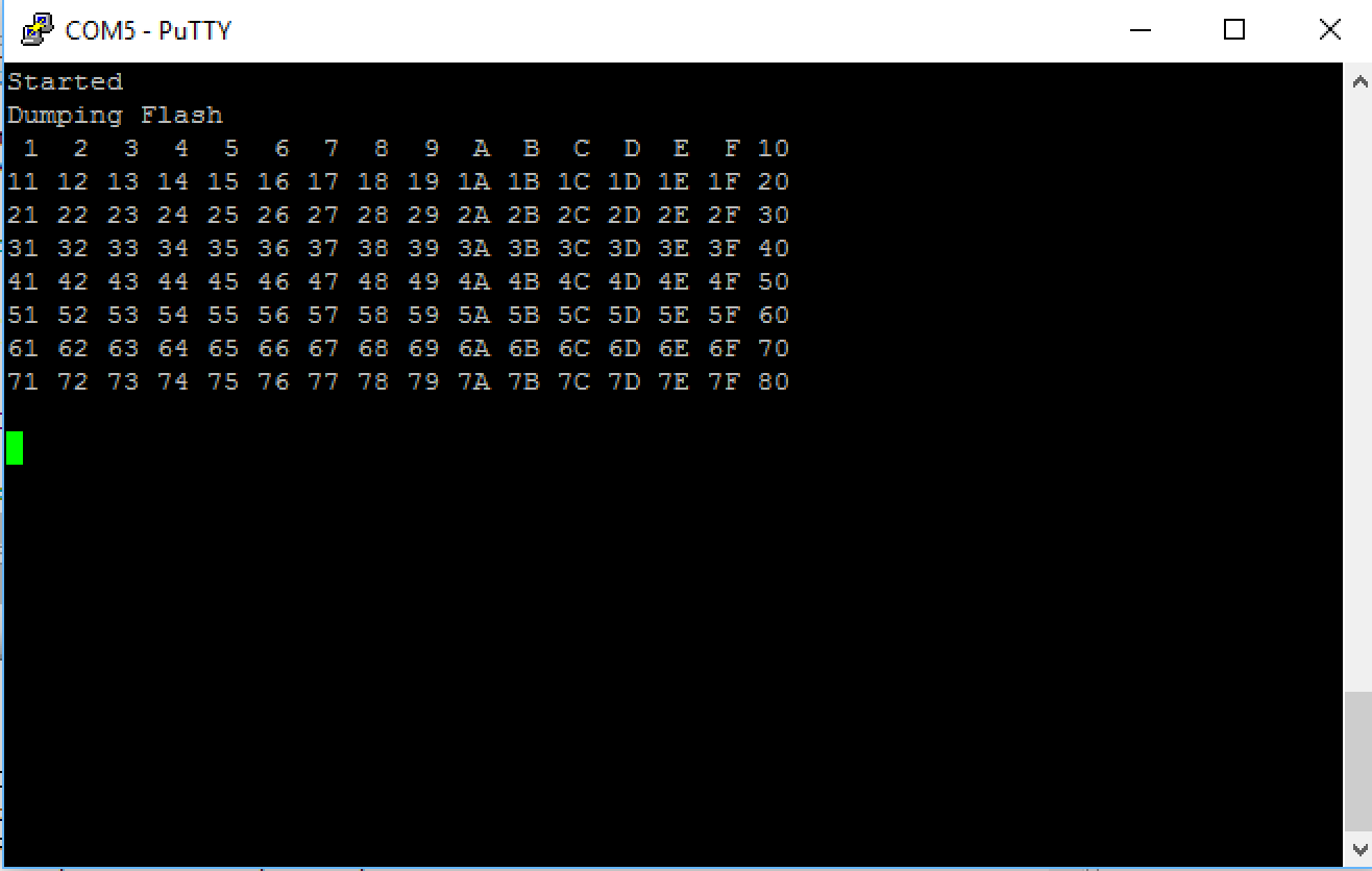
Then I hit reset on the board and press ‘f’ to printout the PSoC 4 Flash array. And I see success, the values were retained in the PSoC 4 Flash even after resetting the device. (or for that matter power cycling it)
Protecting Rows of the PSoC 4 Flash
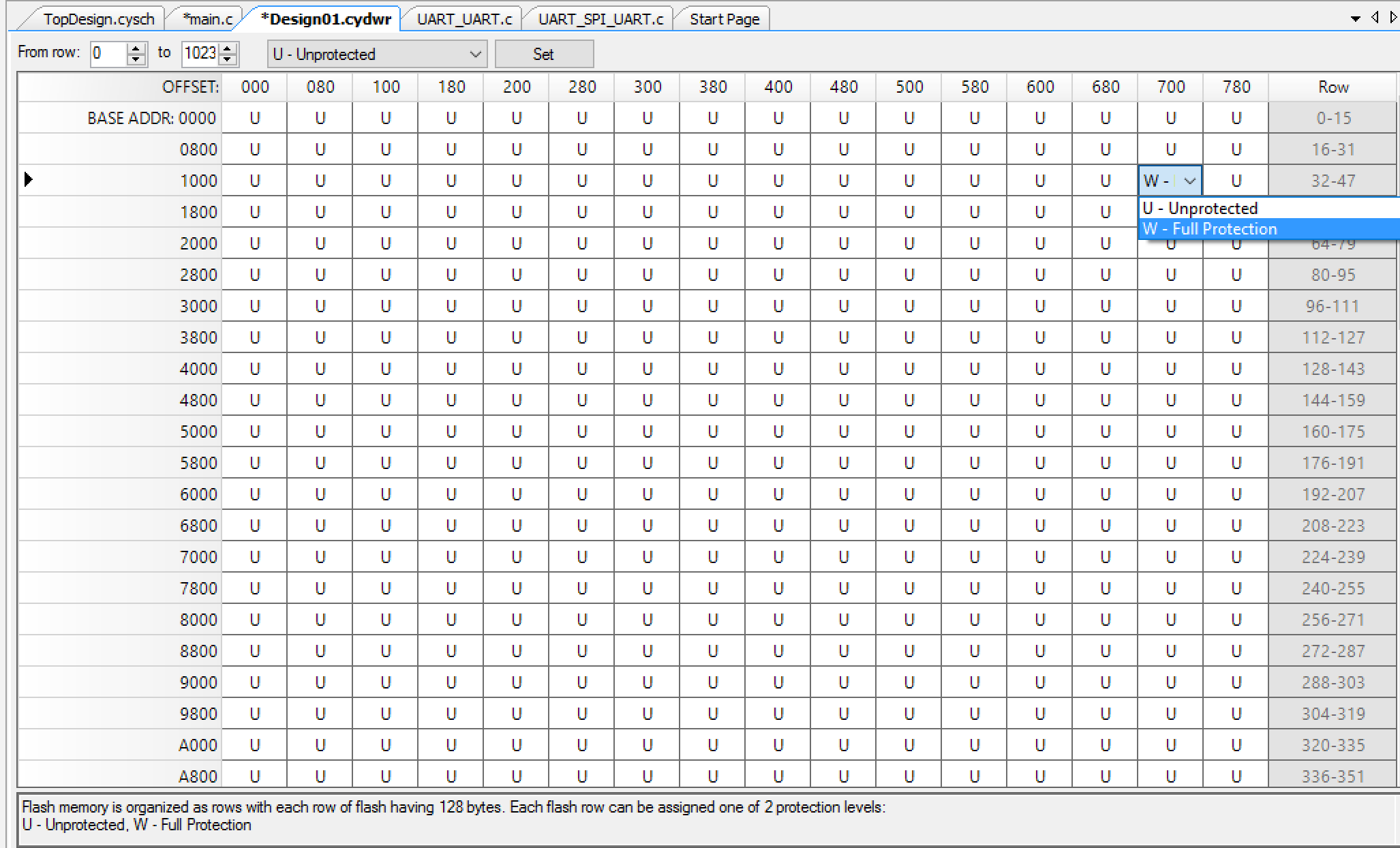
One cool feature of the PSoC 4 Flash is that you can write protect it on a row by row basis. Meaning that you can make it so that the PSoC 4 Flash writing hardware will not overwrite rows. You do this by going to the “Flash Security” tab of the Design Wide Resources. Then you have 1 box for each row in the flash where you can pick “W” for Full Protection and “U” for Writable. In the screen show below you can see me changing the row “ox1700” to Write protection. This is the row where my Flash array resides.
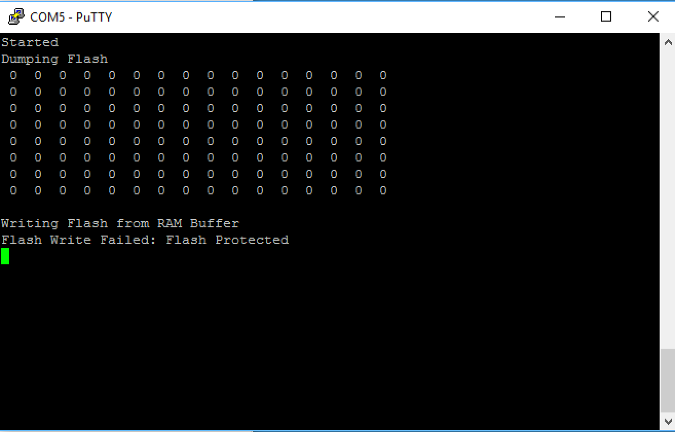
After reprogramming my device I try to press ‘w’ and you can see that the Write fails.
As always my projects are available on the IoT Expert GitHub site git@github.com:iotexpert/PSoC4-Flash-Write-Example.git


5 Comments
Hi Alan,
again, great article. Thanks!
One question: Where to find more information about the SFLASH? Some devices seems to have SFLASH, but no comment is given in the related data sheet (e.g. CY8C4247LQI-BL483) How to identify devices having SFLASH?
Regards,
Holger
In general the SFLASH is reserved for use by Cypress to setup the part. There are however somewhere between 0 and 4 rows which can be used by customers. When you build each of the part there will be a #define created by PSoC Creator that will tell you how many rows you have to use.
Alan,
How do we access the user sflash portion to save data like calibration data that wont get overwritten with a firmware update?
I have tried to use the code / api from the 100 projects for 100 days, but it fails.
I am using the CyBle-224110-00
Thanks,
Rob
You should be able to use uint32 CySysSFlashWriteUserRow(uint32 rowNum, uint8 *rowData)
There is a macro called CY_SFLASH_NUMBER_USERROWS which tells you the number of user rows.
There is another macro called CY_SFLASH_USERBASE which tells you where the 0th row of user sflash resides.
I haven’t tried it… but it should work
I tried it and it works fine… here is a little block of code
When you program this and run it the LED is red… then hit reset and the LED becomes green.
int main(void)
{
CyGlobalIntEnable; /* Enable global interrupts. */
uint8_t buff[CY_SFLASH_SIZEOF_USERROW];
uint8_t *mySFlash;
mySFlash = (uint8_t*)CY_SFLASH_USERBASE;
if(mySFlash[0] != 0x12)
{
red_Write(0);
buff[0] = 0x12;
CySysSFlashWriteUserRow(0, buff);
}
else
{
green_Write(0);
}
while(1);
}