Summary
I bought four MCU Friend 3.5″ TFT shields. And, unfortunately, they have spiraled me into a deep, dark place trying to figure out how to use them. The the documentation consists of a sticker on the antistatic bag, a picture of the shield with a list of 5 different possible LCD drivers, a pinout, and a block of code that supposedly represents the startup code. The unfortunate part is that none of these have been exactly right – they all have errors. This article is a description of the journey to figuring out how to use them.
This article has the following parts:
- MCU Friend 3.5″ Documentation
- MCU Friend 3.5″ Shields
- Using the MCUFRIEND_kbv Library
- Identify the LCD Driver with Register Reads
- A PSoC Program To Identify LCD Controllers
- Using the MCUFriend_kbv Startup Code
- Use the Web Startup
- Conclusion
MCU Friend 3.5″ Documentation
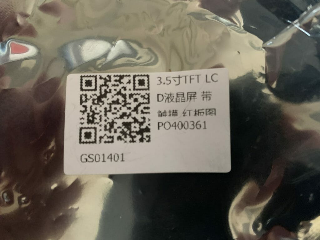
Here is a picture of the bag. (the QR code is a number “181024202132” which I thought might be a phone number but isn’t. It also doesn’t match anything in google, so i’m not sure what it is.
This text on the website says:
Features:
- 5inch TFT LCD Module, Resolution 480×320, Controller ili9481 ili9468, ili9488 hx8357, or r61581.
- Designed with a TF(Micro SD) card socket on the back of board so that you can conveniently insert a card.
- Support touch screen function.
- The test code is provided below.
- This kit requires certain professional knowledge and ability, make sure you know how to use it, please. We cannot provide any technical assistance.
Specifications:
Controller: ili9481 ili9468, ili9488 hx8357, or r61581
Resolution: 480×320
Voltage: 5V/3.3V
Package Include: 1 x LCD Module
The website also has this code which they claim is the startup code. It is interesting that
- There are several lines are commented out
- It implies that you have a SPI interface
- When you look at the commands some of them don’t exist in some of the controllers
write_SPI_commond(0xFF);
write_SPI_commond(0xFF);
delay_nms(5);
write_SPI_commond(0xFF);
write_SPI_commond(0xFF);
write_SPI_commond(0xFF);
write_SPI_commond(0xFF);
delay_nms(10);
write_SPI_commond(0xB0);
write_SPI_data(0x00);
write_SPI_commond(0xB3);
write_SPI_data(0x02);
write_SPI_data(0x00);
write_SPI_data(0x00);
write_SPI_data(0x10);
write_SPI_commond(0xB4);
write_SPI_data(0x11);//0X10
write_SPI_commond(0xC0);
write_SPI_data(0x13);
write_SPI_data(0x3B);//
write_SPI_data(0x00);
write_SPI_data(0x00);
write_SPI_data(0x00);
write_SPI_data(0x01);
write_SPI_data(0x00);//NW
write_SPI_data(0x43);
write_SPI_commond(0xC1);
write_SPI_data(0x08);
write_SPI_data(0x15);//CLOCK
write_SPI_data(0x08);
write_SPI_data(0x08);
write_SPI_commond(0xC4);
write_SPI_data(0x15);
write_SPI_data(0x03);
write_SPI_data(0x03);
write_SPI_data(0x01);
write_SPI_commond(0xC6);
write_SPI_data(0x02);
write_SPI_commond(0xC8);
write_SPI_data(0x0c);
write_SPI_data(0x05);
write_SPI_data(0x0A);//0X12
write_SPI_data(0x6B);//0x7D
write_SPI_data(0x04);
write_SPI_data(0x06);//0x08
write_SPI_data(0x15);//0x0A
write_SPI_data(0x10);
write_SPI_data(0x00);
write_SPI_data(0x31);//0x23
write_SPI_data(0x10);
write_SPI_data(0x15);//0x0A
write_SPI_data(0x06);//0x08
write_SPI_data(0x64);//0x74
write_SPI_data(0x0D);//0x0B
write_SPI_data(0x0A);//0x12
write_SPI_data(0x05);//0x08
write_SPI_data(0x0C);//0x06
write_SPI_data(0x31);//0x23
write_SPI_data(0x00);
write_SPI_commond(0x35);
write_SPI_data(0x00);
//write_SPI_commond(0x36);
//write_SPI_data(0x00);
write_SPI_commond(0x0C);
write_SPI_data(0x66);
write_SPI_commond(0x3A);
write_SPI_data(0x66);
write_SPI_commond(0x44);
write_SPI_data(0x00);
write_SPI_data(0x01);
write_SPI_commond(0xD0);
write_SPI_data(0x07);
write_SPI_data(0x07);//VCI1
write_SPI_data(0x14);//VRH 0x1D
write_SPI_data(0xA2);//BT 0x06
write_SPI_commond(0xD1);
write_SPI_data(0x03);
write_SPI_data(0x5A);//VCM  0x5A
write_SPI_data(0x10);//VDV
write_SPI_commond(0xD2);
write_SPI_data(0x03);
write_SPI_data(0x04);//0x24
write_SPI_data(0x04);
write_SPI_commond(0x11);
delay_nms(150);
write_SPI_commond(0x2A);
write_SPI_data(0x00);
write_SPI_data(0x00);
write_SPI_data(0x01);
write_SPI_data(0x3F);//320
write_SPI_commond(0x2B);
write_SPI_data(0x00);
write_SPI_data(0x00);
write_SPI_data(0x01);
write_SPI_data(0xDF);//480
//write_SPI_commond(0xB4);
//write_SPI_data(0x00);
delay_nms(100);
write_SPI_commond(0x29);
delay_nms(30);
write_SPI_commond(0x2C);
It also has a picture which says the LCD has one of several different controllers (and after digging in I know for a fact that two of mine were made by Raydium and are not on the list)
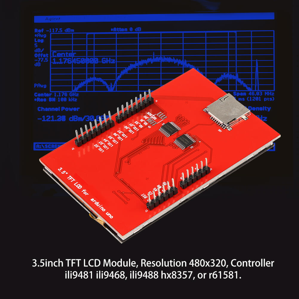
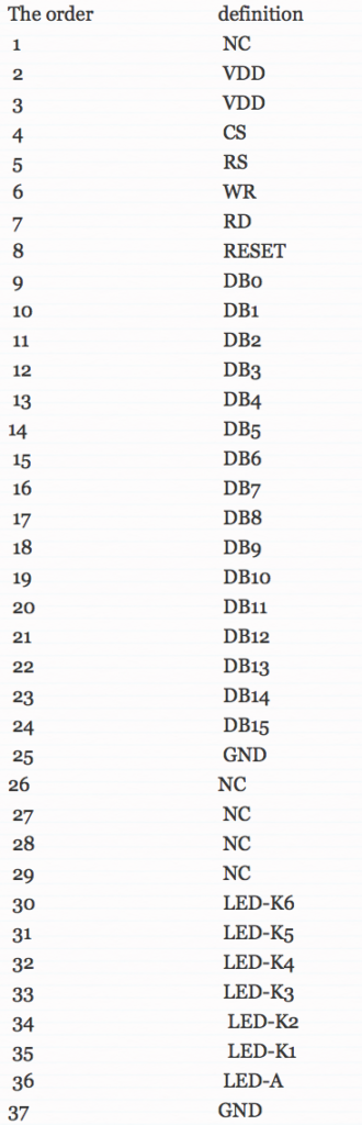
And finally a table of pins. Which is interesting as it lists 37 pins when the shield has no where near that number. And it shows the shield as 16-bit interface which it isnt … and it shows some LEDs which aren’t there either.
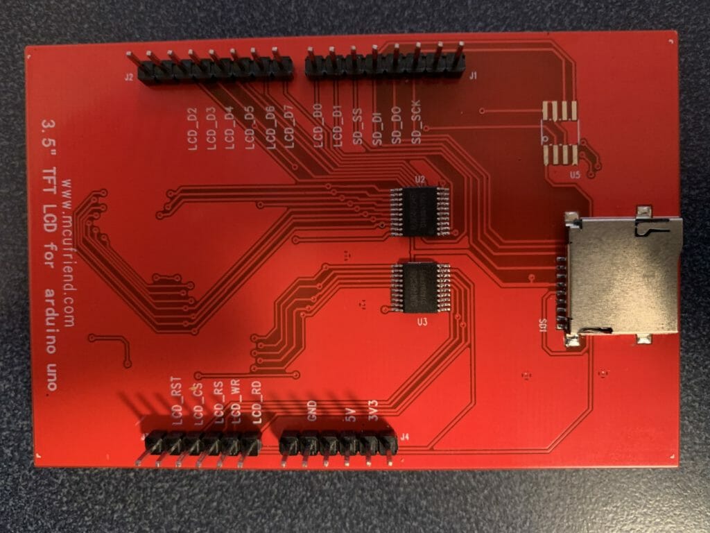
MCU Friend 3.5″ Shields
I bought 4 different shields. One came broken. The other three are all different. When you look at the boards there are two visibly different configurations
Using the MCUFRIEND_kbv Library
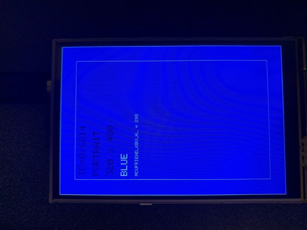
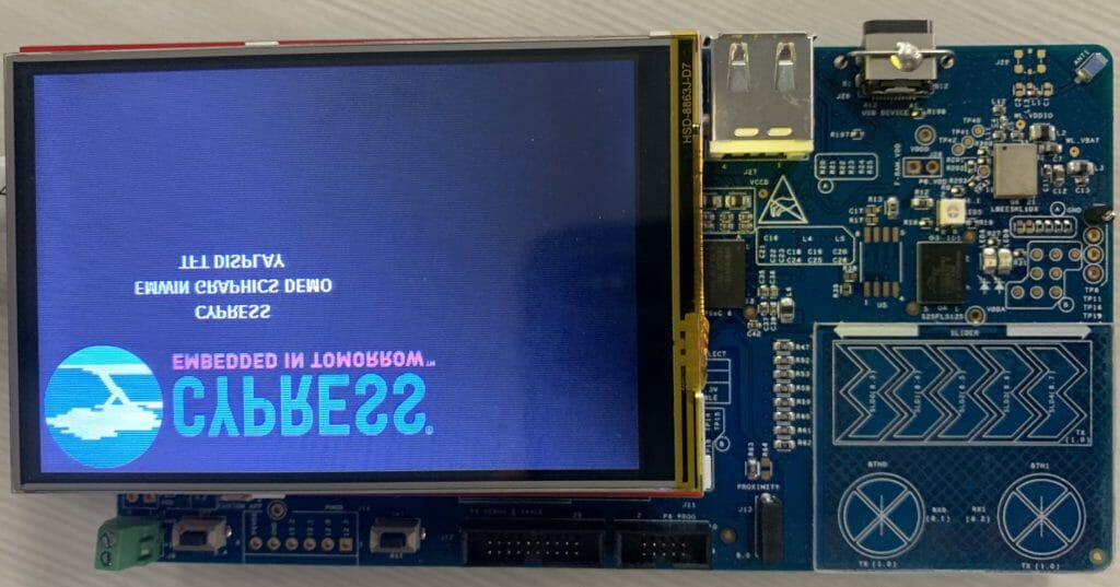
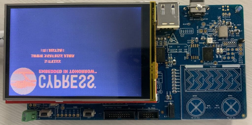
The first thing I did was try to use the MCUFRIEND_kbv library to see if the screens worked. The first board identified as ID=0x9403 and did not work. Apparently, the tool just spits out the ID if it doesn’t know it, which it did not.
One of the boards identified as ID=0x6814 worked perfectly, and one had a blue cast to all of the screens. The crazy part is the two boards that identified as ID=0x6814 had different PCBs. According to the comments in the MCUFRIEND_kbv.cpp ID=0x6814 is an RM68140 and ID=9403 is unknown.
Here is the one with the blue cast:
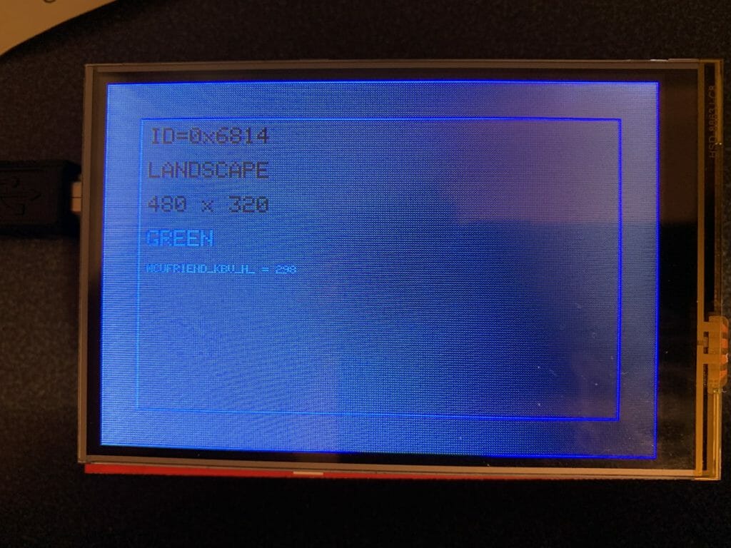
Here is the functional one:
Identify with Register Reads
Next, I started down the path of trying to figure out what the controllers were by using register reads. David Prentice (the guy who wrote/maintains the MCU Friend_kbv Arduino library) has an absolute ton of responses on the Arduino forum trying to help people figure out what their shield is. He asks them to post the register report from his example program LCD_ID_readnew which is included as an example in the library.
When you look at these LCD controllers they all have some variant of “Read ID” which responds with 1-6 bytes. The basic idea of this program is to look at what bytes are returned to try to identify the controller. Here is an example of what I got when I ran the LCD_ID_readnew program on my shields:
reg(0x0000) 00 00 ID: ILI9320, ILI9325, ILI9335, ...
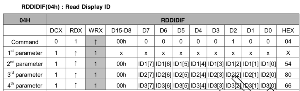
reg(0x0004) 54 54 80 66 Manufacturer ID
reg(0x0009) 00 00 61 00 00 Status Register
reg(0x000A) 08 08 Get Powsr Mode
reg(0x000C) 66 66 Get Pixel Format
reg(0x0030) 00 00 00 01 DF PTLAR
reg(0x0033) 00 00 00 01 E0 00 00 VSCRLDEF
reg(0x0061) 00 00 RDID1 HX8347-G
reg(0x0062) 00 00 RDID2 HX8347-G
reg(0x0063) 00 00 RDID3 HX8347-G
reg(0x0064) 00 00 RDID1 HX8347-A
reg(0x0065) 00 00 RDID2 HX8347-A
reg(0x0066) 00 00 RDID3 HX8347-A
reg(0x0067) 00 00 RDID Himax HX8347-A
reg(0x0070) 00 00 Panel Himax HX8347-A
reg(0x00A1) 00 00 00 00 00 RD_DDB SSD1963
reg(0x00B0) 00 00 RGB Interface Signal Control
reg(0x00B3) 00 00 11 00 00 Frame Memory
reg(0x00B4) 00 00 Frame Mode
reg(0x00B6) 02 02 02 3B 00 Display Control
reg(0x00B7) 06 06 Entry Mode Set
reg(0x00BF) FF FF 68 14 00 FF ILI9481, HX8357-B
reg(0x00C0) 0E 0E 0E 00 00 00 00 00 00 Panel Control
reg(0x00C1) 04 04 00 00 Display Timing
reg(0x00C5) 00 00 Frame Rate
reg(0x00C8) 00 00 00 00 00 00 00 00 00 00 00 00 00 GAMMA
reg(0x00CC) 00 00 Panel Control
reg(0x00D0) 00 00 00 00 Power Control
reg(0x00D1) 00 00 00 00 VCOM Control
reg(0x00D2) 00 00 00 Power Normal
reg(0x00D3) 00 00 94 86 ILI9341, ILI9488
reg(0x00D4) 00 00 00 00 Novatek
reg(0x00DA) 54 54 RDID1
reg(0x00DB) 80 80 RDID2
reg(0x00DC) 66 66 RDID3
reg(0x00E0) 00 00 54 07 44 05 08 00 54 07 44 05 08 44 44 00 GAMMA-P
reg(0x00E1) 00 00 00 00 00 00 00 00 00 00 00 00 00 00 00 00 GAMMA-N
reg(0x00EF) 00 00 00 00 00 00 ILI9327
reg(0x00F2) 00 00 00 00 00 00 00 00 00 00 00 00 Adjust Control 2
reg(0x00F6) 00 00 00 00 Interface Control
The key thing to see in this output is the register 0x04 which says 54,80,66 which identifies this as a Raydium RM68140 LCD controller. Here is a snapshot from the data sheet.
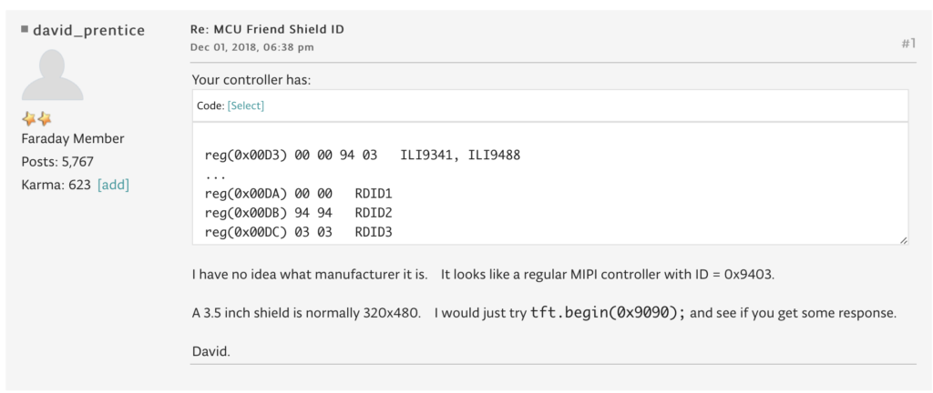
Unfortunately, the next thing to notice is that Register 0xBF has reg(0x00BF) FF FF 68 14 00 FF. The unfortunate part is that this register is not documented in the data sheet beyond this one reference:

Presumably the “68 14” corresponds to a Raydium 68140, but who knows? When I posted this on the Arduino forum, David Prentice responded (David does yeoman’s labor helping people and should be Thanked for all of his pro-bono work and putting up with a bunch of really bad questions)
After digging some more, I decided that it is super ugly out there, as you find that there are a significant number of LCD controllers that are clones, copies, pirated etc… and that they all present themselves differently. And, in hindsight I think that this is the reason that my ILI9341 from the previous article doesnt quite work correctly.
A PSoC Program To Identify LCD Controllers
The next thing that I did was create a PSoC Program to read registers from the controllers to try to figure out what they were. My original plan was to write a complete identification program, but I have largely decided that this is a waste of time (more on this later). Here is the beginning of the project, it is called “Identify” in the workspace.
First, a function to reset the screen by toggling the reset line on the controller, then sending a command “0x01” which is commonly a software reset. It turns out that I spent a bunch of time trying to figure out what was going on because I was not getting any responses from the controllers. This was caused by not sending the software reset, which at least in two of the cases makes them unresponsive.
#define LCD_COMMAND (0)
#define LCD_DATA (1)

void lcdReset()
{
       /* Reset - High, Low (reset), High */
    Cy_GPIO_Set(LCD_RESET_N_0_PORT, LCD_RESET_N_0_NUM);
    CyDelay(200);
    Cy_GPIO_Clr(LCD_RESET_N_0_PORT, LCD_RESET_N_0_NUM);
    CyDelay(200);
    Cy_GPIO_Set(LCD_RESET_N_0_PORT, LCD_RESET_N_0_NUM);
    CyDelay(200);

    GraphicLCDIntf_1_Write8(LCD_COMMAND,0x01);

}

void regReadPrint(uint8_t reg,uint8_t *buff,uint16_t num)
{
    GraphicLCDIntf_1_Write8(LCD_COMMAND,reg);
    GraphicLCDIntf_1_ReadM8(LCD_DATA,buff,num);
    printf("%02X ",reg);
    for(int i=0;i<num;i++)
    {
        printf("0x%02X,",buff[i]);
    }
    printf("\r\n");

}
Then I built a command line interface that queries the typical registers:
int main(void)
{
    uint8_t buff[128];

    __enable_irq(); /* Enable global interrupts. */

    UART_Start();
    setvbuf( stdin, NULL, _IONBF, 0 );
    printf("Started\r\n");

    GraphicLCDIntf_1_Start();
    lcdReset();

    while(1)
    {
        char c;
        c=getchar();

        switch(c)
        {
            case 'a':
                regReadPrint(0x04,buff,6);
                regReadPrint(0xA1,buff,6);
                regReadPrint(0xBF,buff,6);
                regReadPrint(0xDA,buff,1);
                regReadPrint(0xDB,buff,1);
                regReadPrint(0xDC,buff,1);
                regReadPrint(0xd3,buff,6);
            break;
When I ran this program on the three controllers here is what I got:
Screen 1:
04 0x00,0x00,0x94,0x03,0x00,0x00,
A1 0x00,0x00,0x00,0x00,0x00,0x00,
BF 0x00,0x00,0x00,0x00,0x00,0x00,
DA 0x00,
DB 0x94,
DC 0x03,
D3 0x00,0x00,0x94,0x03,0x00,0x00,

Screen 2: Raydium 68140 (arduino works)
04 0x54,0x54,0x80,0x66,0x00,0x00,
BF 0xFF,0xFF,0x68,0x14,0x00,0xFF,
DA 0x54,
DB 0x80,
DC 0x66,
D3 0x00,0x00,0x94,0x86,0x00,0x00,

Screen 3: Raydium 68140 (looks blue)
04 0x54,0x54,0x80,0x66,0x00,0x00,
BF 0xFF,0xF7,0x60,0x14,0x00,0xFF,
DA 0x54,
DB 0x80,
DC 0x66,
D3 0x00,0x00,0x94,0x86,0x00,0x00,
So, where does this leave me?
- I have no idea what Screen 1 is? 04 0x00,0x00,0x94,0x03,0x00,0x00,
- Two of them appear to be Raydium RM68140s
- The two Raydiums have different register values for 0xBF
And all of this is insane because most of these companies don’t appear to have coherent websites or generally available datasheets. I suppose that it would help if I spoke and read Chinese.
Using the MCUFriend_kbv Startup Code
The next thing that I did was try out the startup code that MCUFriend_kbv generates. I used the same technique from PSoC 6 + Segger EmWin + MCUFriend 2.4″ Part 1 and spit out the startup bytes. Here they are:
0x1,0x0,
0x28,0x0,
0x3A,0x1,0x55,
0x3A,0x1,0x55,
0x11,0x0,
0x29,0x0,
0xB6,0x3,0x0,0x22,0x3B,
0x36,0x1,0x8,
0x2A,0x4,0x0,0x0,0x1,0x3F,
0x2B,0x4,0x0,0x0,0x1,0xDF,
0x33,0x6,0x0,0x0,0x1,0xE0,0x0,0x0,
0x37,0x2,0x0,0x0,
0x13,0x0,
0x20,0x0,
And this is what it looks like in my PSoC program:
static const uint8_t mcu35_init_sequence_kbv[]  = {
    0x1,0x0,                            // Software Reset
    0x28,0x0,                           // Display Off
    0x3A,0x1,0x55,                      // Pixel Format Set 565
    0x3A,0x1,0x55,                      // Pixel Format Set 565
    0x11,0x0,                           // Sleep Out
    0x29,0x0,                           // Display On
    0xB6,0x3,0x0,0x22,0x3B,             // Display Function Control
    0x36,0x1,0x8,                       // Memory Access Control
    0x2A,0x4,0x0,0x0,0x1,0x3F,          // Column Set Address 320
    0x2B,0x4,0x0,0x0,0x1,0xDF,          // Page Set Addres 480
    0x33,0x6,0x0,0x0,0x1,0xE0,0x0,0x0,  // Vertical Scrolling Definition
    0x37,0x2,0x0,0x0,                   // Vertical Scrolling Start Address
    0x13,0x0,                           // Normal Display On
    0x20,0x0,                           // Display Inversion Off
};
When I run this things look like this:
Screen 1: Looks good, just need to flip the x-axis
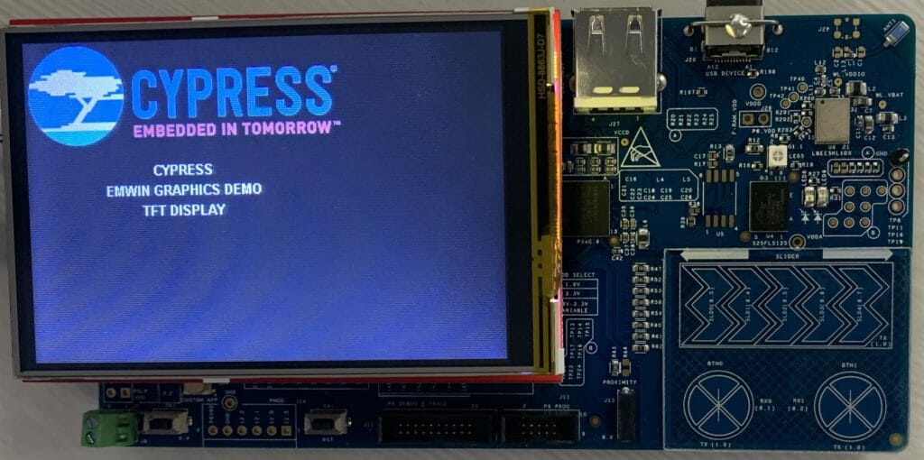
Screen 2: Looks good, just need to flip the y-axis
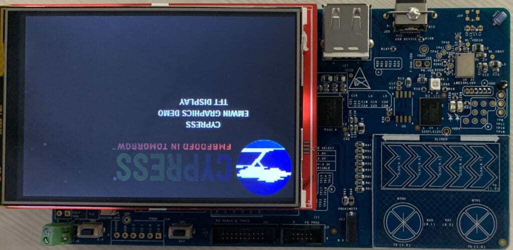
Screen 3: Not good… not exactly sure how to fix.
Use the Web Startup
Well, things still aren’t quite right, so for some strange reason, I keep going and try to use the startup code from the web. In order to make it work I translate
- delay_nms –> CyDelay
- write_SPI_commond –> GraphicLCDIntf_1_Write8_A0
- write_SPI_data –> GraphicLCDIntf_1_Write8_A1
Here is the updated code:
static void _InitController35Web()
{
    GraphicLCDIntf_1_Write8_A0(0xFF);
    GraphicLCDIntf_1_Write8_A0(0xFF);
    CyDelay(5);
    GraphicLCDIntf_1_Write8_A0(0xFF);
    GraphicLCDIntf_1_Write8_A0(0xFF);
    GraphicLCDIntf_1_Write8_A0(0xFF);
    GraphicLCDIntf_1_Write8_A0(0xFF);
    CyDelay(10);
    //0xB0,0x01,0x00,
    GraphicLCDIntf_1_Write8_A0(0xB0); //0
    GraphicLCDIntf_1_Write8_A1(0x00);

    //0xB3,0x04,0x02,0x00,0x00,0x10,
    GraphicLCDIntf_1_Write8_A0(0xB3); //1
    GraphicLCDIntf_1_Write8_A1(0x02);
    GraphicLCDIntf_1_Write8_A1(0x00);
    GraphicLCDIntf_1_Write8_A1(0x00);
    GraphicLCDIntf_1_Write8_A1(0x10);

    //0xB4,0x01,0x11,
    GraphicLCDIntf_1_Write8_A0(0xB4); // 2
    GraphicLCDIntf_1_Write8_A1(0x11);//0X10

    // 0xC0,0x08,0x13,0x3B,0x00,0x00,0x00,0x01,0x00,0x43,
    GraphicLCDIntf_1_Write8_A0(0xC0);
    GraphicLCDIntf_1_Write8_A1(0x13);
    GraphicLCDIntf_1_Write8_A1(0x3B);//
    GraphicLCDIntf_1_Write8_A1(0x00);
    GraphicLCDIntf_1_Write8_A1(0x00);
    GraphicLCDIntf_1_Write8_A1(0x00);
    GraphicLCDIntf_1_Write8_A1(0x01);
    GraphicLCDIntf_1_Write8_A1(0x00);//NW
    GraphicLCDIntf_1_Write8_A1(0x43);

    // 0xC1,0x04,0x08,0x15,0x08,0x08,
    GraphicLCDIntf_1_Write8_A0(0xC1);
    GraphicLCDIntf_1_Write8_A1(0x08);
    GraphicLCDIntf_1_Write8_A1(0x15);//CLOCK
    GraphicLCDIntf_1_Write8_A1(0x08);
    GraphicLCDIntf_1_Write8_A1(0x08);

    // 0xC4,0x04,0x15,0x03,0x03,0x01
    GraphicLCDIntf_1_Write8_A0(0xC4);
    GraphicLCDIntf_1_Write8_A1(0x15);
    GraphicLCDIntf_1_Write8_A1(0x03);
    GraphicLCDIntf_1_Write8_A1(0x03);
    GraphicLCDIntf_1_Write8_A1(0x01);

    // 0xC6,0x01,0x02
    GraphicLCDIntf_1_Write8_A0(0xC6);
    GraphicLCDIntf_1_Write8_A1(0x02);

    // 0xC8,0x15,0x0C,0x05,0x0A,0x6B,0x04,0x06,0x15,0x10,0x00,0x31,0x10,0x15,0x06,0x64,0x0D,0x0A,0x05,0x0C,0x31,0x00
    GraphicLCDIntf_1_Write8_A0(0xC8);
    GraphicLCDIntf_1_Write8_A1(0x0c);
    GraphicLCDIntf_1_Write8_A1(0x05);
    GraphicLCDIntf_1_Write8_A1(0x0A);//0X12
    GraphicLCDIntf_1_Write8_A1(0x6B);//0x7D
    GraphicLCDIntf_1_Write8_A1(0x04);
    GraphicLCDIntf_1_Write8_A1(0x06);//0x08
    GraphicLCDIntf_1_Write8_A1(0x15);//0x0A
    GraphicLCDIntf_1_Write8_A1(0x10);
    GraphicLCDIntf_1_Write8_A1(0x00);
    GraphicLCDIntf_1_Write8_A1(0x31);//0x23
    GraphicLCDIntf_1_Write8_A1(0x10);
    GraphicLCDIntf_1_Write8_A1(0x15);//0x0A
    GraphicLCDIntf_1_Write8_A1(0x06);//0x08
    GraphicLCDIntf_1_Write8_A1(0x64);//0x74
    GraphicLCDIntf_1_Write8_A1(0x0D);//0x0B
    GraphicLCDIntf_1_Write8_A1(0x0A);//0x12
    GraphicLCDIntf_1_Write8_A1(0x05);//0x08
    GraphicLCDIntf_1_Write8_A1(0x0C);//0x06
    GraphicLCDIntf_1_Write8_A1(0x31);//0x23
    GraphicLCDIntf_1_Write8_A1(0x00);

    // 0x35,0x01,0x00
    GraphicLCDIntf_1_Write8_A0(0x35);
    GraphicLCDIntf_1_Write8_A1(0x00);
    //GraphicLCDIntf_1_Write8_A0(0x36);
    //GraphicLCDIntf_1_Write8_A1(0x00);

    // 0x0C,0x01,x066
    GraphicLCDIntf_1_Write8_A0(0x0C);
    GraphicLCDIntf_1_Write8_A1(0x66);

    //0x3A,0x01,0x55
    GraphicLCDIntf_1_Write8_A0(0x3A);
    GraphicLCDIntf_1_Write8_A1(0x55); // ARH changed to 565
    //GraphicLCDIntf_1_Write8_A1(0x66);

    // 0x44,0x02,0x00,0x01
    GraphicLCDIntf_1_Write8_A0(0x44);
    GraphicLCDIntf_1_Write8_A1(0x00);
    GraphicLCDIntf_1_Write8_A1(0x01);

    // 0xD0,0x04,0x07,0x07,0x14,0xA2,
    GraphicLCDIntf_1_Write8_A0(0xD0);
    GraphicLCDIntf_1_Write8_A1(0x07);
    GraphicLCDIntf_1_Write8_A1(0x07);//VCI1
    GraphicLCDIntf_1_Write8_A1(0x14);//VRH 0x1D
    GraphicLCDIntf_1_Write8_A1(0xA2);//BT 0x06


    // 0xD1,0x03,0x03,0x5A,0x10
    GraphicLCDIntf_1_Write8_A0(0xD1);
    GraphicLCDIntf_1_Write8_A1(0x03);
    GraphicLCDIntf_1_Write8_A1(0x5A);//VCM  0x5A
    GraphicLCDIntf_1_Write8_A1(0x10);//VDV

    // 0xD2,0x03,0x03,0x04,0x04,
    GraphicLCDIntf_1_Write8_A0(0xD2);
    GraphicLCDIntf_1_Write8_A1(0x03);
    GraphicLCDIntf_1_Write8_A1(0x04);//0x24
    GraphicLCDIntf_1_Write8_A1(0x04);

    // 0x11,0x00,
    GraphicLCDIntf_1_Write8_A0(0x11);
    CyDelay(150);


    // 0x2A,0x04,0x00,0x00,0x01,0x3F
    GraphicLCDIntf_1_Write8_A0(0x2A);
    GraphicLCDIntf_1_Write8_A1(0x00);
    GraphicLCDIntf_1_Write8_A1(0x00);
    GraphicLCDIntf_1_Write8_A1(0x01);
    GraphicLCDIntf_1_Write8_A1(0x3F);//320


    // 0x2B,0x04,0x00,0x00,0x01,0xDF
    GraphicLCDIntf_1_Write8_A0(0x2B);
    GraphicLCDIntf_1_Write8_A1(0x00);
    GraphicLCDIntf_1_Write8_A1(0x00);
    GraphicLCDIntf_1_Write8_A1(0x01);
    GraphicLCDIntf_1_Write8_A1(0xDF);//480
    //GraphicLCDIntf_1_Write8_A0(0xB4);
    //GraphicLCDIntf_1_Write8_A1(0x00);

    CyDelay(100);

    // 0x29,0x00
    GraphicLCDIntf_1_Write8_A0(0x29);
    CyDelay(30);


    // 0x2C,0x00
    GraphicLCDIntf_1_Write8_A0(0x2C);
}
Here is what I get:
Screen1: Looks good, but inverted (I know how to fix)
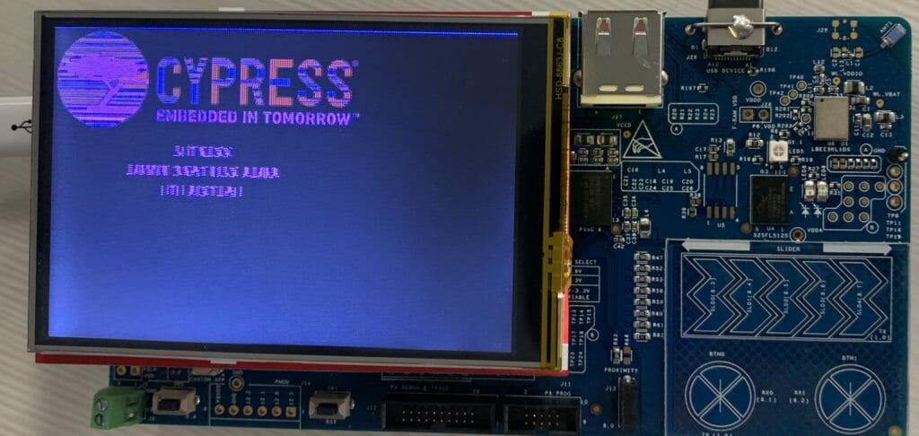
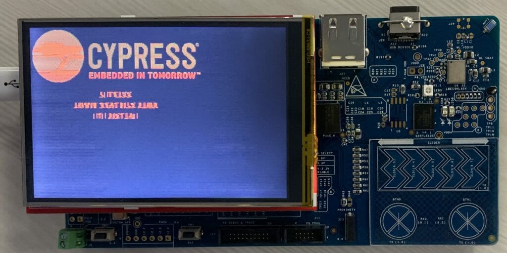
Screen 2: Looks right, except for the blue-line at the top (who knows)
Screen 3: Seriously jacked
Earlier I told you that I much preferred to use the more compact startup code. In order to match this, I decided to add a new code “0xDD” which means delay. (I hope that there are no controllers out there that use 0XDD). Here is the updated function:
static void sendStartSequence(const uint8_t *buff,uint32_t len)
{
    for(unsigned int i=0;i<len;i++)
    {
        if(buff[i] == 0xDD) //
        {
            CyDelay(buff[i+1]);
            i=i+1;
        }
        else
        {
            GraphicLCDIntf_1_Write8_A0(buff[i]);
            i=i+1;
            unsigned int count;
            count = buff[i];
            for(unsigned int j=0;j<count;j++)
            {
                i=i+1;
                GraphicLCDIntf_1_Write8_A1(buff[i]);
            }
        }
    }
}
And when I translate the web based startup code, here is what it looks like:
static const uint8_t mcu35_init_sequence_web[]  = {
    0xFF,0x00,          // ?
    0xFF,0x00,          // ?
    0xDD,5,             // Delay 5
    0xFF,0x00,          //
    0xFF,0x00,          //
    0xFF,0x00,          //
    0xFF,0x00,          // ?
    0xDD,10,            // delay 10
    //
    0xB0,0x01,0x00,                                     // IF Mode control
    0xB3,0x04,0x02,0x00,0x00,0x10,                      // Frame Rate Control - only 2 paramters
    0xB4,0x01,0x11,                                     // Display inversion control
    0xC0,0x08,0x13,0x3B,0x00,0x00,0x00,0x01,0x00,0x43,  // Power Control 1
    0xC1,0x04,0x08,0x15,0x08,0x08,                      // Power Control 2
    0xC4,0x04,0x15,0x03,0x03,0x01,                      // ?
    0xC6,0x01,0x02,                                     // ?
    // ??
    0xC8,0x15,0x0C,0x05,0x0A,0x6B,0x04,0x06,0x15,0x10,0x00,0x31,0x10,0x15,0x06,0x64,0x0D,0x0A,0x05,0x0C,0x31,0x00,
    0x35,0x01,0x00,                     // Tearing Effect
    0x0C,0x01,0x66,                     // Read pixel format?
    0x3A,0x01,0x55,                     // Pixel Format Set

    0x44,0x02,0x00,0x01,                // Set Tear Scanline
    0xD0,0x04,0x07,0x07,0x14,0xA2,      // NVM Write
    0xD1,0x03,0x03,0x5A,0x10,           // NVM Protection Key
    0xD2,0x03,0x03,0x04,0x04,           // NVM Status Read

    0x11,0x00,                          // Sleep Out
    0xDD,150,                           // Delay 150ms
    0x2A,0x04,0x00,0x00,0x01,0x3F,      // Column Set Address 320
    0x2B,0x04,0x00,0x00,0x01,0xDF,      // Page Set Address   480
    0xDD,100,                           // Delay 100ms
    0x29,0x00,                          // Display On
    0xDD,30,                            // delay 30ms
    0x2C,0x00                           // Memory Write
};
Notice that my comments on the commands show that there are a bunch of them I dont know what they mean. Moreover, the MIPI spec says that all of the commands after 0xAF are reserved for the manufacturer… so I am pretty sure that they don’t do anything, or maybe should’nt be used?. The last thing that I decide to do is edit out the stuff that does not seem to make sense. Here is the new sequence:
static const uint8_t mcu35_init_sequence_web_edited[]  = {
    0x35,0x01,0x00,                     // Tearing Effect
    0x3A,0x01,0x55,                     // Pixel Format Set
    0x44,0x02,0x00,0x01,                // Set Tear Scanline
    0x11,0x00,                          // Sleep Out
    0xDD,150,                           // Delay 150ms
    0x2A,0x04,0x00,0x00,0x01,0x3F,      // Column Set Address 320
    0x2B,0x04,0x00,0x00,0x01,0xDF,      // Page Set Address   480
    0xDD,100,                           // Delay 100ms
    0x29,0x00,                          // Display On
    0xDD,30,                            // delay 30ms
};
When I run this code I get the following screens:
Screen 1: Looks good, but inverted
Screen 2: Looks good (one of those codes created the blue line that is now gone)
Screen 3: Color screwed up
Conclusion
At this point I have spent a frightening amount of time figuring out how these screens work. Although it has been a good learning experience, I have generally decided that using unknown displays from China with LCD drivers of questionable origin is not worth the pain of trying to sort out the interface. Beyond that:
- emWin seems to be able to talk to the RM68140 even though it is not listed as a supported chip
- I have no idea what to do about screen 3. Is it physically broken? Or do I just not know how to talk to it?
- There many counterfeit chips out there.. and although they may work, it probably isnt worth the effort
- David Prentice has added a lot of value for no personal gain by supporting the Arduino library MCUFriend_kbv
Embedded Graphics Index