
Summary – Initializing the PSoC
Well, I have finally reached the end of the booting the PSoC4 series. Actually I am contemplating one more article after this one, but for now I am done. In this article I talk about the function “initialize_psoc()” which is responsible for initializing the PSoC; it turns the PSoC into a PSoC. The function does two basic things:
- It moves the exception table out of the flash (at location 0x0000) and puts it into the SRAM
- It calls cyfitter_cfg() which calls a bunch of functions to setup all of the configuration registers inside of the PSoC
Here is the actual function:
/*******************************************************************************
* Function Name: initialize_psoc
******************************************************************************
*
* This function is used to initialize the PSoC chip before calling main.
*
*******************************************************************************/
#if(defined(__GNUC__) && !defined(__ARMCC_VERSION))
__attribute__ ((constructor(101)))
#endif  /* (defined(__GNUC__) && !defined(__ARMCC_VERSION)) */
void initialize_psoc(void)
{
    uint32 indexInit;

    #if(CY_IP_CPUSSV2)
        #if (CY_IP_CPUSS_CM0)
            /***********************************************************************
            * Make sure that Vector Table is located at 0000_0000 in Flash, before
            * accessing RomVectors or calling functions that may be placed in
            * .psocinit (cyfitter_cfg and ClockSetup). Note The CY_CPUSS_CONFIG_REG
            * register is retention for the specified device family.
            ***********************************************************************/
            CY_CPUSS_CONFIG_REG &= (uint32) ~CY_CPUSS_CONFIG_VECT_IN_RAM;
        #endif /* (CY_IP_CPUSS_CM0) */
    #endif  /* (CY_IP_CPUSSV2) */

    /* Set Ram interrupt vectors to default functions. */
    for (indexInit = 0u; indexInit < CY_NUM_VECTORS; indexInit++)
    {
        CyRamVectors[indexInit] = (indexInit < CY_NUM_ROM_VECTORS) ?
            #if defined (__ICCARM__)
                __vector_table[indexInit].__fun : &IntDefaultHandler;
            #else
                RomVectors[indexInit] : &IntDefaultHandler;
            #endif  /* defined (__ICCARM__) */
    }

    /* Initialize configuration registers. */
    cyfitter_cfg();

    #if !defined (__ICCARM__)
        /* Actually, no need to clean this variable, just to make compiler happy. */
        cySysNoInitDataValid = 0u;
    #endif  /* !defined (__ICCARM__) */

    #if (CYDEV_PROJ_TYPE != CYDEV_PROJ_TYPE_STANDARD)

        /* Need to make sure that this variable will not be optimized out */
        if (0u == cyBtldrRunType)
        {
            cyBtldrRunType = 0u;
        }

    #endif  /* (CYDEV_PROJ_TYPE != CYDEV_PROJ_TYPE_STANDARD) */

    #if (CY_IP_CPUSS_CM0)
        /* Vector Table is located at 0x2000:0000 in SRAM */
        CY_CPUSS_CONFIG_REG |= CY_CPUSS_CONFIG_VECT_IN_RAM;
	#else
	(*(uint32 *)CYREG_CM0P_VTOR) = CY_CPUSS_CONFIG_VECT_ADDR_IN_RAM;
    #endif /* (CY_IP_CPUSS_CM0) */
}
Move the Exception Table
In a previous article I talked about setting up the exception table and programming it into the flash. This leaves me with a previously unstated question: How do I change the address of an interrupt vector service routine? Does it have to remain static and known a priori when you write the firmware? In the Cortex-M0 architecture the answer to that question is fascinating (in my opinion). If you use the ARM CM0 “straight out of the box” the answer is you can’t. However, in the PSoC implementation of the CM0’s our system architect created a register to allow you to move the vector table.
Before I explain how this happens I would like to give a nod to the Cypress “CPUSS Architect”. He is a former NXP engineer from the Netherlands and is one of the most amazing individual talents I have ever known. He understands how to balance the white-tower-purity of the CTO office and the overall system architecture with the roll-up-your-sleeves realities of making chips.
Anyway. Maybe it is a common thing to do with the CM0 (I actually haven’t looked at other people’s implementations) but the register “CPUSS_CONFIG” changes the address logic in the CM0 to read from two different places when the vector table addresses are issues by the CPU. What this means is when the bit “CPUSS_VECS_IN_RAM” is 0, the addresses 0x0 are read from the flash, and when the bit is set to 1, the address 0x0 are read from 0x20000000 (which is the RAM).
Here is a clip from the PSoC Technical Reference Manual:
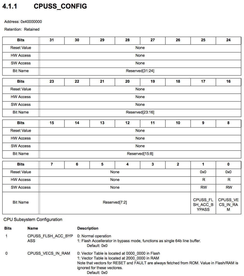
Once you see this, it is easy to understand lines 496–>517. They basically:
- Set the CPUSS_VECS_IN_RAM bit to 0
- Then copy the vector table from the flash to the RAM
Finally on lines 537–>542 it sets the bit to 1 so that the vectors are read from the flash.
The only other trick here is that the CM0+ (and CM3/CM4) have a register called “VTOR” which allows you the accomplish exactly the same thing with out having to modify the address logic in the core.
Initializing the PSoC: Call cyfitter_cfg()
As part of building a PSoC project, PSoC Creator runs a “fitter”. The fitter is responsible for
- Configuring the Digital Signal Interconnect (DSI) matrix
- Configuring the UDBs
- Configuring the Analog Routing
- Configuring the Clocks
- Assigning the blocks of the PSoC to pins and components
All of the fitter tasks get turned into C-code which are either #defines (in the case of the components) or actual c-functions and data (as in the case of 1-4). The last step in the function “start_c()” is calling the “cyfitter_cfg()” function”. The “cyfitter_cfg()” will grow and shrink depending on how you configure the UDBs and the DSI. For example, the version below has a blank schematic. In it you can see that:
- Lines 247-251 write 0s to the configuration registers… basically turning everything off
- Lines 254-265 enable the UDBs and routing
- Line 274 turns on the clocks
- Line 277 turns on the analog
/*******************************************************************************
* Function Name: cyfitter_cfg
********************************************************************************
* Summary:
*  This function is called by the start-up code for the selected device. It
*  performs all of the necessary device configuration based on the design
*  settings.  This includes settings from the Design Wide Resources (DWR) such
*  as Clocks and Pins as well as any component configuration that is necessary.
*
* Parameters:
*   void
*
* Return:
*   void
*
*******************************************************************************/
CY_CFG_SECTION
void cyfitter_cfg(void)
{
	/* Disable interrupts by default. Let user enable if/when they want. */
	CyGlobalIntDisable;

	{

		CYPACKED typedef struct {
			void CYFAR *address;
			uint16 size;
		} CYPACKED_ATTR cfg_memset_t;

		static const cfg_memset_t CYCODE cfg_memset_list [] = {
			/* address, size */
			{(void CYFAR *)(CYDEV_UDB_P0_U0_BASE), 1024u},
			{(void CYFAR *)(CYDEV_UDB_DSI0_BASE), 1024u},
		};

		uint8 CYDATA i;

		/* Zero out critical memory blocks before beginning configuration */
		for (i = 0u; i < (sizeof(cfg_memset_list)/sizeof(cfg_memset_list[0])); i++)
		{
			const cfg_memset_t CYCODE * CYDATA ms = &cfg_memset_list[i];
			CYMEMZERO(ms->address, (size_t)(uint32)(ms->size));
		}

		/* HSIOM Starting address: CYDEV_HSIOM_BASE */
		CY_SET_XTND_REG32((void CYFAR *)(CYREG_HSIOM_PORT_SEL3), 0x0000EE00u);

		/* UDB_PA_3 Starting address: CYDEV_UDB_PA3_BASE */
		CY_SET_XTND_REG32((void CYFAR *)(CYDEV_UDB_PA3_BASE), 0x00990000u);

		/* Enable digital routing */
		CY_SET_XTND_REG8((void *)CYREG_UDB_UDBIF_BANK_CTL, CY_GET_XTND_REG8((void *)CYREG_UDB_UDBIF_BANK_CTL) | 0x02u);

		/* Enable UDB array */
		CY_SET_XTND_REG8((void *)CYREG_UDB_UDBIF_WAIT_CFG, (uint8)((CY_GET_XTND_REG8((void *)CYREG_UDB_UDBIF_WAIT_CFG) & 0xC3u) | 0x14u));
		CY_SET_XTND_REG8((void *)CYREG_UDB_UDBIF_BANK_CTL, (uint8)(CY_GET_XTND_REG8((void *)CYREG_UDB_UDBIF_BANK_CTL) | 0x16u));
	}

	/* Perform second pass device configuration. These items must be configured in specific order after the regular configuration is done. */
	/* IOPINS0_3 Starting address: CYDEV_GPIO_PRT3_BASE */
	CY_SET_XTND_REG32((void CYFAR *)(CYREG_GPIO_PRT3_PC), 0x00000D80u);


	/* Setup clocks based on selections from Clock DWR */
	ClockSetup();

	/* Perform basic analog initialization to defaults */
	AnalogSetDefault();

}
However, if you had a more complicated schematic, like this one which uses a UDB and the DSI to implement a LUT
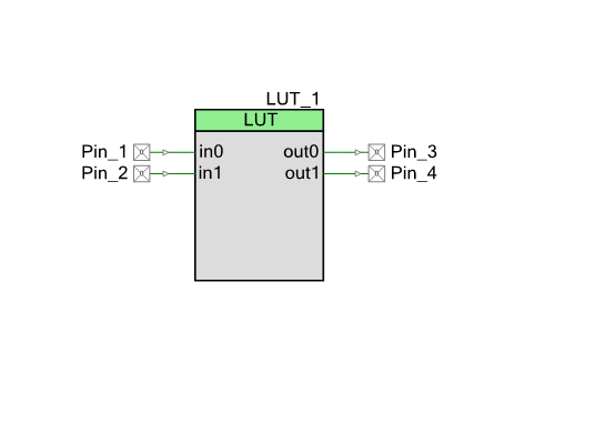
Then you will end up with a block of code that configures the DSI and UDB registers required to implement the LUT and route it to the pins. You can see on lines 274-308 there is a table of register values which are copied into the architectural registers by the function call on line 333. I started looking through the meaning of all of these register values in the TRM but realized that it didn’t matter. PSoC Creator does a perfectly good job of setting up the UDB and getting it routed to the right place.
/*******************************************************************************
* Function Name: cyfitter_cfg
********************************************************************************
* Summary:
*  This function is called by the start-up code for the selected device. It
*  performs all of the necessary device configuration based on the design
*  settings.  This includes settings from the Design Wide Resources (DWR) such
*  as Clocks and Pins as well as any component configuration that is necessary.
*
* Parameters:
*   void
*
* Return:
*   void
*
*******************************************************************************/
CY_CFG_SECTION
void cyfitter_cfg(void)
{
	/* Disable interrupts by default. Let user enable if/when they want. */
	CyGlobalIntDisable;

	{
		static const uint32 CYCODE cy_cfg_addr_table[] = {
			0x400F3007u, /* Base address: 0x400F3000 Count: 7 */
			0x400F3107u, /* Base address: 0x400F3100 Count: 7 */
			0x400F3301u, /* Base address: 0x400F3300 Count: 1 */
			0x400F4009u, /* Base address: 0x400F4000 Count: 9 */
			0x400F4102u, /* Base address: 0x400F4100 Count: 2 */
		};

		static const cy_cfg_addrvalue_t CYCODE cy_cfg_data_table[] = {
			{0x88u, 0x01u},
			{0xA0u, 0x01u},
			{0xB6u, 0x01u},
			{0xB8u, 0x80u},
			{0xBEu, 0x40u},
			{0xD8u, 0x04u},
			{0xDFu, 0x01u},
			{0x04u, 0x10u},
			{0x15u, 0x01u},
			{0x1Fu, 0x80u},
			{0x80u, 0x10u},
			{0x85u, 0x01u},
			{0xC0u, 0x40u},
			{0xC4u, 0x10u},
			{0xAFu, 0x80u},
			{0x00u, 0x20u},
			{0x04u, 0x08u},
			{0x57u, 0x20u},
			{0x80u, 0x04u},
			{0x84u, 0x10u},
			{0xC0u, 0x60u},
			{0xD4u, 0x40u},
			{0xE0u, 0x10u},
			{0xE4u, 0x80u},
			{0xAFu, 0x20u},
			{0xEEu, 0x10u},
		};


		CYPACKED typedef struct {
			void CYFAR *address;
			uint16 size;
		} CYPACKED_ATTR cfg_memset_t;

		static const cfg_memset_t CYCODE cfg_memset_list [] = {
			/* address, size */
			{(void CYFAR *)(CYDEV_UDB_P0_U0_BASE), 1024u},
			{(void CYFAR *)(CYDEV_UDB_DSI0_BASE), 1024u},
		};

		uint8 CYDATA i;

		/* Zero out critical memory blocks before beginning configuration */
		for (i = 0u; i < (sizeof(cfg_memset_list)/sizeof(cfg_memset_list[0])); i++)
		{
			const cfg_memset_t CYCODE * CYDATA ms = &cfg_memset_list[i];
			CYMEMZERO(ms->address, (size_t)(uint32)(ms->size));
		}

		cfg_write_bytes32(cy_cfg_addr_table, cy_cfg_data_table);

		/* HSIOM Starting address: CYDEV_HSIOM_BASE */
		CY_SET_XTND_REG32((void CYFAR *)(CYDEV_HSIOM_BASE), 0x00003003u);
		CY_SET_XTND_REG32((void CYFAR *)(CYREG_HSIOM_PORT_SEL3), 0x0000EE00u);

		/* UDB_PA_0 Starting address: CYDEV_UDB_PA0_BASE */
		CY_SET_XTND_REG32((void CYFAR *)(CYDEV_UDB_PA0_BASE), 0x00990000u);
		CY_SET_XTND_REG32((void CYFAR *)(CYREG_UDB_PA0_CFG8), 0x00010000u);

		/* UDB_PA_3 Starting address: CYDEV_UDB_PA3_BASE */
		CY_SET_XTND_REG32((void CYFAR *)(CYDEV_UDB_PA3_BASE), 0x00990000u);

		/* Enable digital routing */
		CY_SET_XTND_REG8((void *)CYREG_UDB_UDBIF_BANK_CTL, CY_GET_XTND_REG8((void *)CYREG_UDB_UDBIF_BANK_CTL) | 0x02u);

		/* Enable UDB array */
		CY_SET_XTND_REG8((void *)CYREG_UDB_UDBIF_WAIT_CFG, (uint8)((CY_GET_XTND_REG8((void *)CYREG_UDB_UDBIF_WAIT_CFG) & 0xC3u) | 0x14u));
		CY_SET_XTND_REG8((void *)CYREG_UDB_UDBIF_BANK_CTL, (uint8)(CY_GET_XTND_REG8((void *)CYREG_UDB_UDBIF_BANK_CTL) | 0x16u));
	}

	/* Perform second pass device configuration. These items must be configured in specific order after the regular configuration is done. */
	/* IOPINS0_0 Starting address: CYDEV_GPIO_PRT0_BASE */
	CY_SET_XTND_REG32((void CYFAR *)(CYDEV_GPIO_PRT0_BASE), 0x00000009u);
	CY_SET_XTND_REG32((void CYFAR *)(CYREG_GPIO_PRT0_PC), 0x00000C4Eu);

	/* IOPINS0_3 Starting address: CYDEV_GPIO_PRT3_BASE */
	CY_SET_XTND_REG32((void CYFAR *)(CYREG_GPIO_PRT3_PC), 0x00000D80u);


	/* Setup clocks based on selections from Clock DWR */
	ClockSetup();

	/* Perform basic analog initialization to defaults */
	AnalogSetDefault();

}
The “ClockSetup()” function does exactly what its name says. It configures all of the clocks (and starts them) based on how you setup things in the Clocks Tab of the DWR.
The AnalogSetDefault() function does exactly what its name says…. with a blank design is a whole lot of nothing. As you add things that use the analog resources on the chip, say for instance the OpAmps, it configures the registers require to implement those features in the chip.
OK, I am done with this set of articles. I hope that they were useful. It has certainly been an adventure digging through all of this code.
Article
Description
PSoC4 Boot Sequence (Part 1) - Debugging to the Reset Vector
An introduction to the PSoC4 Boot Sequence
PSoC4 Boot Sequence (Part 2) - Creating the Exception Table using the Linker
Building the exception vector table
PSoC4 Boot Sequence (Part 3) - Preinitializing Variables before main()
Initializing BSS and Data
PSoC4 Boot Sequence (Part 4) - Linker trickery with __attribute_((constructor(101)))
Running initialize_psoc()
PSoC4 Boot Sequence (Part 5) - Initialize PSoC