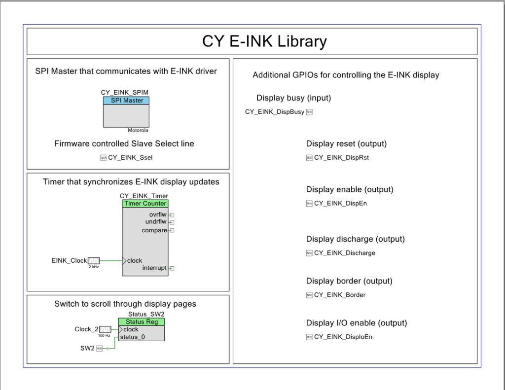
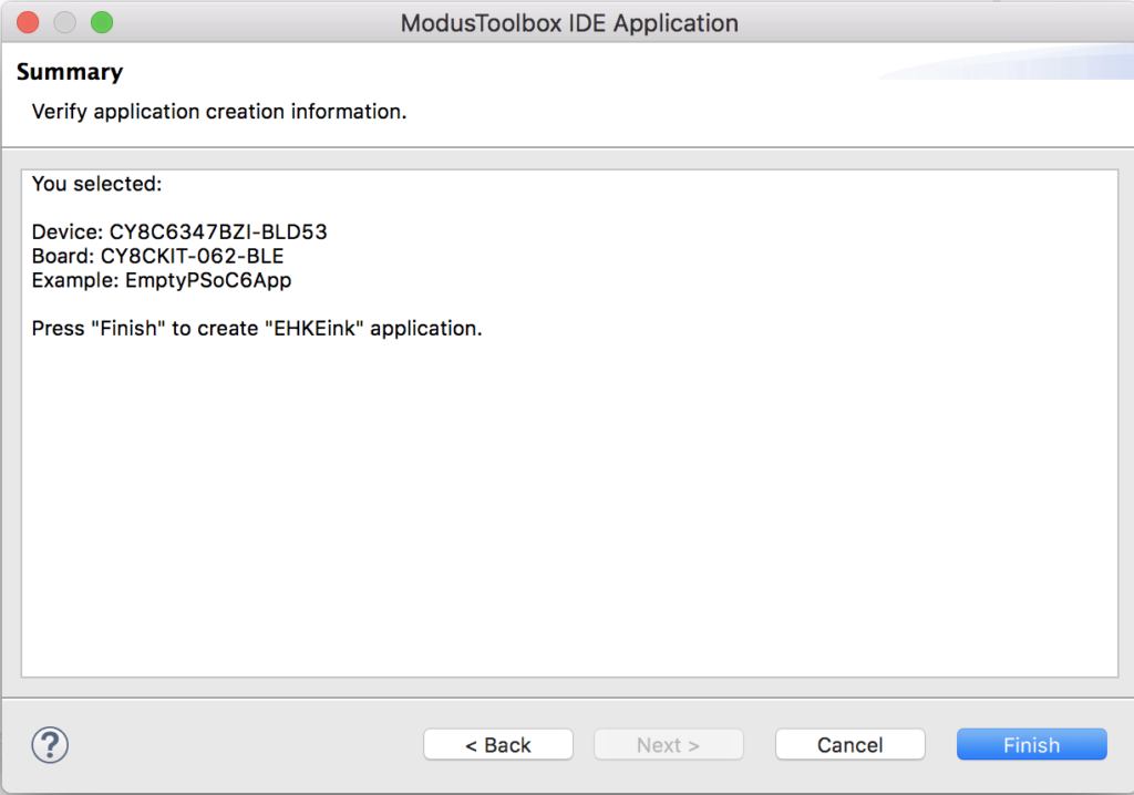
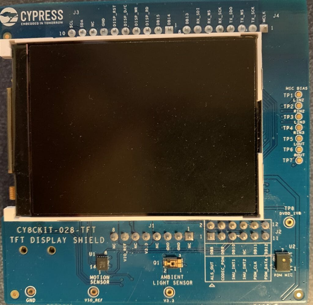
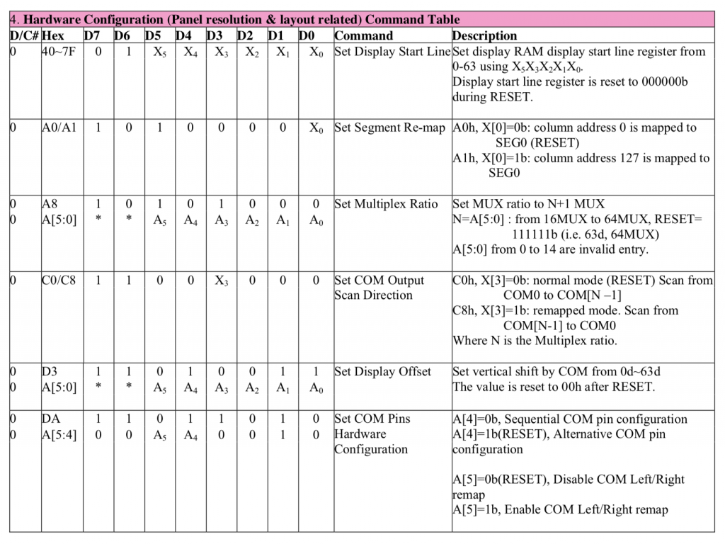
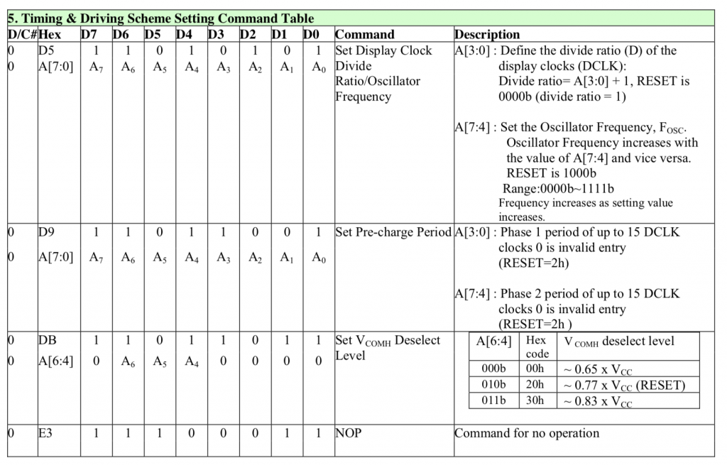
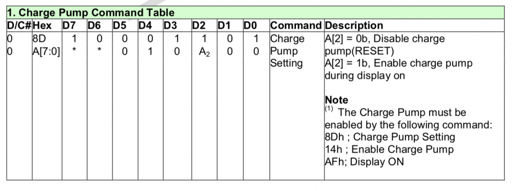
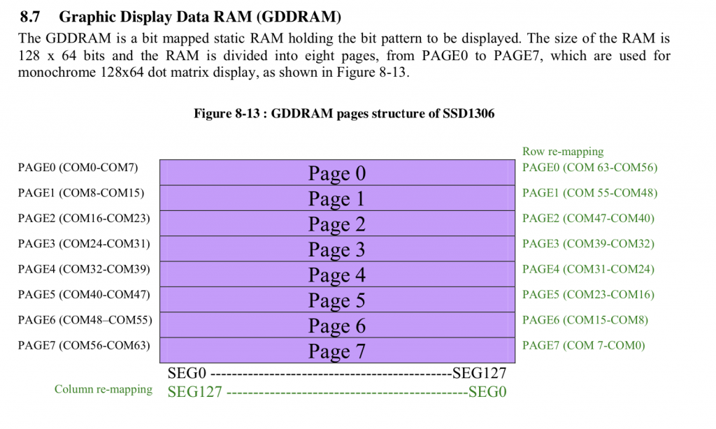
Summary
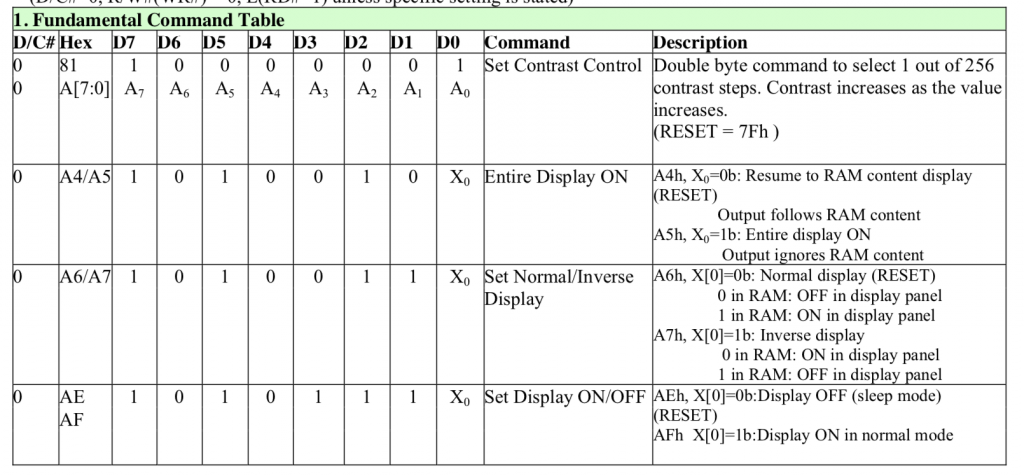
Have you ever wondered about the nature of time? Given the demographics of my readers I am quite sure that all of you have pondered this topic. In this article I will solve one of the great mysteries of human kind. What time is it? Well that may be a little bit over dramatic 🙂 Actually what I will show you is how to use the CY8CKIT-062S2-43012 development kit to get time from the internet using the Network Time Protocol (NTP), update the PSoC 6 RTC and display it on the CY8CKIT-028-TFT using MBED OS.
Unfortunately I will not show you a beautiful way to convert UTC to Eastern Time because I don’t actually know what that way would be which is very frustrating. Every way that I know requires me to drag a lot of crap into my PSoC6 which I don’t really want to do.
For this article I will discuss:
- MBED OS Project Setup
- MBED OS Event Queues
- The RTOS Architecture
- The Display Function(s)
- The NTP Thread
- The WiFI/Main Thread
- The Whole Program
Project Setup: Create and Configure Project + Add the Libraries
You should start this project by creating a project by running “mbed new NTPDemo” or by using mbed studio to create a new project. To run this project requires at least mbed-os-5.13.3. You have two basic choices to get the latest mbed. For some reason which I don’t totally understand when you run mbed new it gives you a slightly older version of mbed-os. To get a new version you can either “cd mbed-os ; mbed update mbed-os-5.13.3” or to get the latest “cd mbed-os ; mbed update master”.
In this project I use three libraries, emWin, the IoT Expert ST7789V library (for the display) and the ntp-client library. To add them run
- mbed add https://github.com/cypresssemiconductorco/emwin
- mbed add https://github.com/ARMmbed/ntp-client/
- mbed add https://github.com/iotexpert/mbed-os-emwin-st7789v
The emWin library requires that you tell emWin about which version of the library .a to link with. You can do this by adding this to the mbed_app.json
{
    "target_overrides": {
        "*": {
            "target.components_add": ["EMWIN_OSNTS"]
        }
    }
}
MBED OS Event Queues
For this project I will use one of the cool RTOS mechanisms that is built into MBED OS, the “EventQueue“. There is a nice tutorial in the MBED OS documentation. An EventQueue is a tool for running a function “later” and in a different thread context. What does that mean? It means that there is a thread that sits around waiting until you tell it to run a function. You tell it to run the function by pushing a function pointer into it’s EventQueue. In other words, an EventQueue is a thread that waits for functions to be pushed into queue. When the function is pushed into the queue it runs it.
How is this helpful? There are a several of reasons.
- If you are in an ISR it allows you to defer execution of something to the main program.
- It can be used to serialize access to some resource – in my case the display.
- It allows you to schedule some event to happen regularly
When MBED OS starts it automatically creates two of these event queues one of the queue threads runs at “osPriorityNormal” and can be accessed via mbed_event_queue(); The other event queue runs at “osPriorityHigh” and can be accesed by mbed_highprio_event_queue(); For some reason (which I don’t understand) these queues are documented on a separate page.
The RTOS Architecture
Here is a picture of the architecture of my program.

The Main Thread
The main function which is also the main thread, which then becomes the WiFi Thread
- Initializes the GUI
- Starts up the Display Event Queue
- Turns on the WiFi and attaches a callback (to notify the program of WiFI Status Changes)
- Try’s to connect to the WiFi Network
- If it fails, it updates the display and try’s again after 2 seconds
- Once it is connected it starts up the NTP Server Thread
- And then waits for the WiFi semaphore to be set… which only happens if WiFi gets disconnected at which point it goes back to the start of the WiFI connection and try again.
int main()
{
int wifiConnectionAttempts;
int ret;
GUI_Init();
displayQueue = mbed_event_queue();
displayQueue->call_every(1000, &updateDisplayTime);
wifi = WiFiInterface::get_default_instance();
wifi->attach(&wifiStatusCallback);
while(1)
{
wifiConnectionAttempts = 1;
do {
ret = wifi->connect(MBED_CONF_APP_WIFI_SSID, MBED_CONF_APP_WIFI_PASSWORD, NSAPI_SECURITY_WPA_WPA2);
displayQueue->call(updateDisplayWiFiConnectAttempts,wifiConnectionAttempts);
if (ret != 0) {
wifiConnectionAttempts += 1;
wait(2.0); // If for some reason it doesnt work wait 2s and try again
}
} while(ret !=0);
// If the NTPThread is not running... then start it up
if(netTimeThreadHandle.get_state() == Thread::Deleted)
netTimeThreadHandle.start(NTPTimeThread);
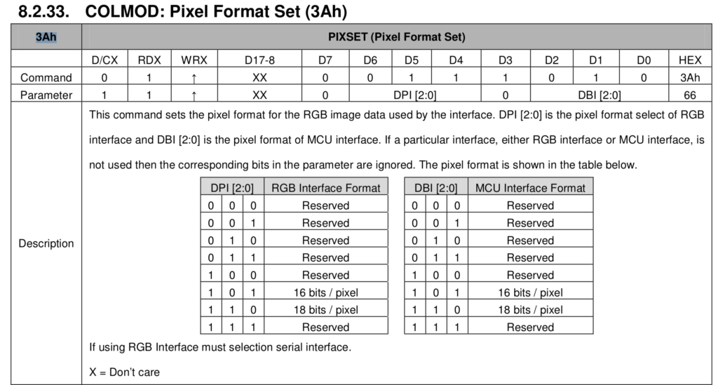
WiFiSemaphore.acquire();
}
Display Event Queue
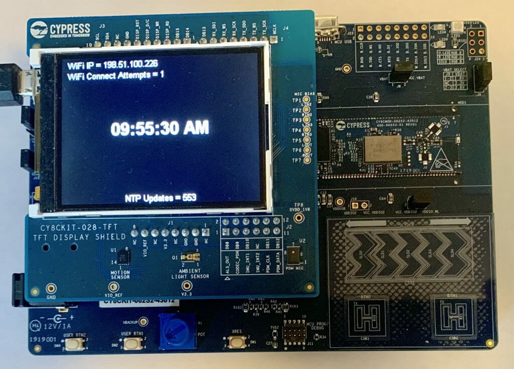
Display EventQueue is used to run functions which update the display. By using an EventQueue it ensure that the Display updates happen serially and there are no display resource conflicts. The four functions are
- updateDisplayWiFiStatus
- updateDisplayWifiConnectAttempts
- updateDisplayNTPCount
- updateDisplayTime
I wanted a function which could display the state of the WiFi connection on the screen. This is a string of text which is generated in the connection status function. In order to send the message, the connection status function will “malloc” which then requires the updateDisplayWiFiStatus function to free the memory associated with the message.
#define DISP_LEFTMARGIN 10
#define DISP_TOPMARGIN 4
#define DISP_LINESPACE 2
// updateDisplayWiFiStatus
// Used to display the wifi status
void updateDisplayWiFiStatus(char *status)
{
    GUI_SetFont(GUI_FONT_16_1);
    GUI_DispStringAt(status,DISP_LEFTMARGIN, DISP_TOPMARGIN);
    free(status);
}
When I started working on this program I had a bug in my connections so I added the ability to tell how many WiFI connections attempts had happened. I also wondered how many times there might be a disconnect if I ran this program a long time. The answer is I ran it for two days and it didn’t disconnect a single time. This function simply takes a number from the caller and displays it on the screen. Notice that I use snprintf to make sure that I don’t overrun the buffer (which I doubt could happen because I made it 128 bytes).
// updateDisplayWiFiConnectAttempts
// This function displays the number of attempted connections
void updateDisplayWiFiConnectAttempts(int count)
{
    char buffer[128];
    snprintf(buffer,sizeof(buffer),"WiFi Connect Attempts = %d",count);
    GUI_SetFont(GUI_FONT_16_1);
    GUI_DispStringAt(buffer,DISP_LEFTMARGIN, DISP_TOPMARGIN + (GUI_GetFontSizeY()+DISP_LINESPACE) );
}
I was curious how many times the NTP connection would happen. So I added the ability to display a count. Notice that I use a static variable to keep track of the number of times this function is called rather than pushing the number as an argument. Perhaps this is a design flaw?
// updateDisplayNTPCount
// updates the display with the number of time the NTP Server has been called
void updateDisplayNTPCount(void)
{
    static int count=0;
    char buffer[128];
    count = count + 1;
    snprintf(buffer,sizeof(buffer),"NTP Updates = %d\n",count);
    GUI_SetFont(GUI_FONT_16_1);
    GUI_DispStringHCenterAt(buffer,LCD_GetXSize()/2,LCD_GetYSize() - GUI_GetFontSizeY()); // near the bottom
}
The main display function is the seconds which is displayed in the middle of the screen. I get the time from the RTC in the PSoC and is set by the NTP Server. Notice my rather serious hack to handle the Eastern time difference to UTC… which unfortunately only works in the Summer.
// updateDisplayTime
// This function updates the time on the screen
void updateDisplayTime()
{
  time_t rawtime;
  struct tm * timeinfo;
  char buffer [128];

  time (&rawtime);
  rawtime = rawtime - (4*60*60); // UTC - 4hours ... serious hack which only works in summer

  timeinfo = localtime (&rawtime);
  strftime (buffer,sizeof(buffer),"%r",timeinfo);
  GUI_SetFont(GUI_FONT_32B_1);
  GUI_DispStringHCenterAt(buffer,LCD_GetXSize()/2,LCD_GetYSize()/2 - GUI_GetFontSizeY()/2);
}
NTP Time Thread
The Network Time Protocol was invented in 1981 by Dr. David Mills for use in getting Internet connected computers to have the right time. Since then it has been expanded a bunch of times to include Cellular, GPS and other networks. The scheme includes methods for dealing with propogation delay etc. However, for our purposes we will just ask one of the NIST computers, what time is it?
The way it works is that you setup a structure with 48 bytes in it. Then you open a UDP connection to an NTP server (which NIST runs for you) then it will fill out the same structure with some time data and send it back to you. Here is the packet:
typedef struct
{

  uint8_t li_vn_mode;      // Eight bits. li, vn, and mode.
                           // li.   Two bits.   Leap indicator.
                           // vn.   Three bits. Version number of the protocol.
                           // mode. Three bits. Client will pick mode 3 for client.

  uint8_t stratum;         // Eight bits. Stratum level of the local clock.
  uint8_t poll;            // Eight bits. Maximum interval between successive messages.
  uint8_t precision;       // Eight bits. Precision of the local clock.

  uint32_t rootDelay;      // 32 bits. Total round trip delay time.
  uint32_t rootDispersion; // 32 bits. Max error aloud from primary clock source.
  uint32_t refId;          // 32 bits. Reference clock identifier.

  uint32_t refTm_s;        // 32 bits. Reference time-stamp seconds.
  uint32_t refTm_f;        // 32 bits. Reference time-stamp fraction of a second.

  uint32_t origTm_s;       // 32 bits. Originate time-stamp seconds.
  uint32_t origTm_f;       // 32 bits. Originate time-stamp fraction of a second.

  uint32_t rxTm_s;         // 32 bits. Received time-stamp seconds.
  uint32_t rxTm_f;         // 32 bits. Received time-stamp fraction of a second.

  uint32_t txTm_s;         // 32 bits and the most important field the client cares about. Transmit time-stamp seconds.
  uint32_t txTm_f;         // 32 bits. Transmit time-stamp fraction of a second.

} __PACKED ntp_packet_t;              // Total: 384 bits or 48 bytes.
The code to send the packet is really simple. The only trick is that when you send data on the network you almost always use big endian, so you need to use the function nthol to convert.
void NTPClient::set_server(char* server, int port) {
    nist_server_address = server;
    nist_server_port = port;
}

time_t NTPClient::get_timestamp(int timeout) {
    const time_t TIME1970 = (time_t)2208988800UL;
    int ntp_send_values[12] = {0};
    int ntp_recv_values[12] = {0};

    SocketAddress nist;

    if (iface) {
        int ret_gethostbyname = iface->gethostbyname(nist_server_address, &nist);

        if (ret_gethostbyname < 0) {
            // Network error on DNS lookup
            return ret_gethostbyname;
        }

        nist.set_port(nist_server_port);

        memset(ntp_send_values, 0x00, sizeof(ntp_send_values));
        ntp_send_values[0] = '\x1b';

        memset(ntp_recv_values, 0x00, sizeof(ntp_recv_values));

        UDPSocket sock;
        sock.open(iface);
        sock.set_timeout(timeout);

        sock.sendto(nist, (void*)ntp_send_values, sizeof(ntp_send_values));

        SocketAddress source;
        const int n = sock.recvfrom(&source, (void*)ntp_recv_values, sizeof(ntp_recv_values));

        if (n > 10) {
            return ntohl(ntp_recv_values[10]) - TIME1970;
The times in the structure are represented with two 32-bit numbers
- # of seconds since 1/1/1900 (notice this is not 1970)
- # of fractional seconds in 1/2^32 chunks (that ain’t a whole lotta time)
The four numbers are
- Reference Time – when you last sent a packet
- Origin Time – when you sent the packet (from your clock)
- Receive Time – when the NTP server received your packet
- Transmit Time – when your NTP server sent the packet back to you
You know when you send the packet – called T1. You know when you received the packet – called T4. You know when the other side received your packet – called T2 and you know when the other side sent the packet called T3. With this information you can calculate the network delay, stability of the clocks etc. However, the simplest thing to do is to take the transit time, which is in UTC, and set your clock assuming 0 delay.
In MBEDOS to set the RTC clock in the PSoC you call the function with the number of seconds since 1/1/1970. Don’t forget that the time that comes back from NTP is in seconds since 1/1/1900.
set_time(timestamp);
Given that the PSoC 6 RTC counts in seconds you can just ignore the partial seconds.
WiFi Semaphore
At the top of main I registered to WiFi that I want a callback when the state of the WiFi changes.
wifi->attach(&wifiStatusCallback);
This function does two things.
- Updates the screen as the state goes from unconnected to connected
- Unlocks a semaphore to tell the main thread to reconnect.
// wifiStatusCallback
// Changes the display when the wifi status is changed
void wifiStatusCallback(nsapi_event_t status, intptr_t param)
{
    const int buffSize=40;
    char *statusText;
    statusText = (char *)malloc(buffSize);

    switch(param) {
        case NSAPI_STATUS_LOCAL_UP:
            snprintf(statusText,buffSize,"WiFi IP = %s",wifi->get_ip_address());
            break;
        case NSAPI_STATUS_GLOBAL_UP:
            snprintf(statusText,buffSize,"WiFi IP = %s",wifi->get_ip_address());
            break;
        case NSAPI_STATUS_DISCONNECTED:
            WiFiSemaphore.release();
            snprintf(statusText,buffSize,"WiFi Disconnected");
            break;
        case NSAPI_STATUS_CONNECTING:
            snprintf(statusText,buffSize,"WiFi Connecting");
            break;
        default:
            snprintf(statusText,buffSize,"Not Supported");
            break;
    }
    displayQueue->call(updateDisplayWiFiStatus,statusText);
}
The Whole Program
Here is the whole program.
#include "mbed.h"
#include "GUI.h"
#include "mbed_events.h"
#include "ntp-client/NTPClient.h"
Thread netTimeThreadHandle;
WiFiInterface *wifi;
EventQueue *displayQueue;
Semaphore WiFiSemaphore;
/******************************************************************************************
*
* Display Functions
*
********************************************************************************************/
#define DISP_LEFTMARGIN 10
#define DISP_TOPMARGIN 4
#define DISP_LINESPACE 2
// updateDisplayWiFiStatus
// Used to display the wifi status
void updateDisplayWiFiStatus(char *status)
{
GUI_SetFont(GUI_FONT_16_1);
GUI_DispStringAt(status,DISP_LEFTMARGIN, DISP_TOPMARGIN);
free(status);
}
// updateDisplayWiFiConnectAttempts
// This function displays the number of attempted connections
void updateDisplayWiFiConnectAttempts(int count)
{
char buffer[128];
snprintf(buffer,sizeof(buffer),"WiFi Connect Attempts = %d",count);
GUI_SetFont(GUI_FONT_16_1);
GUI_DispStringAt(buffer,DISP_LEFTMARGIN, DISP_TOPMARGIN + (GUI_GetFontSizeY()+DISP_LINESPACE) );
}
// updateDisplayNTPCount
// updates the display with the number of time the NTP Server has been called
void updateDisplayNTPCount(void)
{
static int count=0;
char buffer[128];
count = count + 1;
snprintf(buffer,sizeof(buffer),"NTP Updates = %d\n",count);
GUI_SetFont(GUI_FONT_16_1);
GUI_DispStringHCenterAt(buffer,LCD_GetXSize()/2,LCD_GetYSize() - GUI_GetFontSizeY()); // near the bottom
}
// updateDisplayTime
// This function updates the time on the screen
void updateDisplayTime()
{
time_t rawtime;
struct tm * timeinfo;
char buffer [128];
time (&rawtime);
rawtime = rawtime - (4*60*60); // UTC - 4hours ... serious hack which only works in summer
timeinfo = localtime (&rawtime);
strftime (buffer,sizeof(buffer),"%r",timeinfo);
GUI_SetFont(GUI_FONT_32B_1);
GUI_DispStringHCenterAt(buffer,LCD_GetXSize()/2,LCD_GetYSize()/2 - GUI_GetFontSizeY()/2);
}
/******************************************************************************************
* NTPTimeThread
* This thread calls the NTP Timeserver to get the UTC time
* It then updates the time in the RTC
* And it updates the display by adding an event to the display queue
********************************************************************************************/
void NTPTimeThread()
{
NTPClient ntpclient(wifi);
while(1)
{
if(wifi->get_connection_status() == NSAPI_STATUS_GLOBAL_UP)
{
time_t timestamp = ntpclient.get_timestamp();
if (timestamp < 0) {
// probably need to do something different here
}
else
{
set_time(timestamp);
displayQueue->call(updateDisplayNTPCount);
}
}
wait(60.0*5); // Goto the NTP server every 5 minutes
}
}
/******************************************************************************************
*
* Main & WiFi Thread
*
********************************************************************************************/
// wifiStatusCallback
// Changes the display when the wifi status is changed
void wifiStatusCallback(nsapi_event_t status, intptr_t param)
{
const int buffSize=40;
char *statusText;
statusText = (char *)malloc(buffSize);
switch(param) {
case NSAPI_STATUS_LOCAL_UP:
snprintf(statusText,buffSize,"WiFi IP = %s",wifi->get_ip_address());
break;
case NSAPI_STATUS_GLOBAL_UP:
snprintf(statusText,buffSize,"WiFi IP = %s",wifi->get_ip_address());
break;
case NSAPI_STATUS_DISCONNECTED:
WiFiSemaphore.release();
snprintf(statusText,buffSize,"WiFi Disconnected");
break;
case NSAPI_STATUS_CONNECTING:
snprintf(statusText,buffSize,"WiFi Connecting");
break;
default:
snprintf(statusText,buffSize,"Not Supported");
break;
}
displayQueue->call(updateDisplayWiFiStatus,statusText);
}
int main()
{
int wifiConnectionAttempts;
int ret;
GUI_Init();
displayQueue = mbed_event_queue();
displayQueue->call_every(1000, &updateDisplayTime);
wifi = WiFiInterface::get_default_instance();
wifi->attach(&wifiStatusCallback);
while(1)
{
wifiConnectionAttempts = 1;
do {
ret = wifi->connect(MBED_CONF_APP_WIFI_SSID, MBED_CONF_APP_WIFI_PASSWORD, NSAPI_SECURITY_WPA_WPA2);
displayQueue->call(updateDisplayWiFiConnectAttempts,wifiConnectionAttempts);
if (ret != 0) {
wifiConnectionAttempts += 1;
wait(2.0); // If for some reason it doesnt work wait 2s and try again
}
} while(ret !=0);
// If the NTPThread is not running... then start it up
if(netTimeThreadHandle.get_state() == Thread::Deleted)
netTimeThreadHandle.start(NTPTimeThread);
WiFiSemaphore.acquire();
}
}


 \
\